Note : Les descriptions sont présentées dans la langue officielle dans laquelle elles ont été soumises.
CA 02275616 1999-06-15
WO 98/2636 PCT/SE97/00882
Device and method relating to protection of an object
against over-currents comprising over-current reduction.
FILED OF THE INVENTION AND PRIOR ART
This invention is related to a device in an electric power
plant for protection of an object connected to an electric
power network or another equipment in the electric power
plant from fault-related over-currents, the device com
prising a switching device in a line between the object
and the network/equipment. In addition, the invention
includes a method for protecting the object from over
currents.
The electric object in question is preferably formed by an
apparatus having a magnetic circuit requiring protection
against fault-related over-currents, i.e. in practice
short-circuit currents. As an example, the object may be a
transformer or reactor. The present invention is intended
to be applied in connection with medium or high voltage.
According to IEC norm, medium voltage refers to 1-72,5 kV
whereas high voltage is >72,5 kV. Thus, transmission, sub-
transmission and distribution levels are included.
In prior power plants of this nature one has resorted to,
for protection of the object in question, a conventional
circuit-breaker (switching device) of such a design that
it provides galvanic separation on breaking. Since this
circuit breaker must be designed to be able to break very
CA 02275616 1999-06-15
WO 98/27636 PCT/SE97/00882
2
high currents and voltages, it will obtain a comparatively
bulky design with large inertia, which reflects itself in
a comparatively long break-time. It is pointed out that
the over-current primarily intended is the short-circuit
current occurring in connection with the protected object,
for instance as a consequence of faults in the electric
insulation system of the protected object. Such faults
means that the fault current (short-circuit current) of
the external network/equipment will tend to flow through
the arc created in the object. The result may be a very
large breakdown. It may be mentioned that for the Swedish
power network, the dimensioning short-circuit cur-
rent/fault-current is 63 kA. In reality, the short-circuit
current may amount to 40-50 kA.
A problem with said circuit-breaker is the long-break time
thereof. The dimensioning break-time (IEC-norm) for com-
pletely accomplished breaking is 150 milliseconds (ms). It
is associated to difficulties to reduce this break-time to
less than 50-130 ms depending upon the actual case. The
consequence thereof is that when there is a fault in the
protected object, a very high current will flow through
the same during the entire time required for actuating the
circuit-breaker to break. During this time the full fault
current of the external power network involves a consider-
able load on the protected object. In order to avoid dam-
age and complete breakdown with respect to the protected
object, one has, according to the prior art, constructed
the object so that it manages, without appreciable damage,
to be subjected to the short-circuit current/fault current
during the break-time of the circuit breaker. It is
pointed out that a short-circuit current (fault current)
in the protected object may be composed of the own contri-
bution of the object to the fault current and the current
addition emanating from the network/equipment. The own
contribution of the object to the fault current is not
CA 02275616 1999-06-15
WO 98/27636 PCT/SE97/00882
3
influenced by the functioning of the circuit-breaker but
the contribution to the fault current from the net-
work/equipment depends upon the operation of the circuit
breaker. The requirement for constructing the protected
object so that it may withstand a high short-circuit cur-
rent/fault current during a considerable time period means
substantial disadvantages in the form of more expensive
design and reduced performance.
Present day transformers and reactors rely, with respect
to protection, on their own inherent transient current
limiting ability, as a consequence of high inductance, in
addition to the function of the conventional circuit
breaker described above. Although the present invention is
applicable on such conventional transformeras and reac-
tors, it is with special advantage applicable on new in-
ventive transformers or reactors, which will be discussed
more in detail hereunder and which by their design present
a lower inductance/impedance than conventional transform-
ers and reactors and which therefore cannot constitute, to
an equally high degree, an inductively current limiting
unit involving an own protection against over-currents as
well as a protection for electric units located before and
after respectively the transformer/reactor. In such non
conventional transformers and reactors, it is of course
particularly important that the protection device operates
rapidly to delimit the damaging effect of the fault.
In order to simplify the understanding, a conventional
power transformer will be explained hereunder. What is
stated is in all essentials also applicable with respect
to reactors. Reactors may be designed as single-phase and
three-phase reactors. As regards insulation and cooling
there are, in principle, the same embodiments as for
transformers. Thus, air-insulated and oil-insulated, self-
cooled, pressure-oil-cooled, etc., reactors are available.
CA 02275616 1999-06-15
WO 98/27636 PCT/SE97/00882
4
Although reactors have one winding (per phase) and may be
designed both with and without an iron core, the following
description is to a large extent relevant also to reac-
tors.
A conventional power transformer comprises a transformer
core, in the following referred to as a core, often of
laminated oriented sheet, usually of silicone iron. The
core comprises a number of core limbs, connected by jokes
which together form one or more core windows. Transformers
with such a core are often referred to as core transform-
ers. Around the core limbs there are a number of windings
which are normally referred to as primary, secondary and
control windings. As far as power transformers are con-
cerned, these windings are practically always concentri-
cally arranged and distributed along the length of the
core limbs. The core transformer normally has circular
coils as well as a tapering core limb section in order to
fill up coils as closely as possible.
Sometimes also other types of core designs occur, for
example those which are included in so called shell-type
transformers. These have as a rule rectangular coils and a
rectangular limb section.
Conventional power transformers, in the lower part of the
power range in question, namely from 1 VA to the 1000 MVA
range, are sometimes designed with air-cooling to carry
away the unavoidable inherent losses. For protection
against contact, and possibly for reducing the external
magnetic field of the transformer, it is often provided
with an outer casing provided with ventilation openings.
Most of the conventional power transformers, however, are
oil-cooled. One of the reasons therefore is that the oil
has the additional very important function as insulating
CA 02275616 1999-06-15
WO 98/27636 PCT/SE97/00882
medium. An oil-cooled and oil-insulated conventional power
transformer must therefor be surrounded by en external
tank on which, as will be clear from the description be-
low, very high demands are placed.
5
Conventional oil-insulated power transformers are also
manufactured with water-cooling of the oil.
The following part of the description will for the most
part refer to conventional oil filled power transformers.
The windings mentioned above are formed from one or more
series-connected coils built up of a number of series-
connected turns. In addition, the coils are provied with a
special device to allow switching between the terminals of
the coils. Such a device may be designed for changeover
with the aid of screw joints or more often with the aid of
a special switch which is operable in the vicinty of the
tank. In the event that switching can take place for a
transformer under voltage, the changeover switch is re-
ferred to as an on-load tap changer whereas otherwise it
is referred to as a de-energized tap changer.
Regarding oil-cooled and oil-insulated power transformers
in the upper power range, the breaking element of the on-
load tap changers are placed in spceial oil-filled con-
tainers with direct connection to the transformer tank.
The breaking elements are operated purely mechanically via
a motor driven rotating shaft and are arranged so as to
obtain a fast movement during the switching when the con-
tact is open and a slower movement when the contact is to
be closed. The on-load tap changer as such, however, are
placed in the actual transformer tank. During the opera-
tion, arcing and sparking arise. This leads to degradation
of the oil in the containers. In order to obtain less arcs
and hence also less formation of soot and less wear on the
CA 02275616 1999-06-15
WO 98/27636 PCT/SE97/00882
6
contacts, the on-load tap changers are normally connected
to the high-voltage side of the transformer. This is due
to the fact that the currents which need to be broken and
connected, respectively, are smaller on the high-voltage
side than if the on-load tap changers were to be connected
to the low-voltage side. Failure statistics of conven-
tional oil-filled power transformers show that it is often
the on-load tap changers which give rise to faults.
In the lower power range of oil-cooled and oil-insulated
power transformers, both the on-load tap changers and
their breaking element are placed inside the tank. This
means that the above-mentioned problems with degradation
of the oil because of arcs during operation etc. effect
the whole oil system.
A considerable difference between a conventional power
transformer and such a non-conventional power transformer
intended with the invention refers to the conditions with
respect to insulation. For that reason it will be de-
scribed more in detail with reference to Fig 1 why the
insulation system is built as it is in conventional power
transformers.
From the point of view of applied or induced voltage, it
can broadly be said that a voltage which is stationary
across a winding is distributed equally onto each turn of
the winding, that is the turn voltage is equal on all
turns.
From the point of view of electric potential, however, the
situation is completely different. One end of a winding,
assuming the lower end of a winding 27 ccording to Fig 6,
is normally connected to earth. This means, however, that
the electric potential of each turn increases linearly
from practically zero in the turn which is nearest the
CA 02275616 1999-06-15
WO 98/27636 PCTISE97100882
7
earth potential up to a potential in the turns which are
at the other end of the winding which correspond to the
applied voltage.
In Fig 6, which in addition to a winding 27 comprises a
core 28, a simplified and fundamental view of the equipo-
tential lines 29 with respect to the electric field dis-
tribution is shown for a conventional winding for a case
where the lower part of the winding is assumed to be at
earth potential. This potential distribution determines
the composition of the insulation system, since it it
necessary to have sufficient insulation both between adja-
cent turns of the winding and between each turn and earth.
Thus, the Figure shows that the upper part of the winding
is subjected to the highest insulation loads. The design
and location of a winding relative to the core are in this
way determined substantially by electric field distribu-
tion in the core window.
The turns in an individual coil are normally brought to-
gether into a geometrical coherent unit, physically delim-
ited from the other coils. The distance between the coils
is also determined by the di-electric stress which may be
allowed to occur between the coils. Thus, this means that
a certain insulation distance is also required between the
coils. According to the above, sufficient insulation dis-
tances are also required to the other electrically con-
ducting objects which are within the electric field from
the electric potential occurring locally in the coils.
Thus, it is clear from the above description that for the
individual coils, the voltage difference internally be-
tween physically adjacent conductor elements is relatively
low whereas the voltage difference externally in relation
to other metal objects, including the other coils, may be
relatively high. The voltage difference is determined by
CA 02275616 1999-06-15
WO 98/27636 PCT/SE97/00882
8
the voltage induced by magnetic induction as well as by
the capacitively distributed voltages which may arise from
a connected external electrical system on the external
connections of the transformer. The voltage types which
may enter externally comprise, in addition to operating
voltage, lightening over-voltages and switching over-volt-
ages.
In the current leads of the coils, additional losses arise
as a result of the magnetic leakage field around the con-
ductor. To keep these losses as low as possible, espe-
cially for power transformers in the upper power range,
the conductors are normally divided into a number of con-
ductor element, often referred to as strands, which are
parallel-connected during operation. These strands must be
transposed according to such a pattern that the induced
voltage in each strand becomes as identical as possible
and so that the difference in induced voltage between each
pair of strands becomes as small as possible for inter-
nally circulating current components to be kept down at a
reasonable level from the loss point of view.
When designing transformers according to the prior art,
the general aim is to have as large a quantity of conduc-
for material as possible within a given area limited by
the so called transformer window, generally described as
having as high a fill factor as possible. The available
space shall comprise, in addition to the conductor mate-
rial, also the insulating material associated with the
coils, partly internally between the coils and partly to
other metallic components including the magnetic core.
The insulation system, partly within a coil/winding and
partly between coils/windings and other metal parts, is
normally designed as a solid cellulose- or varnish-based
insulation nearest the individual conductor element, and
CA 02275616 1999-06-15
WO 98/27636 PCT/SE97100882
9
outside of this as solid cellulose and liquid, possibly
also gaseous, insulation. Windings with insulation and
possible bracing parts in this way represent large vol-
umes which will be subjected to high electric field
strengths which arise in and around the active electro-
magnetic parts of the transformer. To be able to prede-
termine the dielectric stresses which arise and achieve
a good dimensioning with a minimum risk of breakdown,
good knowledge of the properties of insulating materials
is required. It is also important to achieve such a sur-
rounding environment that it does not change or reduce
the insulating properties.
The currently predominant insulation system for high-
voltage conventional power transformers comprises cellu-
lose material as the solid insulation and transformer
oil as the liquid insulation. The transformer oil is
based on so-called mineral oil.
Transformer oil has a dual function since, in addition
to the insulating function, it actively contributes to
cooling of the core, the winding, etc, by removal of the
loss heat of the transformer. Oil cooling requires oil
pump, an external cooling element, and expansion coupl
ing etc.
The electrical connection between the external connec-
tions of the transformer and the immediately connected
coils/windings is referred to as a bushing aiming at a
conductive connection through the tank which, in the
case of oil-filled power transformers, surround the ac-
tual transformer. The bushing is also a separate compo-
nent fixed to the tank and is designed to withstand the
insulation requirements being made, both on the outside
and the inside of the tank, while at the same time it
CA 02275616 1999-06-15
WO 98/27636 PCT/SE97/00882
should withstand the current loads occurring and the en-
suing current forces.
It should be pointed out that the same requirements for
5 the insulation system as described above regarding the
windings also apply to the necessary internal connec-
tions between the coils, between bushings and coils,
different types of change-over switches and the bushings
as such.
All the metallic components inside a conventional power
transformer are normally connected to a given ground po-
tential with the exception of the current-carrying con-
ductors. In this way, the risk of an unwanted, and dif-
ficult-to-control, potential increase as a result of ca-
pacity voltage distribution between current leads at
high potential and ground is avoided. Such an unwanted
potential increase may give rise to partial discharges,
so-called corona. Corona may be revealed during the nor-
mal acceptance tests, which partially are performed,
compared with rated data, increased voltage and fre-
quency. Corona may give rise to damage during operation.
The individual coils in a transformer must have such a
mechanical dimensioning that they may withstand any
stresses occurring as a consequence of currents arising
and the resultant current forces during a short-circuit
process. Normally, the coils are designed such that the
forces arising are absorbed within each individual coil,
which in turn may mean that the coil can not be
dimensioned optimally for its normal function during
normal operation.
CA 02275616 1999-06-15
WO 98/27636 PCT/SE97/00882
11
Within a narrow voltage and power range of oil-filled
power transformers, the windings are designed as so-
called sheet windings. This means that the individual
conductors mentioned above are replaced by thin sheets.
Sheet-wound power transformers are manufactured for
voltages of up to 20-30 kV and powers of up to 20-30 MW.
The insulation system of conventional power transformers
within the upper power range requires, in addition to a
relatively complicated design, also special manufactur-
ing measures to utilize the properties of the insulation
system in the best way. For a good insulation to be ob-
tained, the insulation system shall have a low moisture
content, the solid part of the insulation shall be well
impregnated with the surrounding oil and the risk of re-
maining "gas" pockets in the solid part must be minimal.
To ensure this, a special drying and impregnating proc-
ess is carried out on a complete core with windings be-
fore it is lowered into a tank. After this drying and
impregnating process, the transformer is lowered into
the tank which is then sealed. Before filling of oil,
the tank with the immersed transformer must be emptied
of all air. This is done in connection with a special
vacuum treatment. When this has been carried out, fill
ing of oil takes place.
To be able to obtain the promised service life, etc, of
a conventional oil-filled transformer, pumping out to
almost absolute vacuum is required in connection with
the vacuum treatment. Thus, this presupposes that the
tank which surrounds the transformer is designed for
full vacuum, which entails a considerable consumption of
material and manufacturing time.
If electric discharges occur in an oil-filled power
transformer, or if a local considerable increase of the
CA 02275616 1999-06-15
WO 98/27636 PCT/SE97/00882
12
temperature in any part of the transformer occurs, the
oil is disintegrated and gaseous products are dissolved
in the oil. The transformers are therefore normally pro
vided with monitoring devices for detecting of gas dis
solved in the oil.
For weight reasons, large power transformers are trans-
ported without oil. In situ installation of the trans-
former at a customer requires, in turn, renewed vacuum
treatment. In addition, this is a process which has to
be repeated each time the tank is opened for some action
or inspection.
It is obvious that these processes are very time-consum-
ing and cost-demanding and constitute a considerable
part of the total for manufacturing and repair while at
the same time requiring access to extensive resources.
The insulating material in a conventional power trans-
former consitutes a large part of the total volume of the
transformer. For a conventional power transformer the
upper power range, oil quantities in the order of magni-
tude of several tens of cubic meters of transformer oil
are not unusual. The oil which exhibits a certain similar-
ity to diesel oil is thinly fluid and exhibits a rela
tively low flash point. Thus, is is obvious that oil to
gether with the cellulose constitutes a non-negligeable
fire hazard in the case of unintentional heating, for
example at an internal flashover, and a resultant oil
spillage.
It is also obvious that, especially in conventional oil-
filled power transformers, there is a very large transport
problem. A conventional oil-filled power transformer in
the upper power range may have a total oil volume of 40-50
cubic meters and may have a weight of up to 30-40 tons.
CA 02275616 1999-06-15
WO 98/27636 PCT/SE97/00882
13
For conventional power transformers in the upper power
range, transport often occurs with a tank without oil. It
happens that the external design of the transformer must
be adapted to the current transport profile, that is for
any passage of bridges, tunnels etc..
Here follows a short summary of what can be described as
limitation and problem areas according to prior art with
respect to oil-filled power transformers:
An oil-filled conventional power transformer
- comprises an outer tank which is to house a transformer
comprising a transformer core with coils, oil for insula-
tion and cooling, mechanical bracing devices of various
kinds etc. Very large mechanical demands are placed on the
tank, since, without oil but with a transformer, it shall
be capable of being vacuum-treated to practically full
vacuum. The need for an external tank require very exten-
sive manufacturing and testing processes. Furthermore, the
tank means that external measures of the transformer be-
come much larger than for a so called "dry" transformer
for the same power. The larger external measures also
normally entail considerable transport problems.
- normally comprises a so called pressure-oil-cooling.
This cooling method requires access to an oil pump, an
external cooling element, an expansion vessel and an ex-
pansion coupling etc.
- comprises an electrical connection between the external
connections of the transformer and the immediately con-
nected coils/windings in the form of a bushing fixed to
the tank. The bushing is designed to withstand any insula-
tion requirements made, both regarding the outside and the
inside of the tank.
CA 02275616 1999-06-15
WO 98/27636 PCT/SE97/00882
14
- comprises coils/windings whose conductors are divided
into a number of conductor elements, strands, which have
to be transposed in such a way that the voltage induced in
each strand becomes as identical as possible and such that
the difference in induced voltage between each pair of
strands becomes as small as possible.
- comprises an insulation system, partly within a
coil/winding and partly between coils/windings and other
metal parts, which system is designed as a solid cellulose
or warnish-based insulation nearest the individual conduc-
tor element and, outside of this, solid cellulose and a
liquid, possibly also gaseous, insulation. In addition, it
is extremely important that the insulation system exhibits
a very low moisture content.
- comprises as an integrated part an on-load tap changer,
surrounded by oil and normally connected to the high volt-
age winding of the transformer for voltage control.
- involves a non-negligeable fire hazard in connection
with internal partial discharges, so called corona, spark-
ing in on-load tap changers and other fault conditions.
- comprises normally a monitoring device for monitoring
gas dissolved in the oil, which occurs in case of electri-
cal discharges therein and in case of local increases of
the temperature.
- may result, in the event of damage or accident, in oil
spillage leading to extensive environmental damage.
CA 02275616 1999-06-15
WO 98/27636 PCT/SE97/00882
OBJECT OF THE INVENTION
The primary object of the present invention is to devise
ways to design the device and the method so as to achieve
5 better protection for the object and, accordingly, a re-
duced load on the same, a fact which means that the object
itself does not have to be designed to withstand a maximum
of short-circuit currents/fault currents during relatively
long time periods.
A secondary object with the invention is to design the
protection device and method such that an adequate protec-
tion is achieved for electric objects in the form of
transformers and reactors, the design of which is based
upon non-conventional design principles, which may mean
that the design does not have the same resistance to
fault-related over-currents, internal as well as external,
as the conventional present day conventional transformers
and reactors. However, the invention is of course also
intended to be applicable in connection with conventional
transformers and reactors.
SUMMARY OF THE INVENTION
According to the invention, the object indicated above is
achieved in that the line between the object and the
switching device is connected to an over-current reducing
arrangement, which is actuatable for over-current reduc-
tion with assistance of an over-current conditions detect-
ing arrangement within a time-period substantially less
than the break-time of the switching device.
Thus, the invention is based upon the principle not to
rely for breaking purposes only upon a switching device
which finally establishes galvanic separation, but instead
use a rapidly operating over-current reducing arrangement,
CA 02275616 1999-06-15
WO 98/27636 PCT/SE97/00882
16
which, without effecting any real breaking of the over-
current, nevertheless reduces the same to such an extent
that the object under protection will be subjected to
substantially reduced strains and, accordingly, a smaller
amount of damages. The reduced over-current/fault current
means, accordingly, that when the switching device estab-
lishes galvanic separation, the total energy injection
into the protected object will have been much smaller than
in absence of the over-current reducing arrangement.
According to a preferred embodiment of the invention, the
over-current reducing arrangement is designed as compris-
ing an over-current diverter for diversion of over-cur-
rents to earth or otherwise another unit having a lower
potential than the network/equipment.
According to a particularly preferred embodiment of the
invention, measures have been taken to obtain a reduction
of the time-period, during which the current already re-
duced by means of the over-current reducing arrangement
may flow into the protected object. For this purpose the
device comprises a further breaker arranged in the line
between the circuit breaker and the object, said further
breaker being designed to break at a lower voltage and
current than the switching device and therefore may be
designed with a shorter break-time than the switching
device as a consequence of a smaller need for movement and
a smaller weight of the movable contacts) of the breaker,
said further breaker being arranged to break not until a
time when the over-current towards or away from the pro-
tected object has been reduced by means of the over-cur-
rent reducing arrangement. More specifically, the movement
required of the movable contacts) of the further breaker
is smaller due to lower voltage whereas the weight of the
contacts) may be held lower due to the fact that the
lower current does not require such large contact areas.
CA 02275616 1999-06-15
WO 98/27636 PCT/SE97/00882
17
As is more closely defined in the claims, the invention
is applicable on transformers and reactors constructed
by means of unconventional technique, namely cable tech-
nology. These may under certain conditions become sensi-
tive to electric faults. Such a design may for instance
be given a lower impedance than what is considered con-
ventional today within the power field. This means that
the design does not have the same resistance against
fault-related overcurrents, internal as well as exter-
nal, as the conventional apparatus of today. If the ap-
paratus, besides, has been designed from the start to
operate with a higher electrical voltage than the con-
ventional apparatus of today, the strain on the electri-
cal insulation system of the apparatus, caused by the
resulting higher electrical field, becomes, of course,
greater. This means that the apparatus may be more effi-
cient, more economical, mechanically lighter, more reli-
able, less expensive to produce and generally more eco-
nomical than conventional apparatus and may manage with-
out the usual connection to other electromagnetic appa-
ratus, such an apparatus requires an adequate electric
protection to eliminate, or at least reduce, the conse-
quences of a breakdown in the apparatus in question. A
combination of the protection device according to the
invention and an apparatus designed in this way, prefer-
ably a transformer or reactor, means an optimization of
the plant in its entirety.
The non-conventional transformer intended here is a
power transformer with a rated power of from a few hund-
red kVA up to over 1000 MVA with a rated voltage of from
3-4 kV up to very high transmission voltages, such as
400 kV to 800 kV or higher, and which does not entail
the disadvantages, problems and limitations which are
associated with the prior art oil-filled power trans-
former according to what appears above.
CA 02275616 1999-06-15
WO 98/27636 PCT/SE97/00882
18
The invention is based on the realization that by design-
ing at least one winding in the trasformer/reactor such
that it comprises a solid insulation surrounded by an
outer and and an inner potential-equalizing semiconducting
layer, within which inner layer the at least one electric
conductor is disposed, a possibility is provided of main-
taining the electric field in the whole plant within the
conductor. The electric conductor is, according to the
invention, suitably so arranged that it has such conduct-
ing contact with the inner semiconducting layer that no
harmful potential differences may arise in the boundary
layer between the innermost part of the solid insulation
and the semiconducting layer located inwardly thereof.
Such a power transformer exhibits great advantages rela-
tive to a conventional oil-filled transformer. As men-
tioned by way of introduction, the invention also provides
for the concept to be applied to reactors both with and
without a core of magnetic material.
The essential difference between conventional oil-filled
power transformers/reactors and a power trans-
former/reactor according to the invention is that the
winding/windings thus comprise a solid insulation sur-
rounded by external and internal potential layers as well
as at least one electric conductor arranged inwardly of
the inner potential layer, said potential layers being
made from a semiconducting material. The definition of
what is comprised by the concept semiconductor will be
described below. According to a preferred embodiment, the
winding/windings is/are designed in the form of a flexible
cable.
At the high voltage levels which are required in a power
transformer/reactor according to the invention, which is
connected to high-voltage networks with very high operat-
CA 02275616 1999-06-15
WO 98/Z7636 PCT/SE97/00882
19
ing voltages, the electric and thermal loads which may
arise will impose extreme demands on the insulating mate-
rial. It is known that so called partial discharges, pd,
generally constitute a serious problem for the insulating
material in high-voltage installations. If cavities, pores
or the like arise at an insulating layer, internal corona
discharges may arise at high electric voltages, whereby
the insulating material is gradually degraded, which fi-
nally may lead to electric break-down through the insula-
tion. It is realized that this can lead to serious break-
down of, for example, a power transformer.
The invention is, inter alia, based on the realization
that it is of extreme importance that the semiconducting
potential layers exhibit similar thermal properties and
that the layers are firmly connected to the solid insula-
tion. The thermal properties in view here relate to coef-
ficient of thermal expansion. The inner and outer semicon-
ducting layers and the intermediate insulation should,
accordingly, be well integrated, i.e. in good contact with
each other over substantially the entire boundary layer,
independently of the temperature changes occurring at
different loads. Thus, the insulation including the sur-
rounding semiconducting layers will, at temperature gradi-
ents, constitute a monolithic part and defects caused by
different temperature expansion in the insulation and the
surrounding layers do not arise. The electric load on the
material is reduced as a consequence of the fact that the
semiconducting layers around the insulation will consti-
tute equipotential surfaces and that the electric field in
the insulation will hence be distributed uniformly over
the insulation.
According to the invention, it must be ensured that the
insulation is not broken down by the phenomena described
above. This can be achieved by using as insulation system
CA 02275616 1999-06-15
WO 98/27636 PCT/SE97I00882
semiconducting layers and intermediate insulation layer
produced in such a way that the risk for cavities and
pores is minimal, for example extruded layers of a suit-
able plastic material, such as XLPE (cross linked polyeth-
5 ylene) and EP-rubber (EP - ethylene-propylene). The insu-
lating material is thus a low-loss material with high
break-down strength.
It is known that transmission cables for high voltage
10 are designed with conductors having an extruded insula-
tion with an inner and outer semiconducting layer. In
transmission of electrical energy, one has since long
ago aimed at avoiding defects in the insulation. How-
ever, in high voltage transmission cables the electric
15 potential along the length of the cable is not changed,
but the potential lies, in principle, at the same level,
which means a high electric stress on the insulating ma
terial. The transmission cable is provided with one in
ner and one outer semiconducting layer for potential
20 equalization.
Thus, the winding is according to the invention provided
with a solid insulation and surrounding potential equal-
izing layers, whereby the transformer/reactor may be ob-
tained, in which the electrical field is retained within
the winding. Additional improvements may also be
achieved by constructing the conductor from smaller in-
sulated parts, so-called strands. By making these
strands small and circular, the magnetic field across
the strands will exhibit constant geometry in relation
to the field and the occurrence of eddy currents is
minimized.
According to the invention the winding/windings is/are
thus preferably made in the form of a cable comprising
at least one conductor comprising a number of strands
CA 02275616 1999-06-15
WO 98/27636 PCT/SE97/00882
21
and an inner semiconducting layer around the strands.
Outside of this inner semiconducting layer is the main
insulation of the cable in the form of a solid extruded
insulation, and around this insulation there is an outer
semiconducting layer. The cable may in certain connec-
tions have additional outer and inner layers. For in-
stance, further potential equalizing, semiconducting
layers could be arranged in the solid insulation between
those two layers which in this specification are denomi-
nated "inner" and "outer" In such a case, this addi-
tional layer will lie on a medium potential.
According to the invention, the outer semiconducting
layer shall exhibit such electrical properties that a
potential equalization along the conductor is ensured.
The semiconducting layer may, however, not exhibit such
conductivity properties that a current will be induced
in the layer, said current causing an unwanted thermal
load. However, the conducting properties of the layer
must be sufficient to ensure that the outer layer is ca-
pable of forming an equipotential surface. The inner
semiconducting layer must present a sufficient electri-
cal conductivity to be able to operate potential-equal-
izing and, accordingly, equalizing with regard to the
electrical field outside the inner layer. In this con-
nection it is important that the layer has such proper-
ties that it equalizes irregularities in the surface of
the conductor and so that the layer is capable of form-
ing an equipotential surface with a high surface finish
at the border layer to the rigid insulation. The inner
layer may be formed with a varying thickness but in or-
der to ensure an even surface with respect to the con-
ductor and the solid insulation, the thickness of the
layer should be between 0,5 and 1 mm. However, the inner
layer may not exhibit such a high electrical conduction
CA 02275616 1999-06-15
WO 98/27636 PCT/SE97/00882
22
capacity that the layer contributes to induction of
voltages.
The resistivity for the inner and outer layers should
lie in the range 10-6 S2cm - 100 kS2cm, suitably 10-3 -
1000 S2cm, preferably 1-500 S2,cm. Furthermore, it is pre-
ferred that the inner and outer layers each exhibit a
resistance, which per meter cable is in the range 50 x.52
- 5 MS2.
Thus, such a XLPE cable or a cable with EP rubber insu-
lation or a corresponding cable is used according to the
invention in a modified embodiment and in an entirely
new field of use as winding in a magnetic circuit.
A winding comprising such a cable will entail quite dif-
ferent conditions from the insulation point of view from
those which apply to conventional transformers/reactor
windings due to the electric field distribution. To
utilize the advantages afforded by the use of the men-
tioned cable, there are other possible embodiment as re-
gards grounding of a transformer/reactor according to
the invention than that which is applicable for conven-
tional oil-filled power transformers. These methods are
the subject matter of separate application for patent.
It is essential and necessary for a winding in a power
transformer/reactor according to the invention that at
least one of the strands of the conductor is uninsulated
and arranged such that good electrical contact is
achieved with the inner semiconducting layer. Thus, the
inner layer will always lie on the potential of the
conductor.
CA 02275616 1999-06-15
WO 98/27636 PCT/SE97/00882
23
As far the rest of the strands are concerned, all of
them or some of them may be insulated, for example by
being varnished.
Manufacturing transformer or reactor windings of a cable
according to the above entails drastic differences as
regards the electrical field distribution between con-
ventional power transformers/reactors and a power trans-
former/reactor according to the invention. The decisive
advantage with a cable-formed winding according to the
invention is that the electric field is enclosed in the
winding and that there is, thus, no electric field out-
side the outer semiconducting layer. The electric field
achieved by the current-carrying conductor occurs in es-
sential only in the solid main insulation. Hoth from the
design point of view and the manufacturing point of view
this means considerable advantages;
- The windings of the transformer may be formed without
having to consider any electric field distribution and
the transposition of strands, mentioned under the back-
ground art is omitted.
- The core design of the transformer may be formed with-
out having to consider any electric field distribution.
- No oil is needed for electrical insulation of the
winding, that is, the medium surround the winding may be
air.
- No special connections are required for electrical
connection between the outer connections of the trans-
former and the immediately connected coils/windings
since the electrical connection, contrary to conven-
tional plants, is integrated with the winding.
CA 02275616 1999-06-15
WO 98/27636 PCT/SE97/00882
24
- The manufacturing and testing technology which is
needed for a power transformer according to the inven-
tion is considerably simplier than for a conventional
power transformer/reactor since the impregnation, drying
and vacuum treatments described under the description of
the background art are not needed.
Further advantages and features of the invention, in
particular with respect to the method according to the
invention, appear from the following description and the
claims.
BRIEF DESCRIPTION OF THE DRAWINGS
With reference to the enclosed drawings, a more specific
description of an embodiment example of the invention
follows hereinafter.
In the drawings:
Fig 1 is a purely diagrammatical view illustrating the
basic aspects behind the solution according to
the invention,
Figs 2-
2d are diagrams illustrating in a diagrammatical
form and in a comparative way fault current de
velopments and the energy development with and
without the protection device according to the
invention;
Fig 3 is a diagrammatical view illustrating a conceiv-
able design of a device according to the inven-
tion;
CA 02275616 1999-06-15
WO 98/27636 PCT/SE97/00882
Fig 4 is a diagrammatical view illustrating a possible
design of the over-current reducing arrangement;
Fig 5 is a diagrammatical view illustrating the device
5 according to the invention applied in an elec-
trical power plant comprising a generator, a
transformer and a power network connected
thereto;
Fig 6 shows the electric field distribution about a
10 winding of a conventional power trans
former/reactor;
Fig 7 shows an example of~a cable used in the windings
of the power transformers/reactors according to
15 the invention, and
Fig 8 illustrates an embodiment of a power trans-
former according to the invention.
20 DETAILED DESCRIPTION OF PREFERRED EMBODIMENTS
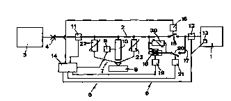
An electric power plant comprising a protected object 1 is
shown in Fig 1. As is described hereunder, this object
could for instance consist of a transformer or reactor.
25 This object is connected, via a line 2, to an external
distribution network 3. Instead of such a network, the
unit denoted 3 could be formed by some other equipment
contained in the power plant. The power plant involved is
conceived to be of such a nature that it is the object 1
itself which primarily is intended to be protected against
fault currents from the network/equipment 3 when there
occurs a fault in the object 1 giving rise to a fault
current from the network/equipment 3 towards the object 1
so that the fault current will flow through the object.
Said fault may consist in a short-circuit having been
formed a.n the object 1. A short-circuit is a conduction
CA 02275616 1999-06-15
WO 98/27636 PCT/SE97/00882
26
path, which is not intended, between two or more points.
The short-circuit may for instance consist of an arc. This
short-circuit and the resulting violent current flow may
involve considerable damage and even a total break-down of
the object 1.
It is already pointed out that with at least some types of
protected electrical objects 1, short-circuit cur-
rents/fault currents harmful to the object in question may
flow from the protected object towards the net-
work/equipment 3. Within the scope of the invention, it is
intended to be used for protection purposes not only for
protection of the object from externally emanating fault
currents flowing towards the object but also from internal
fault currents in the object flowing in the opposite di-
rection. This will be discussed in more detail in the
following.
In the following, the designation 3 will, to simplify the
description, always be mentioned as consisting of an ex-
ternal power network. However, it should be kept in mind
that some other equipment may be involved instead of such
a network, as long as said equipment causes violent cur-
rent flow through the object 1 when there is a fault.
A conventional circuit breaker 4 is arranged in the line 2
between the object 1 and the network 3. This circuit
breaker comprises at least one own sensor for sensing
circumstances indicative of the fact that there is an
overcurrent flowing in the line 2. Such circumstances may
be currents/voltages but also other indicating that a
fault is at hand. For instance, the sensor may be an arc
sensor or a sensor recording short circuit sound etc. When
the sensor indicates that the overcurrent is above a cer-
taro level, the circuit breaker 4 is activated for break-
ing of the connection between the object 1 and the network
CA 02275616 1999-06-15
WO 98/27636 PCT/SE97/00882
27
3. The circuit breaker 4 must, however, break the total
short circuit current/fault current. Thus, the circuit
breaker must be designed to fulfil highly placed require-
ments, which in practice means that it will operate rela-
y tively slowly. In Fig 2a it is illustrated in a cur-
rent/time-diagram that when a fault, for instance a short
circuit in the object 1, occurs at the time tfault~ the
fault current in the line denoted 2 in Fig 1 rapidly as-
sumes the magnitude i1. This fault current i1 is broken by
means of the circuit breaker 4 at t1, which is at least
within 150 ms after tfault~ Fig 2d illustrates the diagram
i2~t and, accordingly, the energy developed in the pro-
tected object 1 as a consequence of the short circuit
therein. The energy injection into the object occurring as
a consequence of the short-circuit current is, accord-
ingly, represented by the total area of the outer rectan-
gle in Fig 2d.
It is in this connection pointed out that the fault cur-
rent in Figs 2a-c and the currents in Fig 2d represent the
envelope of the extreme value. Only one polarity has been
drawn out in the diagram for the sake of simplicity.
The circuit breaker 4 is of such a design that it estab-
fishes galvanic separation by separation of metallic con-
tacts. Accordingly, the circuit breaker 4 comprises, as a
rule, required auxiliary equipment for arc extinguishing.
According to the invention the line 2 between the object 1
and the switching device 4 is connected to an arrangement
reducing overcurrents towards the apparatus 1 and gener-
ally denoted 5. The arrangement is actuatable for overcur-
rent reduction with the assistance of an overcurrent con-
ditions detecting arrangement within a time period sub-
stantially less than the break time of the circuit breaker
4. This arrangement 5 is, accordingly, designed such that
CA 02275616 1999-06-15
WO 98/27636 PCT/SE97/00882
28
it does not have to establish any galvanic separation.
Therefore, conditions are created to very rapidly estab-
lish a current reduction without having to accomplish any
total elimination of the current flowing from the network
3 towards the protected object 1. Fig 2b illustrates in
contrast to the case according to Fig 2a that the overcur-
rent reducing arrangement 5 according to the invention is
activated upon occurrence of a short circuit current at
the time tfault for overcurrent reduction to the level i2
at the time t2. The time interval tfault-t2 represents,
accordingly, the reaction time of the overcurrent reducing
arrangement 5. Hy the task of the arrangement 5 not to
break but only reduce the fault current, the arrangement
may be caused to react extremely rapidly, which will be
discussed more closely hereunder. As an example, it may be
mentioned that current reduction from the level i1 to the
level i2 is intended to be accomplished within one or a
few ms after unacceptable overcurrent conditions having
been detected. It is then aimed at to accomplish the cur-
rent reduction in a shorter time than 1 ms, and preferably
more rapidly than 1 microsecond.
As appears from Fig 1, the device comprises a further
breaker generally denoted 6 and arranged in the line 2
between the circuit breaker 4 and the object 1. This fur-
ther breaker is designed to break a lower voltage and
currents than the circuit breaker 4 and may, as a conse-
quence thereof, be designed to operate with shorter break
times than the circuit breaker. The further breaker 6 is
arranged to break not until after the overcurrent from the
network 3 towards the object 1 has been reduced by means
of the overcurrent reducing arrangement 5 but sub-
stantially earlier than the circuit breaker 4. From that
stated, it appears that the further breaker 6 should be
coupled to the line 2 in such a way that it is the current
reduced by means of the overcurrent reducing arrangement 5
CA 02275616 1999-06-15
WO 98/27636 PCT/SE97/00882
29
which will flow through the further breaker and which,
accordingly, is to be broken by means thereof.
Fig 2b illustrates the action of the further breaker 6.
This breaker is, more specifically, designed to break at
the time t3, which means that the duration of the current
i2 reduced by means of the overcurrent reducing
arrangement 5 is substantially delimited, namely to the
time period t2-t3. The consequence is that the energy
injection into the protected object 1 caused by a fault
current from the network 3 is represented by the surfaces
marked with oblique lines in Fig 2d. It appears that a
drastic reduction of the energy injection is achieved. In
this connection it is pointed out that since, according to
a specific model, the energy increases with the square of
the current, a reduction to one half of the current
reduces the energy injection to a fourth. It is
illustrated in Fig 2c how the fault current will flow
through the arrangement 5.
The dimensioning of the arrangement 5 and the further
breaker 6 is conceived to be carried out such that the
arrangement 5 reduces the fault current and the voltage to
be broken by means of the further breaker 6 to substan-
tially lower levels. A realistic break time as to the
further breaker 6 is 1 ms. However, the dimensioning
should be made such that the breaker 6 is caused to break
not until after the arrangement 5 having reduced the cur
rent flowing through the breaker 6 to at least a substan
tial degree.
It is illustrated in more detail in Fig 3 how the device
may be realised. It is then pointed out that the invention
is applicable in direct current (also HVDC = High Voltage
Direct Current) and alternating-current connections. In
the latter case, the line denoted 2 may be considered to
CA 02275616 1999-06-15
WO 98/27636 PCT/SE97/00882
form one of the phases in a multiphase alternating-current
system. However, it should be kept in mind that the device
according to the invention may be realised so that either
all phases are subjected to the protection function ac-
s cording to the invention in case of a detected fault or
that only that phase or those phases where a fault current
occurs which are subjected to current reduction.
It appears from Fig 3 that the overcurrent reducing ar-
10 rangement generally denoted 5 comprises an overcurrent
diverter 7 for diverting overcurrents to earth 8 or other-
wise another unit having a lower potential than the net-
work 3. Thus, the overcurrent diverter may be considered
as forming a current divider which rapidly establishes a
15 short circuit to earth or otherwise a low potential 8 for
the purpose of diverting at least a substantial part of
the current flowing in the line 2 so that said current
does not reach the object 1 to be protected. If there is a
serious fault in the object 1, for instance a short cir-
20 cuit, which is of the same magnitude as the short circuit
that the overcurrent diverter 7 is capable of establish-
ing, it may be said that generally speaking a reduction
to one half of the current flowing to the object 1 from
the network 3 is achieved as a consequence of the
25 overcurrent diverter 7 in case the fault is close to the
latter. In comparison with Fig 2b, it appears, accord-
ingly, that the current level i2 illustrated therein and
being indicated to amount to approximatively half of il
may be said to represent the worst occurring case. Under
30 normal conditions, the purpose is that the overcurrent
diverter 7 should be able to establish a short circuit
having a better conductivity than the one corresponding to
the short circuit fault in the object 1 to be protected so
that accordingly a main part of the fault current is di-
verted to earth or otherwise a lower potential via the
overcurrent diverter 7. It appears from this that, accord-
CA 02275616 1999-06-15
WO 98/27636 PCT/SE97/00882
31
ingly, in a normal fault case, the energy injection into
the object 1 in case of a fault becomes substantially
smaller than that which is indicated in Fig 2d as a conse
quence of lower current level i2 as well as shorter time
span t2-t3.
The overcurrent diverter 7 comprises switch means coupled
between earth 8 or said lower potential and the line 2
between the object 1 and the network 3. This switch means
comprises a control member 9 and a switch member 10. This
switch member may for instance be formed by at least one
semiconductor component, for instance a thyristor, which
is open in a normal state, i.e. isolating in relation to
earth, but via the control member 9 may be brought into an
I5 active, conducting state in a very short time in order to
establish current reduction by diversion to earth.
Fig 3 illustrates that an overcurrent conditions detecting
arrangement may comprise at least one and preferably sev-
eral sensors 11-13 suitable for detecting such overcurrent
situations requiring activation of the protection func-
tion. As also appears from Fig 3, these sensors may in-
clude the sensor denoted 13 located in the object 1 or in
its vicinity. Furthermore, the detector arrangement com-
prises a sensor 11 adapted to sense overcurrent conditions
in the line 2 upstreams of the connection of the overcur-
rent reducing arrangement 5 and the line 2. As is also
explained in the following, it is suitable that a further
sensor 12 is provided to sense the current flowing in the
line 2 towards the object 1 to be protected, i.e. the
current which has been reduced by means of the overcurrent
reducing arrangement 5. In addition, it is pointed out
that the sensor 12, as well as possibly the sensor 13, is
capable of sensing the current flowing in the line 2 in a
direction from the object 1, for instance in cases
CA 02275616 1999-06-15
WO 98/27636 PCT/SE97/00882
32
where energy magnetically stored in the object 1 gives
rise to a current directed away from the object 1.
It is pointed out that the sensors 11-13 do not necessar-
y ily have to be constituted by only current and/or voltage
sensing sensors. Within the scope of the invention, the
sensors may be of such nature that they generally speaking
may sense any conditions indicative of the occurrence of a
fault of the nature requiring initiation of a protection
function.
In cases where such a fault occurs that the fault current
will flow in a direction away from the object 1, the de-
vice is designed such that the control unit 14 thereof
will control the further breaker 6 to closing, in case it
would have been open, and, in addition, the overcurrent
reducing arrangement 5 is activated such that the short
circuit current may be diverted by means of the same.
When, for example, the object 1 is conceived to consist of
a transformer, the function on occurrence of a short cir-
cuit therein could be such that the short circuit first
gives rise to a violent flow of current into the trans-
former, which is detected and gives rise to activation of
the arrangement 5 for the purpose of current diversion.
When the current flowing towards the transformer 1 has
been reduced in a required degree, the breaker 6 is caused
to break, but, controlled by means of the control unit 14,
not earlier than leaving time for the energy, in occurring
cases, magnetically stored in the transformer 1 to flow
away from the transformer 1 and be diverted via the ar-
rangement 5.
Furthermore, the device comprises a control unit generally
denoted 14. This is connected to the sensors 11-13, to the
overcurrent reducing arrangement 5 and to the further
CA 02275616 1999-06-15
WO 98/27636 PCT/SE97/00882
33
breaker 6. The operation is such that when the control
unit 14 via one or more of the sensors 11-13 receives
signals indicating occurrence of unacceptable fault cur-
rents towards the object 1, the overcurrent reducing ar-
rangement 5 is immediately controlled to rapidly provide
the required current reduction. The control unit 14 may be
arranged such that when the sensor 12 has sensed that the
current or voltage has been reduced to a sufficient de-
gree, it controls the breaker 6 to obtain operation
thereof for breaking when the overcurrent is below a
predetermined level. Such a design ensures that the
breaker 6 is not caused to break until the current really
has been reduced to such a degree that the breaker 6 is
not given the task to break such a high current that it is
not adequately dimensioned for that purpose. However, the
embodiment may alternatively also be such that the breaker
6 is controlled to break a certain predetermined time
after the overcurrent reducing arrangement having been
controlled to carry out current reduction.
The circuit breaker 4 may comprise a detector arrangement
of its own for detection of overcurrent situations or
otherwise the circuit breaker may be controlled via the
control unit 14 based upon information from the same sen-
sors 11-13 also controlling the operation of the overcur-
rent reducing arrangement.
It is illustrated in Fig 3 that the further breaker 6
comprises a switch 15 having metallic contacts. This
switch 15 is operable between breaking and closing posi-
tions by means of an operating member 16, which in turn is
controlled by the control unit 14. A shunt line 17 is
connected in parallel over this switch 15, said shunt line
comprising one or more components 18 intended to avoid
arcs on separation of the contacts of the switch 15 by
causing the shunt line 17 to take over the current
CA 02275616 1999-06-15
WO 98/27636 PCT/SE97/0l1882
34
conduction from the contacts. These components are
designed so that they may break or restrict the current.
Thus, the purpose is that the components 18 normally
should keep the conduction path in the shunt line 17
interrupted but close the shunt line when the switch 15 is
to be opened so that accordingly the current is shunted
past the switch 15 and in that way arcs do not occur or
possibly occurring arcs are efficiently extinguished. The
components 18 comprise one or more associated control
members I9 connected to the control unit 14 for control
purposes. According to one embodiment of the invention,
said components 18 are controllable semiconductor
components, for instance GTO thyristors, having necessary
surge arresters 30.
A disconnector 20 for galvanic separation in the current
conduction path created by means of the shunt line 17 to
the object 1 to be protected is arranged in series with
said one or more components 18. This disconnector 20 is
via an operating member 21 controlled by the control unit
14. The disconnector 20 is illustrated in Fig 3 as being
placed in the shunt line 17 itself. This is of course not
necessary. The disconnector 20 could also be placed in the
line 2 as long as it ensures real galvanic separation, by
series coupling with said one or more components 18, in
the conduction path established by means of said series
coupling so that accordingly there is not any possibility
for current to flow through the components 18.
The device as it has been described so far operates in the
following manner: In absence of a fault, the circuit
breaker 4 is closed just like the switch 15 of the further
breaker 6. The components 18 in the shunt line 17 are in a
non-conducting state. The disconnector 20 is closed. Fi-
nally, the switch means 10 of the overcurrent reducing
arrangement 5 is open, i.e. it is in a non-conducting
CA 02275616 1999-06-15
WO 98/27636 PCT/SE97/00882
state. In this situation the switch means 10 must, of
course, have an adequate electrical strength so that it is
not inadvertently brought into a conducting state. Over-
voltage conditions occurring in the line 2 as a conse-
5 quence of atmospheric (lightning stroke) circumstances or
coupling measures may, accordingly, not involve the volt-
age strength of the switch means 10 in its non-conducting
state to be exceeded. For this purpose it is suitable to
couple at least one surge arrester 22 in parallel with the
10 switch means 10. In the example such surge arresters are
illustrated on both sides of the switch means 10. Accord-
ingly, the surge arresters have the purpose to divert such
overvoltages which otherwise could involve a risk for
inadvertent breakthrough in the switch means 10.
When an over-current state has been registered by means of
some of the sensors 11-13 or the own sensor (it is of
course realized that information from the own sensor of
the circuit breaker 4 may be used as a basis for control
of the over-current reducing arrangement 5 according to
the invention) of the circuit breaker 4 and this over-
current state is of such magnitude that a serious fault of
the object 1 is expected to be at hand, a breaking opera-
tion is initiated as far as the circuit breaker 4 is con-
cerned. In addition, the control unit 14 controls the
over-current reducing arrangement 5 to effect such reduc-
tion, and this more specifically by bringing, via the
control member 9, the switch means 10 into an electrically
conducting state. As described before, this may occur very
rapidly, i.e. in a fraction of the time required for
breaking by means of the circuit breaker 4, for what rea-
son the object 1 to be protected immediately is liberated
from the full short-circuit current from the network 3 as
a consequence of the switch means 10 diverting at least an
essential part, and in practice the main part, of the
current to earth or otherwise a lower potential. As soon
CA 02275616 1999-06-15
WO 98/27636 PCT/SE97/00882
36
as the current, which flows towards the object 1 via the
further breaker 6, has been reduced in a required degree,
which can be established on a pure time basis by a time
difference between activation of the switch means IO and
operation of the breaker 6, or by sensing of the current
flowing in the line 2 by means of, for instance, the sen-
sor 12, the operating member 16 of the switch 15 is, via
the control unit 14, controlled to open the contacts of
the switch 15. For extinguishing or avoiding arcs, the
components 18, e.g. GTO thyristors or gas switches, are
via the control members 19 controlled to establish conduc-
tivity of the shunt line 17. When the switch 15 has been
opened and, thus, provided galvanic separation, the compo-
nent 18 is again controlled to bring the shunt line 17
into a non-conducting state. In that way the current from
the network 3 towards the object 1 has been efficiently
cut off. After having brought the shunt line 17 into a
non-conducting state, galvanic separation may, in addi-
tion, be effected by means of the disconnector 20 by con-
trolling the operating member 21 thereof from the control
unit 14. When all these incidents have occurred, breaking
by means of the circuit breaker 4 occurs as a last inci-
dent. It is important to note that the over-current reduc-
ing arrangement as well as the further breaker 6 according
to a first embodiment can be operated repeatedly. Thus,
when it has been established by means of the sensors 11-13
that the circuit breaker 4 has been brought to cut off,
the switch means 10 is reset to a non-conducting state and
the switch 15 and the disconnector 20 are again closed so
that when the circuit breaker 4 next time closes, the
protection device is completely operable. According to
another embodiment, it is, however, contemplated that the
over-current reducing arrangement 5 may require exchange
of one or more parts in order to operate again.
CA 02275616 1999-06-15
WO 98/27636 PCT/SE97/00882
37
It is pointed out that according to an alternative embodi-
ment of the invention, the component or components 18
could be brought into a conducting state as soon as the
over-current reducing arrangement 5 has been brought into
a closing state and this independently of whether the
switch 15 possibly is not opened thereafter. The control
of the components 18 could then, as described before,
occur via the control unit 14 or, alternatively, by means
of a control function involving a slavish following of the
closing of the arrangement 5.
Fig 4 illustrates an alternative embodiment of the over-
current reducing arrangement 5. Instead of relying on a
semiconductor switch means as in Fig 3, the embodiment
according to Fig 4 is intended to involve causing of a
medium present in a gap 24 between electrodes 23 to assume
electrical conductivity by means of a control member 9a.
This control member is arranged to control the operation
of members 25 for causing or at least initiating the me-
dium or a part thereof in the gap 24 into a conducting
state. Said member 25 is in the example arranged to cause
the medium in the gap 24 to assume electrical conductivity
by causing or at least assisting in causing the medium to
ionization/plasma. It is preferred that the members 25
comprise at least one laser, which by energy supply to the
medium in the gap 24 provides for the ionization. As ap-
pears from Fig 4, a mirror 26 may be used for necessary
diverting of the laser beam bundle. It is in this
connection pointed out that the embodiment according to
Fig 4 may be such that the means 25 do not alone give rise
to ionization/plasma in the entire electrode gap. Thus,
the intention may be that an electrical field imposed over
the gap should contribute in ionization/plasma formation,
only a part of the medium in the gap being ionized by
means of the members 25 so that thereafter the electrical
field in the gap gives rise to establishment of plasma in
CA 02275616 1999-06-15
WO 98/27636 PCT/SE97/00882
38
the entire gap. It is in this connection pointed out that
there may be in the electrode gap not only a medium
consisting of various gases or gas mixtures but also
vacuum. In the case of vacuum, initiation by means of
laser occurs at at least one of the electrodes, which,
accordingly, will function as an electrons and ion
transmitter for establishment of an ionized environment/a
plasma in the electrode gap.
Fig 5 illustrates a conventional embodiment in the sense
that a generator lb via a transformer 1a is coupled to a
power network 3a. The objects to be protected are, accord-
ingly, represented by the transformer la and the generator
lb. The over-current reducing arrangement 5a and the fur-
ther breaker 6a and the ordinary circuit breaker 4a are,
as can be seen, arranged similar to what appears from Fig
1 for the case that the object 1 shown therein is con-
ceived to form the object la according to Fig 5. Accord-
ingly, reference is in this regard made to the descrip-
tions delivered with respect to Fig 1. The same is due for
the protection function of the over-current reducing ar-
rangement 5c and the further breaker 6c with respect to
the generator lb. In this case, the transformer la could,
accordingly, be considered equivalent with the object 1 in
Fig 1 whereas the generator lb could be considered equiva-
lent to the equipment 3 in Fig 1. Thus, the over-current
reducing arrangement 5c and the further breaker 6c will,
in combination with the conventional circuit breaker 4b,
be able to protect the transformer 1 against violent flow
of current in a direction away from the generator lb.
As an additional aspect in Fig 5, the additional over-
current reducing arrangement 5b with associated further
breakers 6b are present. As can be seen, there will be
over-current reducing arrangements 5a and 5b on either
side of the transformer la. It is then pointed out that
CA 02275616 1999-06-15
WO 98/27636 PCT/SE97/00882
39
the further breakers 6a and 6b respectively are arranged
in the connections between said over-current reducing
arrangements 5a and 5b and the transformer la. The further
over-current reducing arrangement 5b is intended to pro-
s tect the transformer la from current flows towards the
transformer from the generator lb. As can be seen, the
circuit breaker 4b will be able to break independently of
in which direction between the objects la and lb a protec-
tion function is desired.
With the assistance of Figs 6-8 an embodiment according to
the invention in the form of a non-conventional design of
a transformer/reactor will now be described.
Fig 7 shows an example of a cable which may be used in the
windings which are included in dry power transformers
reactors according to the invention. Such a cable com-
prises at least one conductor 30 consisting of a number of
strands 31 with an inner semiconducting layer 32 arranged
around the strands. Outside this inner semiconducting
layer is the main insulation 33 of the cable in the form
of a solid, suitably extruded insulation and surrounding
this solid extruded insulation an outer semiconducting
layer 34. The cable may, as mentioned previously, be pro-
vided with other additional layers for special purposes,
for example for preventing too high electric stresses on
other regions of the transformer/reactor. From the point
of view of geometrical dimensions, the cables in question
will have a conductor area which is between 80 and 3000
mm2 and an outer cable diameter which is between 20 and
250 mm.
The windings of a power transformer/reactor manufactured
from the cable described above may be used both for single
phase, three phase and poly phase transformers/reactors
independently of how the core is shaped. One embodiment is
CA 02275616 1999-06-15
WO 98/27636 PCT/SE97/00882
shown in Fig 8, which illustrates a three phase laminated
core transformer. The core comprises, in conventional
manner, three core limbs 35, 36 and 37 and the retaining
yokes 38 and 39. In the embodiment shown, both the core
5 limbs and the yokes have a tapering cross section.
Concentrically around the core limbs, the windings formed
with the cable are located. The embodiment shown in Fig 8
has, as can be seen, three concentric winding turns 40, 41
10 and 42. The innermost winding turn 40 may represent the
primary winding and the other two winding turns 41 and 42
may represent secondary windings. In order not to overload
the figure with too many details, the connections of the
windings are not shown. Otherwise the Figure shows that,
15 in the embodiment shown, spacing bars 43 and 44 with sev-
eral different functions are disposed at certain points
around the windings. The spacing bars may be formed of
insulating material intended to provide a certain space
between the concentric winding turns for cooling, bracing
20 etc. They may also be formed of electrically conducting
material in order to form part of the grounding system of
the windings.
It should be noted that the description presented herein-
25 above only should be considered as exemplifying for the
inventive idea, on which the invention is built. Thus, it
is obvious for the man skilled in the art that detail
modifications may be made without leaving the scope of the
invention. As an example, it may be mentioned that it
30 would be possible to use as a switch means 10 a mechanical
switch.