Note : Les descriptions sont présentées dans la langue officielle dans laquelle elles ont été soumises.
CA 02276200 1999-07-19
1
SPECIFICATION
CORRELATION DETECTOR AND COMMUNICATION APPARATUS
TECHNICAL FIELD
The present invention relates to a correlation
detector of a radio receiver in a CDMA (Code Division
Multiple Access) system which carries out multiple access
by using a spread spectrum in mobile communications.
In particular, the present invention relates to a
CDMA synchronizing circuit that synchronizes a spreading
code for despreading the received signal to a spreading
code in a received signal in CDMA communications.
BACKGROUND ART
CDMA communications perform multiple access
propagation by spreading information into wideband
signals using spreading codes with rates higher than the
rate of the information, and are roughly divided into
direct sequence (DS) systems that spread modulated
signals by high rate spreading codes, and frequency
hopping (FH) systems. The FH system resolves~each symbol
- 1 -
CA 02276200 1999-07-19
into smaller elements called chips, and translates the
chips into signals with different center frequency at a
high speed. Since the implementation of the FH system
is difficult, the DS system is generally used. The DS
system recovers the original narrowband signal by
despreading the wideband received input signal at a
receiving end, followed by demodulation. In the
despreading process, correlation detection is performed
between the spreading code included in the received
signal and a spreading code generated at the receiving
end.
Thus, the receiver for receiving the spread signal
in the DS system is usually provided with a replica
(reference PN (pseudonoise) sequence) of the PN sequence
(received PN sequence) in the received signal, and
establishes synchronization between the reference PN
sequence and the received PN sequence. Fig. 1 shows a
conventional synchronization circuit using a matched
filter. The received signal applied to an input
terminal 10 is supplied to a memory circuit 11 with
taps. The number of taps of the tapped memory circuit
11 is the same as the number of chips in a spreading
code interval (that is, a processing gain PG). The
outputs of the taps of the
- 2 -
CA 02276200 1999-07-19
memory circuit 11 are multiplied by the reference
spreading code stored in a tap coefficient circuit 13 by
multipliers 12. The resultant products are summed by an
integrator 14, which outputs the sum from its output
terminal 16 as a correlation value 15.
Using the matched filter makes it possible to
quickly establish the synchronization because the peaks
of the correlation value appear at the same interval as
that of the spreading code. However, since the capacity
of the tapped memory circuit 11 and the number of the
multipliers 12 increase in proportion to the processing
gain, the power consumption of the receiver will increase
with the interval of the spreading code. Therefore, the
conventional synchronizing circuit is not appropriate for
portable devices or mobile devices.
Using a sliding correlation detector as shown in
Fig. 2 makes possible power saving and downsizing of the
circuit. In Fig. 2, a received signal 21 inputted to the
input terminal 10 is multiplied by a spreading code,
which is generated by a spreading code replica generator
30, by a multiplier 22 to obtain the correlation between
the two. The resultant product is passed through a
bandpass filter (BPF) 23, followed by peak power
- 3 -
CA 02276200 1999-07-19
i
f
detection by a square-law detector 24. The detected
power is integrated over a fixed time (normally, t one
chip interval) by an integral-dump circuit 25. The
integrated result is compared with a threshold value by a
threshold value decision circuit 26 which decides that
initial acquisition has been completed if the integrated
result exceeds the threshold value, and proceeds to the
next step (tracking mode). If the integrated result is
less than the threshold value, the decision circuit 26
supplies a control voltage 28 to a voltage controlled
clock generator (VCCG) 29 which slides the phase of the
replica so that the phase of the spreading code generated
by the spreading code replica generator 30 is shifted by
1/N chip interval (N is a natural number equal to or
greater than one). The initial acquisition has been
completed by repeating the processing until the
synchronized point is found.
According to this method, it is necessary to
integrate the spreading replica over the fixed time every
time the replica is shifted by 1/N chip interval, and to
detect the synchronized point in the interval of the
spreading code by comparing the integrated result. This
will lengthen the acquisition time, and hence, it is not
- 4 -
CA 02276200 1999-07-19
r
appropriate for a system which requires a quick
acquisition.
In addition, the conventional correlation detector
presents another problem in that it provides a rather
large error in maintaining (tracking) the
synchronization.
Fig. 3 is a block diagram showing a conventional DLL
(Delay Locked Loop) correlation detector 44. In Fig. 3,
the same functional blocks are designated by the same
numerals as in Fig. 2. The reference numeral 10
designates a spreaded signal input terminal, 102
designates a decided data output terminal, 111 denotes a
multiplier, and 510 designates a delay circuit. The
correlation detector 44 calculates correlations between
the input modulated signal and code sequences formed by
advancing and retarding the chip phase of the replica by
1/N, respectively. The correlated signals are passed
through bandpass filters (BPFs) 53 and 54 which eliminate
unnecessary high frequency components, and are detected
by square-law detectors 55 and 56. The squared amplitude
components are summed by an adder 57 in the opposite
phase, so that an error signal voltage is obtained which
indicates an amount of a phase difference. The error
- 5 -
CA 02276200 1999-07-19
signal voltage is passed through a loop filter 58, and is
fed back to a VCCG 29 to correct the phase of the replica
code sequence. The phase advance (or retardation) time S
ranges from 0 to Tc, where Tc is the chip interval.
Applying the CDMA system to cellular communications
requires high accuracy transmission power control that
keeps constant base station's received levels of signals
sent from all the mobile stations. The CDMA system can
increase the capacity in terms of the number of
subscribers per frequency band as compared with the FDMA
system or the TDMA system. This is because conventional
systems which employ frequency orthogonality cannot
utilize the same carrier frequencies in the contiguous
cells, and even space diversity systems cannot reuse the
same frequencies within four cells.
In contrast with this, the CDMA system makes it
possible to reuse the same carrier frequency in the
contiguous cells because the signals of the other
communicators are regarded as white noise. Accordingly,
the CDMA system can increase the capacity in terms of the
number of subscribers as compared with the FDMA system or
the TDMA system. If the processing gain is pg, the
number of spreading code sequences that completely
- 6 -
CA 02276200 1999-07-19
orthogonalize with each other is pg. This number of the
code sequences, however, will be insufficient when
information data is spread by using only code sequences
of one symbol interval long. To overcome this problem,
the number of the spreading codes is increased almost
infinitely by superimposing long code sequences of a very
long interval over short code sequences of one symbol
interval.
Unlike M sequences that have definite
autocorrelation characteristics, the autocorrelation of
Gold sequences and that of the sequences obtained by
superimposing very long code sequences over the Gold
sequences will have undesired peaks of considerable
amplitudes in addition to the normal correlation peak in
one symbol interval. As a result, when the received
signal..level is low, a lock may be lost in the
conventional delay-locked loop using one chip interval
lock. Let us formulate the operation principle of the
delay-locked loop of Fig. 3. First, the input signal is
expressed by the following equation.
CA 02276200 1999-07-19
s(t) = 2sc(t - i~)m(t - ~t) cos[ewot + e9(t)]
(1)
where S is average signal power, c(t-~Ct) is a received
spreading code including a propagation delay, m(t-fit)
represents data modulation including the propagation
delay, wp is the angular frequency of a carrier, and
8(t) - 8p + S2pt is an unknown carrier phase which is
represented as the sum of a constant term and a term
proportional to the Doppler frequency. The power
spectrum density of n (t) is Np~2. 81~p is an angular
frequency error between the center frequency of a
modulation signal and a local oscillation frequency. In
additidn, the bandpassed expression of input thermal
noise ni(t) is given by
n,(t) _ ,rf N~(t) ~ cos[ecuot + ee(t)] - Ns(t) ~ sin[ewot + e9(t)]}
(2)
_ g _
CA 02276200 1999-07-19
where Nc(t) and Ns(t) are assumed to be approximately and
statistically independent and steady. The spreading
replica sequence of the advanced phase and that of the
retarded phase can be expressed as follows:
c(t - ~t + s), c(t - ~c~ - s)
(2A)
where i~ is a propagation delay estimated by the DLL at
the receiving side. The crosscorrelation output of the
phase detector is expressed as
Et(t) = 2SKmm(t - T~)C(t - ~t)C(t - ~t ~ s)
X COS[O(J~ot + De(t), + ZSKmIIl(t - 'Ct)
X[O(t - y )c(t - y ~ s) - O(t _ ~t )O(t - 2t t s)!
XICOS[~CJot + oect)] + Kmc(t - ~t ~ s)n,(t)
(3)
where Km is the gain of the phase detector which is
assumed to be equal in both branches, and X represents
the average of a set.
- 9 -
CA 02276200 1999-07-19
Figs. 4A - 4B illustrate the autocorrelation outputs
in terms of the received chip phase error. Here,
(~e - ~c) / Tc
( 3A)
is a normalized propagation delay error. H(s) is a
lowpass expression of a transfer function H(s) of the
bandpass filter, and
~~t(t - '~W) = c(t - ~t)c~t - '~ ~ s~
-~(t - ~~)~(t - ~~ ~ s)
(4}
is a process of a PN sequence.
The output of the square-law detector can be
expressed as follows using RpN~(x) which is a function
obtained by shifting the autocorrelation function of PN
by a time period of +x.
- 10 -
CA 02276200 1999-07-19
y*(t) = 2SK,~m(t - i~)ReN*(E~) coS~Ac~uot + 08(t)
+ 2SK~E~*(t - i~, et) cos~OWot + 09(t)
+~N~*(t) coS~Owot + A8(t)~ - ~N,*(t) siri~Au~ot + A8(t)
(5)
where
m(t) = Ht(P)m(t)
~~*~t~ ~c) = HUP)~m(t)E~*(t~ ~t~~
N~*(t) = Ht(P)~m(t)c(t - ~tt t E~)N~(t)
Ns*(t) = H,(P)~m(t)c~t - 'fit t Et)NS(t)~
(6)
Here, H/(p)x(t) expresses an output response of the BPF
to x(t). If the bandwidth BL is sufficiently smaller
than the chip rate, the effect of the auto-noise caused
by the~PN sequence on the loop is negligible in the
first-order approximation. Neglecting the auto-noise and
the secondary harmonic caused by the square-law
detection, the input to the loop filter can be expressed
by the following equation.
- 11 -
CA 02276200 1999-07-19
e(t) = YZ(t) - Y+(t) = SK~,m2(t - ~t~D~Et~ + Kmna~t, Et~
where
D(Et) - RZPN-(Et) RZPN+(Et,
( 7A)
According to the foregoing, a normalized delay estimate
of the output of the spreading code replica generator is
expressed by the following equation using e(t).
~t _ KvccF'(P) e(t)
T~ _ P
(8)
where F(s) is the transfer function of the loop filter,
and K~CC is the gain of a voltage controller in the VCCG
which drives the PN sequence generator. Placing K = Km2
KVCC. K represents the loop gain. Substituting equation
(7) into (8),
- 12 -
CA 02276200 1999-07-19
KF(P) fsm2(t _ ,~c)D(~e) + ne~t~ gc)J
T~ l lP
(9)
Thus, estimated error Et is expressed as
c - Tc _ KF(P) fSm2rt - ,~t)D(Ec) + ne(t~ gt)~
T~ l lP
(10)
Resolving the first term in the blanket of the above
equation into an average value term and modulated auto-
noise term gives
mZlt - ~.)~(~c~ - ~m2(t - ~c~ D~~c) +' [milt - ~c) - ~mz(t - ~c)~]D~~c)
(11)
where < > expresses an average in time, and
- 13 -
CA 02276200 1999-07-19
r
~m2~t - ~t~~ - M2 = ~~.'Sm(f)HUJ27Cf)Zdf
(12)
where Sm(f) is a power spectrum density of the data
modulation. The M2 term is the integral of the data
modulation power spectrum density over the passband of
the filter, and indicates the data modulation power in
the passband. Since the bandwidth of the loop is much
smaller than the data symbol rate, the auto-noise
associated with the second term of equation (11) is
negligible.
From equation (10), the following equation is
obtained.
E - 'Cc - KF(P)'1~SMZ~D~Ec~ + nelt' ~t~~
T~ '1'~SMZ
(13)
where a dot placed over characters represents a time
differential, and '~ is given by
- 14 -
CA 02276200 1999-07-19
_ 4(N - 1)
N
( 13A)
Briefly, the average of squared tracking fitter due
to noise component is expressed as follows:
6E = ~a = Ne(~~) BL
('n SM~)
(14)
where BL is an equivalent noise bandwidth of the LPF, and
Ne (Et) is expressed as
Ne(Et) = 4No J-,.IHe(J27Lf)I4df -h 4SNof(Et)J~ Sm(f)IHe(J2?Cf)4~1f
(15)
where f(Et) represents a square-law detection curve.
Since the conventional DLL uses the square-law
- 15 -
CA 02276200 1999-07-19
detector as shown in equation (15), the noise component
is also squared. This will increase the tracking fitter
as shown in equation (14).
DISCLOSURE OF THE INVENTION
Therefore, an object of the present invention is to
provide a low power-consumption CDMA synchronizing
circuit capable of high speed synchronization. Another
object of the present invention is to provide a
correlation detector that can perform high accuracy
tracking capable of eliminating the square loss resulting
from the emphasis of the noise component by the square-
law detector, which differs from the conventional code
tracking circuit.
In..a first aspect of the present invention, there is
provided a synchronizing apparatus including a tracking
means for maintaining synchronization between a received
signal and a despreading code by using a correlation
between the received signal and the despreading code, the
received signal being CDMA spread and received by a
receiver, and the despreading code being used for
despreading the received signal, the tracking means
- 16 -
CA 02276200 1999-07-19
comprising:
replica generating means for generating a phase
advanced replica of a CDMA spreading code with an advance
phase with respect to the received signal, and a phase
retarded replica of the CDMA spreading code with a
retarded phase with respect to the received signal;
first multiplication means for multiplying the
received signal by the phase advanced replica;
second multiplication means for multiplying the
received signal by the phase retarded replica;
a first filter for extracting from an output signal
of the first multiplication means a first correlation
detection signal indicating a correlation between the
phase advanced replica and the received signal; and
a second filter for extracting from an output
signal_of the second multiplication means a second
correlation detection signal indicating a correlation
between the phase retarded replica and the received
signal.
The tracking means may further comprise compensation
means for compensating for the correlation detection
signals on the basis of a despreading code generated by
despreading the received signal.
- 17 -
CA 02276200 1999-07-19
The replica generating means may further comprise
means for generating a replica of the CDMA spreading code
whose phase is in synchronism with the received signal;
and the tracking means comprises:
carrier frequency error compensation means for
compensating for a carrier frequency error associated
with the first and second correlation detection signals;
addition means for summing in opposite phase the
first and second correlation detection signals, which
have been compensated by the carrier frequency error
compensation means;
averaging means.for averaging an output signal of
the addition means along a time axis;
multiplication means for multiplying the received
signal by the replica in synchronism with the received
signal;
integral means for integrating an output signal of
the multiplication means over M chip intervals;
automatic frequency control means for detecting the
carrier frequency error from an output signal of the
integral means, and for compensating for the carrier
frequency error;
decision means for outputting a decided signal of
- 18 -
CA 02276200 1999-07-19
received data by performing received phase error
compensation on the output signal of the integral means;
inverse modulation means for inversely modulating an
output signal of the averaging means by the decided
signal; and
clock generating means for outputting a clock signal
whose phase is controlled by a phase error signal
outputted from the inverse modulation means,
wherein the replica generating means generates the
replica in accordance with the clock signal generated by
the clock generating means.
The synchronizing apparatus may further comprise:
initial acquisition means including tapped storing
means for storing the received signal of at least one
spreading code interval long, tap coefficient means for
storing the despreading code, fourth multiplication means
for multiplying individual chips stored in the tapped
storing means by stored patterns of the despreading code
stored in the tap coefficient means, and second addition
means for summing outputs of the fourth multiplication
means; and
switching means for supplying the received signal to
the initial acquisition means when a phase difference
- 19 -
CA 02276200 1999-07-19
between the received signal and the despreading code is
greater than a predetermined value, and for supplying the
received signal to the tracking means when the phase
difference is smaller than the predetermined value.
In a second aspect of the present invention, there
is provided a CDMA communication apparatus including a
tracking means for maintaining synchronization between a
received signal and a despreading code by using a
correlation between the received signal and the
despreading code, the received signal being CDMA spread
and received by a receiver, and the despreading code
being used for despreading the received signal, the
tracking means comprising:
replica generating means for generating a phase
advanced replica of a CDMA spreading code with an advance
phase with respect to the received signal, and a phase
retarded replica of the CDMA spreading code with a
retarded phase with respect to the received signal;
first multiplication means for multiplying the
received signal by the phase advanced replica;
second multiplication means for multiplying the
received signal by the phase retarded replica;
a first filter for extracting from an output signal
- 20 -
CA 02276200 1999-07-19
of the first multiplication means a correlation detection
signal indicating a correlation between the phase
advanced replica and the received signal; and
a second filter for extracting from an output
signal of the second multiplication means a correlation
detection signal indicating a correlation between the
phase retarded replica and the received signal.
The tracking means may further comprise compensation
means for compensating for the correlation detection
signals on the basis of a despreading code generated by
despreading the received signal.
The replica generating means may further comprise
means for generating a replica of a CDMA spreading code,
whose phase is in synchronism with the received signal;
and the tracking means comprises:
gird multiplication means for multiplying the
received signal by the replica in synchronism with the
received signal;
integral means for integrating an output signal of
the third multiplication means over M chip intervals;
automatic frequency control means for detecting a
carrier frequency error from an output signal of the
integral means, and for compensating for the carrier
- 21 -
CA 02276200 1999-07-19
frequency error;
carrier frequency error compensation means for
compensating for the carrier frequency error associated
with outputs of the first and second correlation
detection signals;
addition means for summing in opposite phase the
output of the first filter and the output of the second
filter, which have been compensated by the carrier
frequency error compensation means;
averaging means for averaging an output signal of
the addition means along a time axis;
decision means for outputting a decided signal of
received data by performing received phase error
compensation on the output signal of the integral means;
inverse modulation means for inversely modulating an
output signal of the averaging means by the decided
signal; and
clock generating means for outputting a clock signal
whose phase is controlled by a phase error signal
outputted from the inverse modulation means,
wherein the replica generating means is driven by
the clock signal generated by the clock generating means.
The CDMA communication apparatus may further
- 22 -
CA 02276200 1999-07-19
comprise:
initial acquisition means including tapped storing
means for storing the received signal of at least one
spreading code interval long, tap coefficient means for
storing the despreading code, fourth multiplication means
for multiplying individual chips stored in the tapped
storing means by stored patterns of the despreading code
stored in the tap coefficient means, and second addition
means for summing outputs of the fourth multiplication
means; and
switching means for supplying the received signal to
the initial acquisition means when a phase difference
between the received signal and the despreading code is
greater than a predetermined value, and for supplying the
received signal to the tracking means when the phase
difference is smaller than the predetermined value.
In a third aspect of the present invention, there is
provided a synchronizing method including a tracking step
of maintaining synchronization between a received signal
and a despreading code by using a correlation between the
received signal and the despreading code, the received
signal being CDMA spread and received by a receiver, and
the despreading code being used for despreading the
- 23 -
CA 02276200 1999-07-19
received signal, the tracking step comprising the steps
of
generating a phase advanced replica of a CDMA
spreading code with an advance phase with respect to the
received signal, and a phase retarded replica of the CDMA
spreading code with a retarded phase with respect to the
received signal;
multiplying the received signal by the phase
advanced replica;
multiplying the received signal by the phase
retarded replica; and
extracting, from products of the multiplications,
correlation detection signals indicating correlations
between the replicas and the received signal.
The tracking step may further comprise a step of
compensating for the correlation detection signals on the
basis of a despreading code generated by despreading the
received signal.
The synchronizing method may further comprise a step
of generating a replica of the CDMA spreading code whose
phase is in synchronism with the received signal, and
wherein the tracking step comprises:
compensating for a carrier frequency error
- 24 -
CA 02276200 1999-07-19
associated with the two correlation detection signals;
addition means for summing in opposite phase the two
correlation detection signals whose carrier frequency
error is compensated;
averaging a summed result along a time axis;
multiplying the received signal by the replica in
synchronism with the received signal;
integrating the product over M chip intervals;
detecting the carrier frequency error from the
integrated signal, and for compensating for the carrier
frequency error;
outputting a decided signal of received data by
performing received phase error compensation on the
integrated signal;
inversely modulating the averaged summed result by
the deEided signal, thereby generating a phase error
signal; and
generating a clock signal whose phase is controlled
by the phase error signal,
wherein the replica is generated in accordance with
the clock signal.
The synchronizing method may further comprise:
an initial acquisition step of storing the despread
- 25 -
CA 02276200 1999-07-19
code, storing the received signal of at least one
spreading code interval long, multiplying individual
chips of the received signal by individual patterns of
the despreading code, and summing the products; and
switching step of performing initial acquisition of
the received signal in the initial acquisition step when
a phase difference between the received signal and the
despreading code is greater than a predetermined value,
and of tracking the received signal in the tracking step
when the phase difference is smaller than the
predetermined value.
In a fourth aspect of the present invention, there
is provided a CDMA communication system including
receivers, each of the receivers being provided with a
tracking means for maintaining synchronization between a
received signal and a despreading code by using a
correlation between the received signal and the
despreading code, the received signal being CDMA spread
and received by the receiver, and the despreading code
being used for despreading the received signal, the
tracking means comprising:
replica generating means for generating a phase
advanced replica of a CDMA spreading code with an advance
- 26 -
CA 02276200 1999-07-19
phase with respect to the received signal, and a phase
retarded replica of the CDMA spreading code with a
retarded phase with respect to the received signal;
first multiplication means for multiplying the
received signal by the phase advanced replica;
second multiplication means for multiplying the
received signal by the phase retarded replica;
a first filter for extracting from an output signal
of the first multiplication means a correlation detection
signal indicating a correlation between the phase
advanced replica and the received signal; and
a second filter for extracting from an output
signal of the second multiplication means a correlation
detection signal indicating a correlation between the
phase retarded replica and the received signal.
The tracking means may further comprise compensation
means for compensating for the correlation detection
signals or. the basis of a despreading code generated by
despreading the received signal.
The replica generating means may further comprise
means for generating a replica of a CDMA spreading code,
whose phase is in synchronism with the received signal;
and the tracking means comprises:
2~
CA 02276200 1999-07-19
third multiplication means for multiplying the
received signal by the replica in synchronism with the
received signal;
integral means for integrating an output signal of
the third multiplication means over M chip intervals;
automatic frequency control means for detecting a
carrier frequency error from an output signal of the
integral means, and for compensating for the carrier
frequency error;
carrier frequency error compensation means for
compensating for the carrier frequency error associated
with outputs of the first and second correlation
detection signals;
addition means for summing in opposite phase the
output of the first filter and the output of the second
filter,. which have been compensated by the carrier
frequency error compensation means;
averaging means for averaging an output signal of
the addition means along a time axis;
decision means for outputting a decided signal of
received data by performing received phase error
compensation on the output signal of the integral means;
inverse modulation means for inversely modulating an
- 28 -
CA 02276200 1999-07-19
output signal of the averaging means by the decided
signal; and
clock generating means for outputting a clock signal
whose phase is controlled by a phase error signal
outputted from the inverse modulation means,
wherein the replica generating means is driven by
the clock signal generated by the clock generating means.
The CDMA communication system may further comprise:
initial acquisition means including tapped storing
means for storing the received signal of at least one
spreading code interval long, tap coefficient means for
storing the despreading code, fourth multiplication means
for multiplying individual chips stored in the tapped
storing means by stored patterns of the despreading code
stored in the tap coefficient means, and second addition
means for summing outputs of the fourth multiplication
means; and
switching means for supplying the received signal to
the initial acquisition means when a phase difference
between the received signal and the despreading code is
greater than a predetermined value, and for supplying the
received signal to the tracking means when the phase
difference is smaller than the predetermined value.
- 29 -
CA 02276200 1999-07-19
The synchronizing circuit in accordance with the
present invention has the initial acquisition circuit for
performing correlation detection using a matched filter,
the sliding correlation detector for performing
correlation detection, and a switching circuit for
selectively supplying the received signal to the initial
acquisition circuit and the correlation detector. The
switching circuit supplies the received signal to the
initial acquisition circuit during the initial
acquisition phase, whereas to the correlation detector
once the initial acquisition has been established.
Furthermore, in the correlation detector in
accordance with the present invention, which holds the
synchronism between the received signal and the replica
by using the correlation signal indicating the phase
difference between the spread signal received by the
receiver and the replica of the CDMA spreading code
generated by the receiver, the correlation signal is
compensated for by the tracking means on the basis of the
despread signal. This makes it possible for the
correlation detector to achieve accurate tracking.
- 30 -
CA 02276200 1999-07-19
BRIEF DESCRIPTION OF THE DRAWINGS
Fig. 1 is a block diagram showing a synchronizing
circuit or an initial acquisition circuit of a
conventional matched filter;
Fig. 2 is a block diagram showing a conventional
sliding correlator;
Fig. 3 is a block diagram showing a conventional
DLL.
Figs. 4A-4C are diagrams illustrating
crosscorrelation output signals in terms of a phase error
of received signal;
Fig. 5 is a block diagram showing a basic
arrangement of a first embodiment of a correlation
detector in accordance with the present invention;
Fig. 6 is a block diagram showing another basic
arrangement of the first embodiment of a correlation
detector in accordance with the present invention;
Fig. 7 is a block diagram showing details of
hardware of the correlation detector in accordance with
the present invention; and
Fig. 8 is a block diagram showing another embodiment
of a correlation detector in accordance with the present
- 31 -
CA 02276200 1999-07-19
i
invention.
BEST MODE FOR CARRYING OUT THE INVENTION
The best mode for carrying out the invention will
now be described with reference to the accompanying
drawings.
EMBODIMENT 1
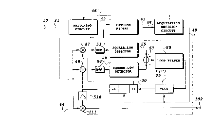
Fig. 5 shows an embodiment of the present invention.
A received signal 21 applied to the input terminal 10 is
selectively supplied through a switching circuit 42 to an
initial acquisition circuit 43 consisting of a matched
filter or to a correlation detector 44. The initial
acquisition circuit 43 has an arrangement similar to that
of Fig. 1. The correlation detector 44 has a function
similar to the correlation detectors of Figs. 2 and 3.
When the initial acquisition has not yet been completed,
the received signal is supplied to the initial
acquisition circuit (matched filter) 43 in accordance
with a switching signal 46 from an acquisition decision
circuit 45, so that the correlation detection is
performed. The correlation value detected by the matched
- 32 -
CA 02276200 1999-07-19
i
filter 43 is compared with a threshold value in the
acquisition decision circuit 45. If the correlation
value is greater than or equal to the threshold value,
the acquisition~decision circuit 45 decides that the
initial acquisition has been completed, and changes the
switching circuit 42 using the switching signal 46.
Thus, the received signal is inputted to multipliers 47
and 48 in the correlation detector 44. The acquisition
decision circuit 45 provides an initial reset signal 49
to a VCCG 29 and a spreading code replica generator 30.
The received signal 21 after the initial acquisition
is multiplied by spreading codes 51 and 52 by the
multipliers 47 and 48, the spreading codes being
generated by the spreading code replica generator 30, and
having phases shifted forward and backward in time by an
amount~T (less than one chip interval). The two products
are passed through bandpass filters (BPF) 53 and 54, and
are square-law detected by square-law detectors 55 and
56, in which correlation values are detected. The
correlation values are summed in the opposite phase by an
adder 57. The sum is passed through a loop filter 58,
and becomes a control voltage of the VCCG 29. The clock
signal generated by the VCCG 29 regulates the phase of
- 33 -
CA 02276200 1999-07-19
the spreading code replica generator 30,, tracks the
synchronous point, and maintains the synchronization.
Fig. 6 illustrates an example, in which the
spreading code replica generator 30I is synchronized with
the outputs of the quadrature detector 62 which detects
the received signal 21 applied to the input terminal 10.
In this figure, portions corresponding to those of Fig. 5
are designated by the same reference numerals. Suffixes
I and Q are attached to the same numerals as in Fig. 5 to
represent processing circuits of the two detected outputs
I and Q of the quadrature detector 62. The detected
outputs I and Q are passed through lowpass filters 63 and
64, converted into digital signals by A/D converters 65
and 66, and supplied to switching circuits 42I and 42Q.
The outputs of the initial acquisition circuits 43I and
43Q are square-law detected by square-law detectors 71
and 72, summed by an adder 73, and supplied to the
acquisition decision circuit 45 which decides whether the
initial acquisition is established or not.
A spreading code replica generator 30I in the
correlation detector 44 generates an advanced spreading
code 51I with an advanced phase and a retarded spreading
code 52I with a retarded phase. Likewise, a spreading
- 34 -
CA 02276200 1999-07-19
code replica generator 30Q generates an advanced
spreading code 51Q with the advanced phase and a retarded
spreading code 52Q with the retarded phase. The detected
output component I outputted from the switching circuit
42I is multiplied by the advanced spreading code 51I and
the retarded spreading code 52I by multipliers 47I and
48I. Likewise, the detected output component Q outputted
from the switching circuit 42Q is multiplied by the
advanced spreading code 51Q and the retarded spreading
code 52Q by multipliers 47Q and 48Q.
The detected correlation values with the advanced
spreading codes 51I and 51Q, which are outputted from the
multipliers 47I and 47Q, are passed through bandpass
filters (BPFs) 53I and 53Q, square-law detected by
square-law detectors 55I and 55Q, and are summed by an
adder 6.7. Similarly, the detected correlation values
with the retarded spreading codes 52I and 52Q, which are
outputted from the multipliers 48I and 98Q, are passed
through bandpass filters (BPFs) 54I and 54Q, square-law
detected by square-law detectors 56I and 56Q, and are
summed by an adder 68. The outputs of the adders 67 and
68 are summed in the opposite phase by the adder 57.
These operations are similar to those of~Fig. 5.
- 35 -
CA 02276200 1999-07-19
According to the first embodiment, the
synchronization process is separated into an initial
acquisition process, and a tracking process using the
correlation detector. The input PN sequence is acquired
so that the phase difference between the input PN
sequence and the reference PN sequence is settled within
a range sufficiently smaller than t one chip interval
during the initial acquisition because the
autocorrelation of the PN sequence is established only
within a range of f one chip. The tracking processing
holds the phase difference between the input PN sequence
and the reference PN sequence within the range.
EMBODIMENT 2
Fig. 7 is a block diagram of a correlation detector
of a second embodiment. In Fig. 7, the same functional
blocks are designated by the same reference numerals as
in Figs. 1 - 6. As shown in Fig. 7, a signal applied to
the input terminal 10 is quasi-coherent detected by a
detector 104 using a local signal generated by a local
oscillator 103. The local signal has a fixed frequency
substantially equal to the center frequency of the
modulated signal. The correlation detector includes
- 36 -
CA 02276200 1999-07-19
multipliers 47 and 98 for detecting correlations between
the received spreading code and replicas of the spreading
code; bandpass filters 83 and 84 for extracting only
correlation detection signals from the products; a
carrier frequency error compensator 208 for compensating
the filtered output signals with a carrier frequency
error signal detected by an automatic frequency control
circuit; an adder 57 for summing in the opposite phase
the correlation detection signal associated with an
advanced phase replica and the correlation detection
signal associated with a retarded phase replica; a loop
filter 58 for averaging the phase error of the
correlation detection; a multiplier 111 for performing
correlation detection using a replica in phase with the
spreading code included in the received signal; an
integral-dump circuit 112 for integrating the output
signal of the multiplier 111 over M chip intervals; an
automatic frequency control circuit 213 for detecting the
carrier frequency error from the output signal of the
integral-dump circuit to compensate the carrier frequency
error; a demodulator 113 for making decision of the
received data after compensating the received phase error
of the signal obtained by the correlation detection; a
- 37 -
CA 02276200 1999-07-19
multiplier 119 for performing inverse modulation of the
decided data using the phase error signal outputted from
the loop filter; a voltage controlled clock generator 29
for controlling the clock phase by the phase error signal
outputted from the multiplier 114; and the spreading code
replica generator 30 driven by the clock signal outputted
from the voltage controlled clock generator 29.
The modulated signal, which is down-converted by the
fixed oscillation frequency substantially equal to the
center frequency of the modulated signal, is deprived of
harmonic components, and is multiplied by the replica of
the spreading code in phase with the spreading code in
the modulated signal, followed by a predetermined length
of time integral. Thus, correlation peaks are detected.
The correlation detection signal undergoes decision by
the demodulation circuit which performs coherent
detection or delay detection. On the other hand, the
modulated signal is multiplied by the replica of the
spreading code with an advanced phase O with respect to
the spreading code in the modulated signal, and also
multiplied by the replica of the spreading code with a
retarded phase 0, thereby eliminating the harmonic
components.
- 38 -
CA 02276200 1999-07-19
The error signals between the correlation associated
with the advanced phase replica of the spreading code and
the correlation associated with the retarded phase
replica of the spreading code are added in the opposite
phase by the adder 57, and its output is integrated and
averaged by the loop filter 58. This results in an error
voltage corresponding to the phase error between the
spreading code in the received signal and the replica of
the spreading code. Inverse modulation by multiplying
the error voltage by the decided data outputted from the
demodulator eliminates the error in the phase error
signal due to the modulated signal. A delay is inserted
after the phase error detection loop in order to match
the absolute times of the processings of the phase error
detection loop and the data decision loop.
Ira the conventional DLL, a despread signal includes,
a phase error signal component that is a component of an
error between the center frequency of the received signal
and the frequency of the local oscillator of the
quadrature detector. The despread signal also includes
data modulation components and vestigial components of a
carrier signal component. To eliminate the carrier
frequency offset component and the data modulation
- 39 -
CA 02276200 1999-07-19
components, the despread signal may be squared by a
square-law detector. This, however, will increase noise
components because they are also squared, and the noise
components will be added to the chip phase error, thereby
increasing phase fitter.
Accordingly, it is necessary to obviate the square-
law detector to prevent the noise component from
increasing. In view of this, the present embodiment
eliminates the carrier frequency offset component from
the despread signal by the. AFC, and removes the data
modulation component by inversely modulating the
demodulated and detected signal into the despread signal.
Since the quasi-coherent detected signal includes a
carrier offset signal, the detected signal is involved
with phase rotations. Consequently, the carrier offset
signal-must be removed. This is achieved by detecting,
by the automatic frequency control circuit 213, the
offset component of the carrier signal from the
correlation peaks in the data decision loop, and by
correcting the two correlation detected signals of the
chip phase error detection loop by the carrier offset
signal in the opposite phase directions.
- 40 -
y
CA 02276200 1999-07-19
SUPPLEMENTS
Fig. 8 is a block diagram showing detailed hardware
of the correlation detector described in the second
embodiment. In this figure, the same elements are
designated by the same reference numerals as in Fig. 7.
In Fig. 8, the reference numerals 304 designates a 90-
degree phase shifter, 65 and 66 designate A/D converters,
308 and 309 designate complex multipliers, 313 designates
a delay circuit, 314 designates a complex multiplier, and
317 designates a decision circuit. The reference numeral
410 designates a carrier frequency error compensation
circuit, and 416 designates an automatic frequency
control circuit.
In the correlation detector, a received IF modulated
signal is quadrature-detected by the quadrature detector.
The quadrature-detected I and Q channel signals are
deprived of harmonic components, and are converted into
digital values by the A/D converters 65 and 66, followed
by the correlation detection by applying complex signal
processings on I (In-phase) and Q (Quadrature)
components. The correlation detection is carried out by
complex multiplication of the modulation spread signal by
the I and Q components of the replicas of the spreading
- 41 -
t
CA 02276200 1999-07-19
code. The two replicas of the spreading code is the same
if the in-phase and quadrature components of the primary
modulated signal are spread by the same spreading code.
The operation will now be described when the primary
modulation is QPSK and the secondary modulation is BPSK.
The data to be modulated are primary modulated
independently by binary data which are independently set
for I and Q channels (QPSK modulation). The I and Q
channel data are spread (secondary modulated) by the same
spreading codes. The input signal to the receiver is
expressed by the following equation.
Sit) - ~~(t - '~~)
Xfml(t - ~t) Sin[ewot + ee(t)J + mZ(t T ~~) Los[ewot + ee(t)]}
.. (16)
20
The signals after multiplying the input signal of
equation (3) by the replicas of the spreading code at the
receiver will be expressed as follows if a conventional
calculation method is applied.
- 42 -
CA 02276200 1999-07-19
r
y
E*(t) _
~K,~c(t - 2~)c(t - ~~ t 8){m,(t - ~t~ sin~Awot + 08(t)
+m2(t - ~~) cos~Awat + ~8(t)~)
'f'~Km[C(t - ~c~C~t - ~c ~ s~ - C~t - ~c)C(t - '~c f s~~
x{ml(t - ic) sin~Awot + DA(t)~ + m2(t - Tc) cos~Awot + 09(t)
+K,~C(t - Tt t 8)nj(t)
(17)
The chip phase error signal at the output of the loop
filter is expressed by the following equation.
e(t) = Y?(t) - Y.(t) = SKm~Inl Z(t - ~ct)}
+I12 2(t - 'tt~D~~c) + RmIle(t, E)
(18)
As shown by equation (18), since modulated signal powers
of individual symbol components are multiplied by the
phase error signal in the primary QPSK modulation, the
primary modulated signal components can be eliminated by
inversely modulating the I and Q components of the data
after decision into the phase error signal.
- 93 -
CA 02276200 1999-07-19
INDUSTRIAL APPLICABILITY
As described above in detail, according to the
present invention, the correlation detection during the
acquisition phase which requires a high speed
synchronization is carried out in the initial acquisition
circuit using a matched filter, and the correlation
detection during the tracking phase which requires power
saving rather than high speed synchronization is
performed by the sliding correlation detector. This
makes it possible to achieve the high speed acquisition,
and power saving during the tracking because the power
consumption of the initial acquisition circuit during the
tracking is negligible.
In addition, according to the present invention,
since the tracking loop of the received chip phase
eliminates the primary modulated signal components which
are included in the phase error signal of the replica
signals, components only depending on the
crosscorrelation can be extracted. This makes high
accuracy tracking possible.
_ 44 _