Note : Les descriptions sont présentées dans la langue officielle dans laquelle elles ont été soumises.
CA 02281343 1999-09-03
TITLE
Method and Apparatus for Cascading Frequency Doublers
FIELD OF INVENTION
This invention relates to a method and an apparatus for multiplying the output
frequency of an oscillator, and is particularly concerned with cascading
frequency
doubters to provide frequency sources in the microwave and millimeter-wave
frequency
bands.
BACKGROUND OF THE INVENTION
Emerging high-data-rate wireless communication systems in the Ka band, require
highly-stabilized, low phase-noise signal sources, and the phase-locked
oscillator (PLO) is
considered a promising candidate. The construction of millimeter-wave PLOs,
however,
necessitates a complex circuitry consisting of several radio frequency (RF)
components,
often resulting in a cumbersome packaging and high total cost along with high
DC power
consumption. Recently, millimeter-wave injection-locked oscillators have been
investigated to exploit low-GHz synthesizer sources comprised with low-cost
ICs, as
reported in:
Kamogawa et al., "Injection-locked oscillator chain: a possible solution to
millimeter-
wave MMIC synthesizers," 1996 IEEE MTT-S Symposium Digest, pp. 517-520; and
Suematsu et al., "Millimeter-wave HBT MMICs synthesizers using sub-
harmonically
injection-locked oscillators," 1997 IEEE GaAs IC Symposium Digest, pp. 271-
274.
These methods, using high multiplication factors, are also an attractive means
of
attaining better performance because the phase noise deterioration for
frequency
multiplication varies according to f2, while the phase noise of microwave and
millimeter-
wave oscillators reportedly degrades according to f -fs, as indicated in:
Isota et al., "Overview of millimeter-wave monolithic circuits," 27th European
Microwave Conference Proceedings, pp. 1316-1322 (Sept. 1997).
As an alternative to millimeter-wave PLOs, frequency multipliers have been
conventionally employed following microwave PLOs. In order to achieve higher
orders of
multiplication, frequency multipliers are often constructed with chains of
frequency
CA 02281343 1999-09-03
doublers because frequency doubling has been preferred for its higher
conversion
efficiency. In such multipliers, diodes have been conventionally used as
devices for
frequency conversion, and is required the insertion of driving power
amplifiers between
doublers to compensate for the conversion losses accompanied by frequency
multiplication.
Although possible conversion gain is expected by using transistors such as
field-effect
transistors (FETs), interstage amplifiers have been needed in high frequency
ranges such
as millimeter-wave frequencies where small-power devices have been used as
reported in:
H. Wang, et al., "A W-band source module using MMICs," IEEE Trans. Microwave
Theory Tech., Vol. MTT-43, No. 5, pp. 1010-1016, May 1995.
Depending on the capabilities of the devices and the operating frequency,
frequency
doublers have been cascaded without driving amplifiers as reported in:
Ninomiya et al., "60-GHz transceiver for high-speed wireless LAN system," 1996
IEEE MTT-S Symposium Digest, pp. 1171-1174; and
Hamada et al., "60 GHz phase locked oscillator using frequency doubler", 1997
IEICE Spring Conference C-2-45.
However, in these systems, each stage has been an independent circuit whose
input/output
impedances are matched to 50 ohms at the respective frequencies.
A configuration of cascaded frequency doublers in accordance with the prior
art is
illustrated in Figure 1. A first-stage frequency doubter 1 contains in a
series connection a
first input matching network la to provide 50 ohm matching for the
fizndamental
frequency signal, a first transistor lb, a first quarter-wavelength open-ended
stub lc for
suppressing the fiuldamental frequency, followed by a first output matching
network 1 d to
provide 50 ohm matching for the second harmonic frequency signal. A second-
stage
frequency doubter 2 contains in a series connection a second input matching
network 2a to
provide 50 ohm matching for the second harmonic frequency signal, a second
transistor
2b, a second quarter-wavelength open-ended stub 2c for suppressing the second
harmonic
frequency, followed by a second output matching network 2d to provide 50 ohm
matching
for the fourth harmonic frequency signal. US patent 4,754,229 issued to
Kawakami and
Kudo on June 28, 1988 describes a microwave design of a matching circuit
having similar
components to those shown in Figure 1.
The configuration shown in Figure 1 consists of cascaded frequency doubters
where
2
CA 02281343 1999-09-03
each stage is designed independently so that input/output impedances at each
stage is
matched to provide 50 ohm termination for its corresponding frequency. As a
consequence, different stubs are required for matching to 50 ohm in each
input/output
impedance matching network. Since relatively small-power devices are used, the
power
level is at most approximately 0 dBm. Employing medium-power transistors for
increasing the driving power level results in the frequency bandwidth becoming
narrower.
This is because the input resistance of medium-power transistors, which is
originally
relatively low, is often even further lowered by a quarter-wavelength open-
ended stub for
suppressing the fundamental frequency, necessitating a larger transforming
ratio to 50
ohm. For instance, a GaAs-based 500 ~m PHEMT from Northrop Grumman Corporation
shows the input resistance of approximately S ohm, hence the transforming
ratio to 50
ohm is about 10. This ratio can become equivalently even higher by the effect
of the
quarter-wavelength open-ended stub. In the case of such large ratios, an
additional
impedance matching network may need to be employed if the circuit is to be
terminated to
50 ohms with a sensible frequency bandwidth.
SUMMARY OF THE INVENTION
It is an object of the present invention to provide a method and an apparatus
for
multiplying the output frequency of an oscillator in low-frequency microwave
bands.
It is another object of the invention to provide a highly stable, low-phase-
noise local
frequency source in microwave and millimeter-wave frequency bands.
Therefore, in accordance with an aspect of the present invention, there is
provided a
method of frequency multiplication comprising the steps of
(a) receiving an input signal having a fundamental frequency component fo;
(b) providing an input impedance matching to said fundamental frequency
component;
(c) performing a plurality of n frequency doubling operations in series to
derive from the
input signal an output signal having an output frequency component of 2"fo,
wherein each frequency doubling operation, hereby referred to as a k' th
doubling
operation k<_n, includes the steps of
- receiving a k' th input signal having an input frequency component of 2~k-
l~fo,
- deriving from the k' th input signal a k' th intermediate signal having a
harmonic
frequency component of 2kfo,
3
CA 02281343 1999-09-03
- suppressing the input frequency component of 2~k-I~fo from the intermediate
signal;
and
(d) providing an interstage impedance matching to the harmonic frequency
component
of 2kfo between each pair of consecutive k' th and (k+1)'th frequency doubling
operations;
and
(e) providing an output impedance matching to the output frequency component
of 2°fo.
Preferably, each doubling operation step further includes a step of signal
stabilization after
the step of receiving said input signal.
In accordance with another aspect of the present invention there is provided a
multistage frequency multiplier comprising in a series configuration:
(a) an input network for receiving an input signal having a fundamental
frequency
component of fo and for providing impedance matching to said fundamental
frequency
component;
(b) a plurality of n frequency doublers, to derive from the input signal an
output signal
having an output frequency component of 2°fo,
wherein each frequency doubler, hereby referred to as a k' th doubler k_<n,
comprises
- means for receiving a k' th input signal having an input frequency component
of
2~k-l~fo, and deriving from said input signal a k' th intermediate signal
having a harmonic
frequency component of 2kfo, and
- means for suppressing said input frequency component from the intermediate
signal;
(c) a plurality of n-1 interstage networks, each positioned between a pair of
adjacent k'
th and (k+1)'th frequency doublers to provide an interstage impedance matching
to the
harmonic frequency component of 2kfo; and
(d) an output network for impedance matching to the output frequency component
of
2°fp.
In one embodiment of this invention, n=2 such that when a fundamental
frequency
signal is applied to the input network means, a fourth harmonic signal is
provided by the
output network means. In another embodiment, n=3 such that when a fundamental
frequency signal is applied to the input network means, an eighth harmonic
signal is
provided by the output network means.
In an embodiment of this invention, the frequency doubler comprises a three-
terminal
transistor device, which can be either a field effect transistor (FET) or a
high electron
4
CA 02281343 1999-09-03
mobility transistor (HEMT). Preferably, the suppressing means is a quarter-
wavelength
open-ended stub positioned from the transistor device output terminal by an
electrical
length suitable to provide a most effective suppression of the input frequency
component
of 2~k-l~fo and a most effective generation of the harmonic frequency
component of 2kfo.
Practically, in many cases the electrical length is substantially zero. Also
practically, the
transmission line is a microstrip line which has electrical parameters which
include
characteristic impedance and electrical length, that are so selected as to
achieve interstage
impedance matching by making a pair of reflection coefficients thereof seen in
opposite
directions to one another have phases of substantially the same values and
opposite
polarities. Optionally the characteristic impedance is substantially 50 ohms.
Yet another
embodiment of this invention further comprises stabilization means at the
input port,
preferably formed of a shunt resistor.
This invention provides interstage matching within a multistage frequency
multiplier,
without a need for driving amplifiers between doubters therein. One advantage
of the
present invention is to simplify the circuit topology because the stubs for
impedance
matching are eliminated, resulting also in a reduction in the total size of
the circuits.
Another advantage is that when a cascading doubter uses medium power three-
terminal
transistors, drive power levels can be increased keeping the bandwidth from
getting
narrow, thereby providing the output power level required from a local
oscillator. The
apparatus and method of the invention are of particular use in high-speed,
large-capacity
communications systems and in microwave and millimeter-wave radar
transmitters.
BRIEF DESCRIPTION OF THE DRAWINGS
Exemplary embodiments of the invention will now be further described with
references to the drawings wherein:
Figure 1 shows a prior art frequency multiplier consisting of two frequency
doubter
stages;
Figure 2a illustrates in a block diagram a three-stage frequency multiplier
configuration using two interstage networks in accordance with the present
invention;
Figure 2b shows the elements of each of the interstage networks used in an
embodiment of the configuration of Figure 2a;
Figure 3 shows in a circuit diagram the three-stage frequency multiplier
illustrated in
5
CA 02281343 1999-09-03
Figure 2a;
Figure 4a illustrates in a graph measured fourth harmonic output power versus
angle
between two frequency doublers in accordance with the invention;
Figure 4b illustrates in a graph measured fourth harmonic output power and
conversion gain versus input power in a two-stage multiplier in accordance
with the
invention;
Figure 4c illustrates in a graph measured fourth harmonic output power versus
fundamental frequency.
Figure 5 illustrates in a graph the suppression of unwanted harmonics in a two-
stage
multiplier embodiment of this invention; and
Figure 6 illustrates in a graph eighth harmonic output power and conversion
gain
versus input power for the three-stage multiplier of Figure 2b.
DETAILED DESCRIPTION OF THE INVENTION
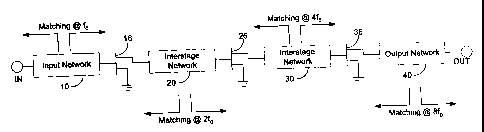
Figure 2a illustrates in a block diagram the operating principles of a three-
stage
frequency multiplier configuration using two interstage networks in accordance
with the
present invention. The multiplier contains in a series configuration an input
network 10, a
first transistor 16, a first interstage network 20, a second transistor 26, a
second interstage
network 30, a third transistor 36, and an output network 40. Each of the four
networks 10,
20, 30 and 40 provides an impedance matching for its corresponding frequency,
i.e. the
fundamental frequency fo, the second harmonic 2fo, the fourth harmonic 4fo,
and the eighth
harmonic 8fo, respectively.
In general terms, a multistage frequency multiplier is stated as to include a
plurality of
n frequency doublers, to derive from the input signal an output signal having
an output
frequency component of 2°fo, and each frequency doubler is then
referred to as a k' th
doubler k_<n, which receives a k' th input signal having an input frequency
component of
2~k-l~fo, and derives from it a k' th intermediate signal having a harmonic
frequency
component of 2kfo.
Figure 2b shows the elements of an embodiment of each of the interstage
networks
20 and 30 used in the configuration of Figure 2a. Such an interstage network
consists of a
quarter-wavelength (~,/4) open-ended stub 1 for suppressing the main input
signal
component, coupled to a transmission line 2 including a DC block capacitor 3.
A shunt
6
CA 02281343 1999-09-03
resistor 4 coupled to the gate 5 of a frequency doubling transistor device 6
is used for
stabilization when the input resistance of the next stage doubler is either
close to zero or
negative. The transistor device 6 is a three-terminal transistor biased in
such a manner as
to exploit its nonlinearity for the purpose of generating a second harmonic
frequency. In
this embodiment, the transistor device 6 is a field effect transistor (FET) or
a high electron
mobility transistor (HEMT), but other types can also be used, such as
heterojunction
bipolar transistors (HBTs). Impedance matching between the transistor devices
of two
successive stages is made by selecting the appropriate characteristic
impedance of the
transmission line 2 and its electrical length, to provide the required
interstage conjugate
impedance matching. In this embodiment, the transmission line 2 is formed of a
microstrip line, but other transmission lines can be used, such as coplanar
waveguides.
Although there is not much significance in their directions, the open-ended
stubs 1 for
impedance matching are indicated in the figures as pointing upwards, whereas
the stubs
for suppressing the input signals shown as pointing downwards. An open-ended
stub is
defined herein as a transmission line section that ends in an open circuit.
Also shown in Figure 2b is a transmission line section 7 positioned between
the
preceding transistor 6' and the open stub 1, indicating that the input-signal
suppression
stub is placed at a distance from the drain 8 of the preceding transistor 6'.
However, this
section 7 is not necessarily required for all embodiments. In many cases the
open stub 1,
which is placed as close as possible to the drain 8 of the preceding
transistor 6',
successfully works as is the case in the embodiment shown in Figure 3. The
entire circuit
between the two successive transistor devices 6' and 6, including this section
7, work as
the interstage network 20. The interstage network 20 of Figures 2a and 2b
substitute for a
pair of inputloutput port matching networks 1 d and 2a shown in Figure 1.
This configuration is feasible with frequency doubters using (medium-) power
transistors, which can yield conversion gain at successive stages and maintain
the driving
power at sufficiently high levels. It is useful for multiplying the output
frequency of
phase-locked loop oscillators in order to provide highly stable, low-phase-
noise local
frequency sources in microwave and millimeter-wave frequency bands. This
apparatus is
also useful for multiplying the output frequency of voltage controlled
oscillators in order
to provide output signals from radar transmitters in microwave and millimeter-
wave
frequency bands.
7
CA 02281343 1999-09-03
In a preferred embodiment, the effect of using a shunt resistor 4 located on
the gate
of the transistor 6 as stabilization means was tested. Single stage frequency
doubters were
designed and fabricated for two frequency bands; 7.5/15 GHz and 15/30 GHz. The
shunt
resistor is monolithically integrated with transistor devices, here HEMTs, on
a single
semiconductor wafer along with other network elements such as transmission
lines and
capacitors. For instance, in the 7.5/15 GHz doubter, a 500-ohm resistor is
fabricated using
a resistive metallic thin film, which is 30 micron wide and 100 micron long.
This resistor
is shunted to the ground by a following capacitor and a "via" hole. This shunt
resistor was
found to reduce the magnitude of the voltage reflection coefficient, seen from
the gate to
the device, to 0.876. Then the input matching network is designed so as to
attain the
conjugate impedance matching. With this design, no oscillation was
experimentally
observed during the operation of the frequency doubters; thus the circuits are
well
stabilized.
Figure 3 shows an embodiment of a three-stage frequency multiplier
configuration in
accordance with the invention. This consists of an input-port matching network
10 for the
fundamental frequency, first and second interstage matching networks 20 and 30
for the
second and the fourth harmonic frequencies respectively, and the output-port
matching
network 40 for the eighth harmonic frequency. Open-ended stubs 19 and 49 are
used for
the input-port matching network 10 and the output-port matching network 40,
respectively. The shunt resistor 4 shown in Figure 2b is not used in this
embodiment. A
characteristic impedance of 50 ohm is used for the interstage transmission
line.
The value for capacitors 23 and 33 is chosen so as to be close to short
circuited for the
radio frequencies being considered. In this embodiment, 10 pF chip capacitor
is used due
to its comparable size with the transmission line width, although its
impedance is several
ohms for the fundamental frequency (for the higher-order harmonics, the
impedance gets
close to 0 ohm) and the effect is taken into account for design. The length of
stubs 21, 31
and 41 is approximately a quarter of the corresponding wavelength
(fundamental, second
and fourth harmonics respectively), where the term "wavelength" is used to
refer to the
effective wavelength, the geometrical structure of the microstrip line taken
into account.
In order to achieve efficient frequency doubling, the transistor is biased
either near
the forward conduction point or the pinchoff, where the device behaves as a
half wave
rectifier. The pinchoff bias operation is adopted for less DC power
consumption, and
8
CA 02281343 1999-09-03
also for keeping lower frequency harmonics from being amplified. When the bias
voltage at the gate of each transistor is kept below the pinchoff bias, the
channel between
the source and the drain is entirely blocked, hence no current flowing through
the
respective drain-to-source channel. Then with a sinusoidal input signal, the
transistor is
tuned on only during the positive half cycles of the drive waveform, thereby
generating
a second-harmonic frequency component efficiently.
In a preferred embodiment, the apparatus includes microstrip lines on 250-~cm
thick
Alumina substrates mounted on metallic carriers. Medium power devices used are
FujitsuT"" FSX52X, commercially available 600-pin MESFET, for the first-stage
doubler, and GaAs-based 500 ~,m PHEMTs from Northrop Grumman Corporation for
the second and third stage. This design is based on the small-signal
scattering
parameters (S parameters), which are defined by the ratios of the incident
wave over the
reflected wave. For example, in the case of 2-port networks having of an input
port and
an output port, a scattering parameter S11 is defined as the ratio of the
reflected wave to
the incident wave at the input port, when the output port is terminated to the
characteristic impedance of the transmission line. Similarly, another
scattering
parameter S22 is defined as the ratio of the reflected wave to the incident
wave at the
output port when the input port is terminated to the characteristic impedance
of the
transmission line. These parameters are often referred to as "small-signal" in
comparison with large-signal behaviors where nonlinear phenomena dominate.
Small-
signal S parameters for designing multipliers, which make use of nonlinear
behaviors,
are often used in a preliminary approach when large-signal characteristics of
devices are
unknown. On the output side of each transistor device is placed a quarter
wavelength
open-ended stub for suppressing the input frequency signal to each stage. Each
transistor device is biased at pinchoff for the efficient second harmonic
generation.
Because of the quarter wavelength open-ended stub being connected on the
output side of
the transistor device, S11 for the input frequency, seen from the gate toward
the
transistor, changes to S1,' in accordance with the following formulas:
Su'=Sn+O
0 = S12S2irL/(1-S22rL)
I'L = -exp (-j29).
9
CA 02281343 1999-09-03
Here, 8 is the electrical length from the drain to the position where the
quarter wavelength
open-ended stub is located. When the angle arg (0) happens to be close to the
angle
arg (S11), then the magnitude ~511'~ becomes maximum. This magnitude could be
close to
or more than unity for medium-power FETs, whose input impedance is relatively
small
and hence ~511~ is relatively large. For instance, ~511~ of the FSX52X device
is 0.871 at a
fundamental frequency fo of 3.5 GHz, while ~511'~ is increased to 0.949 when 0
is
substantially zero. Similarly, ~S1 y of the Northrop Grumman 500 pm PHEMT
device is
0.937 at the second harmonic frequency 2fo of 7 GHz, while ~511'~ is 1.003.
~SII~ at the
fourth harmonic frequency 4fo of 14 GHz, of the same device is 0.921 and its
~SI1'~ is
1.054. Here, ~S22~ for the preceding device is sufficiently smaller than unity
and yet not
significantly different from ~511~; ~Sz2~ of the Northrop Grumman PHEMT device
is 0.782
at 7 GHz and is 0.839 at 14 GHz. In this embodiment, leaving the magnitudes as
they are,
the phases of the reflective coefficients are matched by selecting the
appropriate electrical
length of each interstage section which consists of transmission lines with 50
ohm
characteristic impedance and a DC block capacitor. The above S parameters are
based on
the typical measured data of each indicated type of transistor devices, which
are acquired
through the measurement of several devices from each type. Large-signal
characterization of the Northrop Grumman devices was also made using automatic
mechanical tuners, which were placed on the input and output terminals; they
were varied
while a large-signal incident wave was applied, and thus the input and output
impedances
were tuned so that the most efficient second harmonic generation would be
obtained. The
magnitudes of the large-signal S11 and S22 for 14 GHz, evaluated to correspond
to the
optimum impedances, were found to be smaller than those of small-signal
parameters, and
this is a favourable condition in terms of stabilization.
A suitable non-zero value of the electrical length 0 is one that provides a
most
effective suppression of the input frequency component of 2~k-l~fo and a most
effective
generation of the harmonic frequency component of 2kfo. This is done using
known
approaches such as described in:
C. Rauscher, "High-frequency doubter operation of GaAs field-effect
transistors,"
IEEE Trans. Microwave Theory Tech., vol. MTT-31, pp. 462-473, June 1983.
In practice, however, a substantially zero value of 8 for pinchoff operation
is found to
be suitable, which means the drain is short-circuited for the input frequency
component.
CA 02281343 1999-09-03
The following provides a general expression for determining the appropriate
electrical
parameters of the transmission line section in terms of its characteristic
impedance and
electrical length between the k' th and the (k+1)'th device. Suppose the
output impedance
of the k' th device for the harmonic frequency of 2kfo, fo being the
fundamental frequency,
is expressed by Rk+ jXk, and the input impedance of the (k+1)'th device for
the same
frequency is expressed as Rk+1 +JXk+1, then the appropriate characteristic
impedance, Zk,
k+1, and electrical length between the k' th and the (k+1)'th device, Lk, k+1,
are expressed by
the following:
Zk, k+12 = (Xk2Rk+1 -Xk+l2Rk)/(Rk -Rk+1 ~ + RkRk+1 and
Lk, k+1 = (~g/2T~) ~Ctari ((Rk -Rk+1)Zk, k+1/(RkXk+1 -XkRk+1)O
where ~,g is the effective wavelength. Since "arctan" is a periodic function
with a period
of ~, it takes values from 0 to ~c when positive values are supposed,
resulting that Lk, k+1 is
at most 7~g/2. Since here Zk, k+1 is supposed to be a real number, these
formulas have a
solution only when the right hand of the first formula is positive. This value
becomes
negative for the Northrop Grumman PHEMT device at 14 GHz, for instance, hence
only
the phase was conjugately matched in this embodiment.
When the parameters of the interstage network are selected as above, the
circuit is
conjugately matched for the harmonic frequency of 2kfo. Suppose that the
impedance,
seen from a point on the interstage network to the direction of the n'th
device is expressed
by Zo"t, k, and the impedance network to the direction of the (k+1)'th device
is expressed
by Z;", k+1, this matching condition is then expressed by Zo"t,k = Z;n, k+1 *.
This is good at
any point on the interstage network. If we express using reflection
coefficients, then Szz,
k = 511, k+1*. In polar presentation, X522, k~ _ X511, k+1 ~ and arg (522, k)
_ - ~'g (511, k+1).
Although what is described above provides a general approach, a preferred
embodiment is so designed that only the phase conjugate condition,
arg (522, k) _ -~'g (511, k+1) is valid. In other words, the phases of the
reflection coefficients
seen in opposite directions have the same values but with the opposite
polarities. The
magnitude of Zk, k+1 is chosen as 50 ohm and the lengths as L1,2 = 0.310 ~,g
and
L2,3 = 0.137 7~g. An extra section having a length of 0.5 ~,g is added to the
second
interstage network just for the convenience of MIC fabrication.
A frequency quadrupler embodiment (not shown) with two stages of frequency
doubling was constructed for testing purposes from an input matching network
for the
11
CA 02281343 1999-09-03
fundamental frequency, and two interstage matching networks as described above
(the
second interstage network does not work as such for here). The two stages of
frequency
doubling were provided with only a fundamental frequency suppression stub on
their
output port. During testing of the doubling circuits, a phase shifter was
placed between
the two circuits, and the phase angle was mechanically varied. The fourth
harmonic
power varied by 9 dB with a period of 180 degrees as shown in Figure 4(a).
Here, the
fundamental frequency is 3.6 GHz and the input power is 6 dBm. The phase
difference
between the angles which gave 1 dB less output power than the maximum level
was 25
degrees. This relatively phase-insensitive feature is advantageous for design.
The tested
quadruples embodiment, incorporating interstage impedance matching, had a
14.25 GHz
output freguency. Measured fourth harmonic output power and the conversion
gain of this
quadruples is shown in Figure 4b as a function of input power. A maximum
conversion
gain of 13.8 dB was obtained for an input power of -1 dBm. Figure 4(c) shows
the fourth
harmonic power as a function of the fundamental frequency when the input power
is 1.5
dBm. The output power is reflected by the frequency dependency of the
measurement
system which is illustrated in Figure 4c. The variation would be less when the
system is
calibrated. As shown in Figure S, with a vertical scale of 10 dB per division
indicated at
the top of the figure, the unwanted harmonics were suppressed to less than -
40dBc
compared to the fourth harmonic, except for the second (-27dBc) and the fifth
(-35dBc)
harmonics. This two-stage frequency multiplier, although having the output
matching
network omitted, exhibited a pretty good performance. With an output matching
stub as
described above, the performance is expected to be even better. When a third
transistor
device and an output-port matching network for the eighth harmonic is combined
with this
quadruples, a three-stage multiplier is obtained. Measured eighth harmonic
output power
versus input power for such a combination is shown in Figure 6. The preferred
multiplier
shows a maximum conversion gain of 6.1 dB for the input power of -3 dBm. The
output
power of 4.3 dBm was obtained for 0 dBm input power. The total DC power
consumption
was 257 mW when the input power is 2 dBm. Since the input power to the third
transistor
device is more than 10 dBm, the networks related to the third frequency
doubling, i.e. the
second interstage network and the output matching network, are not properly
realized
when designed using small-signal S parameters. The performance is expected to
be even
better by incorporating large-signal parameters.
12
CA 02281343 1999-09-03
Of course, numerous variations and adaptations may be made to the particular
embodiments of the invention described above, without departing from the
spirit and
scope of the invention, which is defined in the claims.
13