Note : Les descriptions sont présentées dans la langue officielle dans laquelle elles ont été soumises.
CA 02282391 1999-08-24
Circuit Arrangement and Method for Supplying Pulse Current to
Electroplating or Etching Systems v
Specification
The invention relates to a circuit arrangement arid a method for supplying
pulse
current to one or more electrolytic cells which are connected in parallel. The
method is preferably used for the electroplating of printed rarcuit boards in
vertical dipping systems and in vertical and horizontal feed-through systems.
Electroplating by means of pulse currant makes it possible to influence
certain
properties of the metallic layers which are deposited. In this way, the
physical
properties of the electroplate layers can be altered within wide limits. In
particular, throwing power is improved. fn addition, the nature of the surtace
can be influenced. What is also particularly advantageous is that the
resulting
electroplating current density and the product quality can be considerably
increased. But against the advantages in relation to the product to be
electroplated is sat the disadvantage of the outlay on equipment for the
generation of the pulse current. The systems used for supplying the pulse
current come Quickly up against physical, technical and economic limits if the
electroplating is to be done with current pulses which are brief. As
"brief° are to
be understood here pulse times in the region of 0.1 ~10~ to 10 ~10'' seconds.
It
is in this time range that electroplating by means of pulse cun-ant is
particularly
effective. Where bipolar pulses are used, the artiGe to be treated is
polarised
alternately cathodically and anodically. If the article for treatment is to be
electroplated, the cathodic current~time product (cathodic charge) must be
greater than the anodic current/time product (anodic charge).
The advantages of pulsed electroplating can also be used in the electrolytic
treatment of printed circuit boards. Vertical and hori2ontal electroplating
systems are used in the manufacture of printed circuit boards. Systems of this
kind are generally of very large spatial dimensions. Furthermore, the
CA 02282391 1999-08-24
2
electroplating currents are large in this case. For this reason, galvanic
rectifiers
with correspondingly high capacity must be installed in the electroplating
system.
Because there is practically always a lack of space, it is often not possible
for
the galvanic rectifiers with the pulse generators to be positioned very close
to
the electroplating tanks. This is the opposite of what is r~Quired with the
application of pulsed technology: with known methods and systems, the
distance between the galvanic rectifier and the bath, i.e. the electrolytic
cell,
.i 10 must be very short in order to achieve the necessary edge steepness of
the
pulse currents. With the usual large pulse currents Ip and in the case of low
bath resistances Rp,~,, the inductance Lt of the conductors between the
galvanic rectfier and the electrolytic cell must be kept small. In practice
this
can only be achieved with very short electric lines. Further measures for
reducing the conductor inductance are known, such as for example the
transposition of forward and return conductors. This current conductor layout
is
admittedly possible with cables which have a small conductor cross-section.
On the usual conductor rails for high electroplating currents, on the other
hand,
transposition is impossible. The time constant Tau for the current rise in the
bath resistance Rb,~, is calculated according to the formula
Tau = L.~/R~,~,.
If the distance between the galvanic redfier with its pulse generator and the
bath is only, for example, three metres, with a conductor inductance of, for
example. 1 ~ 10'° Henry per metre this would be 6-10' Henry for the
forvvard and
return conductor.
If a value of R"~, = 310'' Ohm is assumed for the bath resistance, this gives,
with an admissible disregara of the ohmic conductor resistance, a time
constant
of
Tau = L~IR~"~, _ (6~10~' Henry)/(3~10'' Ohm) = 2~10''seconds.
CA 02282391 1999-08-24
3
Wlth an ideal voltage ris~ in the pulse generator the current in the bath
resistance Rte", thus rises within 210'' seconds to 63% of the maximum
current. The speed of this pulse rise is insufficient for circuit board
electroplating, for example. In that case the above-mentioned pulse lengths
are worked with. The pulse rise time must be correspondingly shorter.
A horizontal electroplating system for printed circuit boards consists for
example of twenty-five anodes connected in parali~! on the underside of the
circuit board and twenty-five anodes connected in parallel on the upper side
of
the circuit board. The pulse currents on each side are up to 15,000 amperes.
The dimensions of an electroplating system of this kind amount, for example,
to
six metres in the direction of transport. The current conductors from the
galvanic rectifier with its pulse generator to the anodes must be of a
corresponding length.
A usual system is shown diagrammatically in Fig. 1:
The circuit boards 1 to be treated are transported through the system in the
direction of the arrow, between the upper anodes 2 and the lower anodes 3 of
drive elements which are not shown. These anodes can be both soluble and
insoluble anodes. In a feed-through system of this kind, each anode forms with
its associated cathode (circuit board) and the electrolyte an electrolytic
partial
cell. By preference, all the upper anodes 2 form together with the upper side
of
the article to be treated and the electrolyte the upper electrolytic total
cell which
is supplied with bath current from the galvanic rectifier 5. Correspondingly,
the
lower anodes 3 form together with tt~e lower side of the article to be treated
and
the electrolyte the lower electrolytic total cell. Anodes 2. 3 are each
electrically
connected with a common upper galvanic rectifier 5 and a common lower
galvanic rectifier 6 via a switching contact 4. Because of the large size of
the
rectifier, the distance between the galvanic rectifiers 5, 8 and the
electroplating
system amounts in practice to at least a few metres. The current conductor 7
to the upper anodes and current conductor 8 to the lower anodes are of a
p"'' ,
CA 02282391 1999-08-24
4
corresponding length. The common current return conductor 9 closes the
circuits of the galvanic rectifiers. The article to be treated is connected to
electric line 9 by means of electrical contact elements, for example in the
form
of clamps 10 which are connected with'a slip rail 11 so as to slide and be
electrically conductive. The switching contacts 4, as a rule electro-
mechanical
contactors, serve to switch the anodes individually when the first conductor
boards are transported into the feed-through system and to switch off the
anodes individually when the last circuit boards are brought out of the feed-
through system or when gaps appear between the circuit boards. The function
. 10 of switching contacts 4 is described in DE-A,39 39 681. Reference is made
to
this document.
In traditional technology, the necessary high current rise speeds, in
conjunction
with the high currents in the current conductors from the pulse generator to
the
bath, cause severe magnetic disturbance fields. The admissible field strengths
for work in the surrounding field of such disturbenoe fields, are laid down in
corresponding standards. Safety measures for protecting the personnel who
operate the electroplating systems, as described for example in the German
standard VDE 0848, also have to be observed. For this reason, screening
measures are necessary which involve considerable technical outlay with
correspondingly high costs. Where the electroplating cun-ents ere very high,
even these measures are ineffective.
The described technical and economic problems with electroplating by means
of quick purses represent reasons why so far this pulse technology has not
been used in commercial production.
In WO 89/07162 A1, an eledro-chemical process is described which uses a
pulse method. With the reverse pulse method, at least one bath voltage source
in the forward direction, i.e. electroplating, and at least one further bath
voltage
source in the reverse direction, i.e. etching or depleting. is alternately
connected to the electrolytic bath. The adjustable voltage sources drive the
bath current. With voltage sources, the amplitude and the time response of the
CA 02282391 1999-08-24
current are dependent on the ohmic and inductive resistances of the bath
circuit. The voltage change-over and thus at the same time the generation of
current pulses in a forward and a reverse direction are realised by means of
solid state switches which are in the position of switching the necessary high
5 pulse frequency of up to 5,000 Hertz. In electroplating, the bath current
average value in the forward direction, i.e. with cat>hodic polarisation of
the
article to be ~Iectroplated, must be considerably larger than the bath current
average value in the reverse direction, i.e. with anodic polarisation. The
proposed switches for generating bipolar current pulses from two voltage
' 10 sources are not suitable far brief pulses in real electroplating systems.
The
current conductors from the voltage sources to the voluminous systems are so
long that, as a result of the correspondingly high conductor inductance, the
pulse rise speeds ere substantially greater than the necessary pulse length,
especially the reverse pulse length. This is true regardless of the place in
the
electroplating circuit at which the solid state switches are introduced, i.e.
connected in series.
What is also known is that, in switching off a current of an inductive charge,
an
induction voltage is produced with an amplitude which is dependent on the
switch~ff speed and the size of the inductance. This voltage is added to the
current sourcing voltage. The sum of the voltages is available at the opened
switch. Said switch is destroyed unless there are expensive protective
measures, especially with the usual high energies which are switched in
electroplating systems.
Known extinguishing circuits parallel to the inductance cannot be realised in
large electroplating systems. An extinguishing circuit would, in addition,
have
the disadvantage that the dying away of the current when switched off would be
sign~cantiy slower. A further disadvantage of the switches proposed proves to
be the necessity of installing very expensive protective measures against the
strong magnetic fields in the region of the current conductors.
The unavoidable conductor inductance in the bath circuit always has a
CA 02282391 1999-08-24
disadvantageous effect on pulse generation. Even experimentally it was not
possible with this technique to achieve pulse rise times with Tau smaller than
210'3 seconds. The outlay in order to protect the electronic switches and to
protect the personnel against the strong magnetic fields was
disproportionately
high in this case.
Thus the problem underlying the present invention is to avoid the
disadvantages of the known methods and circuit arrangements end especially
to indicate a method and a circuit arrangement for supplying pulse current to
~ 10 electrolytic cells, by means of which method pulse currents with a large
edge
steepness can be generated in large electroplating and etching systems with
one or more electrolytic cells, and with which at tha same tine the generation
of
electro-magnetic fields is limited to a minimum.
1:r The pmblom io oohed by !ho oW ouit orran~o.ront oaeaidin' !!~ !~~e~n~ ~
onri fho
methods according to claims 9 and 10. Prefen~ed embodiments of the invention
are given in the dependent claims.
In the circuit arrangement according to the invention for supplying pulse
current
20 to one or more electrolytic cells which are connected in parallel and have
anodes and cathodes, there are associated with each individual electrolytic
cell
a. at least one galvanic rectfier; and
b. at least one change-over switch which may be switched through from at
least two inputs to at least one output, or one on/off switch;
25 c. first electric lines for making a direct electrical connection between
respectively one terminal of the rectifiers and the one terminal of the
electrolytic cell: and
d. second electric lines for making a direct electrical connection between
the respective other outputs of the rectifiers and the inputs of the
30 change-over switches or a terminal of the on/off switch being provided;
and in addition
e. the output or the outputs of said at least one change-over switch or the
other terminal of the on/off switch being directly connected with the other
CA 02282391 1999-08-24
7
terminal of the electrolytic cell; and
f. at least one capacitor being connected between th~ first electric line and
each second electric line.
S With corresponding control of the change-over switches for the periodic
closing
and opening of the connections between the rectifiers and the electrolytic
cell
via the second electric lines, the following process steps are carried out
with
this circuit arrangement during electroplating or etching, partiwlarly
depleting:
A. In a first time interval t, (for example in order to generate a cathodic
current
pulse on the article to be treated (tk)):
a. by connecting a first rectifier with the electrolytic cell, said cell is
fed via a
second electric line and at least one change-over switch; and
b. simultaneously the capacitor or capacitors which are connected to the
first rec~:ifier via one of the second electric Nnes are partially discharged;
c. the capacitors, which are connected with the other rectfiers via the
remaining second electric lines are charged.
B. In a second time interval tz (for example to generate an anodic current
pulse
on the artiGe that Is to be treated (t.)):
d. by connecting a second rectifier with the electrolytic cell, said cell is
fed
via a second electric line and at least one change-over switch; and
e. simultaneously the capacitor or capacitors which are connected with the
second rectifier via another of the second electric lines are partially
discharged;
f, the capacitors which are connected with the remaining rectifiers via the
remaining second electric lines are charged.
In order to avoid the switches or other componenfis being destroyed, a
plurality
of rectifiers should not be connected with the electrolytic cell via the
switches at
the same time. For this reason, the known method "break before make" is
CA 02282391 1999-08-24
8
applied, according to which the connection between the electrolytic cell and a
rectifier is interrupted by a switch before a new connection is made between
the
cell and some other rectifier. In this way the galvanic rectifiers do not
short-
circuit one another. '
With the use of onloff switches the following method steps are carried out.
A. In a first time interval t, (for example for generating a cathodic current
pulse
on the article to be treated (tk)):
a. by connecting the rectifier or rectiFers with the electrolytic cell, the
electrolytic cell i5 fed via the second electric line and the oNoff switch;
and
b. the capacitors are simultaneously partially discharged.
B, In a second time interval tz (for example to generate an anodic current
pulse
on the article to be treated (t,)):
c. the connection between the electrolytic calf and tho rectifier or
rectifiers
is interrupted by the on/off switch; and
d. the capacitors are charged.
Through constant repetition of these process steps a-b-c-d-e-f or a-b-c-d, a
periodic current pulse sequence is generated in the electrolytic cell. Bipolar
pulse current is characterised by a sequence of positive and negative current
pulses. For certain applications, however, unipolar current pulse sequences
which only have cathodic or only anodic current pulses can also be generated
which, for example, respectively have different peak current values.
An arrangement which is formed by at feast one cathode and one anode, as
well as the electrolyte liquid situated between these iwo electrodes, can be
regarded as an electrolytic cell. Thus, in the manufacture of printed circuit
boards, on the one hand one side of a circuit board and the anode opposing the
same can, together with the respective electrolyte, be seen as an electrolytic
CA 02282391 1999-08-24
9
cell, and on the other hand the other side of the printed circuit board and
the
other anode facing same, together with the respective electrolytes, can be
seen
as another electrolytic cell.
Preferably, both the change-over switches and the on/off switches and the
capacitors are so arranged in relation to the electrolytic cell that the
inductance
of the current conductors connecting the electrolytic cell and the switches is
minimised. For example, the switches and the capacitors are arranged in close
proximity to the electrolytic cell by keeping this cement conductor as short
as
.10 possible. In addition, usual methods for optimising fhe wiring arrangement
can
be exploited in order to keep tfie conductor induetances to a minimum.
In a preterred embodiment, two rectifiers are provided with which a plurality
of
electrolytic cells, connected in parallel can together be supplied with
current, in
~ach case a plurality of circuits having common capacitors for supplying the
electrolytic cells. These circuits are preferably n~spectively allocated to
one
rectifier. This means that a group of several electrolytic cells is connected
via
the changeover switch with only one capacitor and this capacitor in turn is
connected with one rectifier. Another group of electrolytic cells is connected
via
the change-over switch or on/off switch with another capacitor and the latter
with another rectifier.
The group of electrolytic cells arranged on one side of circuit boards moved
on
a conveying path and consisting of circuit board surfaces facing this side,
the
anodes arranged on this side and the solution of electrolytes located between
these electrodes, can be connected as a group of electrolytic cells being
associated with a capacitor. The other group of electrolytic cells, which is
associated with another capacitor, is formed by the group of electrolytic
cells
situated on the other side of the conveying path.
In order to produce a low-maintenance circuit arrangement and high pulse
frequencies, for example of up to x,000 Hertz, electronic switches can be
provided to generate the pulse sequence. In principle, mechanical switches are
,~...
CA 02282391 1999-08-24
also possible. In that case, rotary switches and double-throw switches can be
used for the switches as well as circuits with a plurality of separate
switches
which are connected to one another in parallel and actuated attemately.
5 The change-over or offlon switches can respectively be equipped with a
current
sensor in order to control exactly the current intensity lecels in the
electrolytic
cells. The measuring signals which can be detected with these sensors are
also evaluated for excess current disconnection to protect the switches.
10 Th~ circuit arrangement according to the invention can, moreover, be
integrated into an electroplating or etching system in such a way that the
measuring signals of each current sensor can be transmitted to an higher-level
control which is contained in the electroplating and etching system and
provided to monitor and regulate same.
The change-over switches and on/off switches are preferably triggered by
means of electric control signals.
The amplitudes of the pulse currents flowing through the electrolytic cell are
preferably set at the given ratio of t, (for example tw: catholic current
pulse in
the first time interval) to tz (for example t, in the second time interval)
through
the adjustment of the catholic rectifier current I,, for the catholic
amplitude and
of the anodic rectifier current I, for the anodic amplitude.
Moreover, by measuring the amplitude values of the pulsed bath currents
flowing through the electrolytic cells and comparing these values with desired
values, the current amplitudes in the electrolytic cells can also be
controlled to
constant values by adjusting the rectifier current.
Additionally, further time intervals can also be introduced into the method
sequence a-tr-c-d-~--f or a-b-c--d, for example time segments in which no
current flows through the electrolytic cells, e.g. when the article to be
treated is
being taken in or out of the electrolyte solution. The change-over switches
ace,
CA 02282391 1999-08-24
11
to this end, so controlled that between time intervals t, and tz within a time
interval tx"a > 0 all connections between the rectifiers and the electrolytic
cell
ere interrupted.
By the change-over switch or the onlaff switch being triggered in a special
way,
certain method sequences can be realised. Moreover, the switching positions
respectively provided for the desired current direction of a change-over
switch
for supplying the electrolytic cell with direct current can be kept connected
whilst no current supply occurs via the respective other positions of the
switch
r~ 10 by the time intervals t, or tz on at least a portion of the electrolytic
cells being
set to such a size that the bath current acts as dir~ct current. The same
applies with the use of on/off switches.
1f a plurality of electrolytic cells are contained in an electroplating or
etching
system, said cells can be applied on in cycles with periodic current pulse
sequences. In a further form of embodiment, a plurality of groups of
electrolytic
cells can also be contained in the system, which are connected within a group
respectively parallel to one another. By preference in one group of these
electrolytic cells a first periodic current pulse sequence cam be generated
and in
another group of electrolytic cells a second periodic current pulse sequence
can be generated with a phase shift in relation to the first pulse sequence.
For
example, in a system for plating printed circuit boards, the electrolytic
cells
which are located on the one side of the printed circuit boards and the cells
which are located on the other side can respectively form different groups of
cells. In that case the electrolytic pulse currents are led to the individual
sides
of the printed circuit boards with phase shift. For example, at any given time
ll 'm. fm.,l .ri:Js.o of the r~ir.lsd eireui! 'os~de ee~ ~.o p~l.wiwe~
~~a~hnl~lir'9~~y
the rear sides simultaneously anodically, At a later point in time the
polarity is
then reversed.
In a further mode of operation, with for example separate circuits for the
supply
of the front and the rear sides of printed circuit boards, et least a portion
of the
electrolytic cells can be supplied by permanent interruption of the respective
CA 02282391 1999-08-24
12
connections between the rectifier and the electrolytic call, whilst a pulse
cun-ant
is led through the circuits of other electrolytic cells.
In order to avoid the separate switches being destroyed when they are opened.
diodes can, in addition, be connected parallel to the separate switches and be
of such polarity that when the separate switches are opened the energy which
is produced is taken up by the capacitors without any danger of destroying the
separate switches.
The invention is described in greater detail below with the aid of Figs. 2 to
5.
The figures show
Fig. 1 a diagrammatic view of the electrolytic partial cells in a horiZOntal
feed-through system according to the state of the art;
Fig. 2 the circuit arrangement according to the invention;
Fig. 3 an electrical equivalent circuit diagram of the circuit arrangement
according to the invention;
Fig. 4 time course of the currents and voltages during bipolar pulse
current supply with a current-controlled galvanic rectifier;
Fig. 5 time course of currents and voltages during bipolar pulse current
supply with a voltage-controlled galvanic rectifier.
The invention is shown by way of example in s horizontal feed-through system
for electroplating printed circuit boards. The circuit an-angement according
to
the invention end the method can also be used in a corresponding fashion for
etching printed circuit boards and for electroplating other articles.
Moreover,
the circuit and the method can also be used in vertical systems, for example
in
dipping systems or in systems in which the article to be treated is handled in
a
feed-through system in vertical orientation.
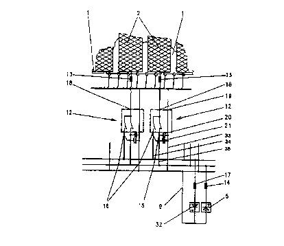
In Fig. 2 a system according to the invention is reproduced. Two upper anodes
2 and the article to be treated 1 are shown in detail. In the electrical
terminal of
the anodes 2, change-over switches 12 for bipolar pulse operation are
inserted.
CA 02282391 1999-08-24
13
The change-over switches 12 are arranged in proximity to the anodes. The
current conductor layout is chosen to be such that the current conductor
partial
inductance 13 from the output 18 of the change-over switch 12 to the
electrolytic cell is very small. On the other hand, the current conductor
partial
inductance 14, 17 of the galvanic rectifiers 5, 32 to the inputs 15, 1fi of
the
change-over switch 12 can be of any great size_
Below, the statement of the electrpplating phase always relates to the article
to
be treated 1. Accordingly, in the cathodic electroplating phase the article to
be
treated is polarised negativ~ly and the anodes positively. The anodic etching
or
depleting phase is fed from the galvanic rectifier 32 via the current
conductor
partial inductance 17. The associated change-over switch input has the
reference number 1 fi.
In the current conductor partial inductances 14 or 17, aN the effective
inductances of the circuits of the galvanic rectfiers 5, 32 to the inputs of
the
change-over switches 72, i.e. in the first electric lines 34, 35 and the
second
electric line 33, are combined. In the current conductor partjal inductance
13,
all effective inductances of the circuit from the output 18 of the change-over
switch 12 to the electrolytic cell and back to the change-over switch at the
conductor terminal 19 are combined. The cun-ent conductor partial inductance
13 is kept small by a spatially very close arrangement of the change-over
switch 12 to the electrolytic cell. Further known measures for reducing the
conductor inductance are possible. Thus a low time constant Tau for the pulse
current rise according to the formula (L: Inductance, R: Resistance)
Tau = UR
is achieved.
The spatial proximity of the change-over switches to the electrolytic cell is
also
possible with the large dimensions of the electroplating system through its
division into electrolytic partial cells. The arrangement of the change-over
CA 02282391 1999-08-24
14
switches 12 close to the respective electrolytic partial cells has the
consequence that the large galvanic rectifiers 5, 32 can be arranged centrally
and at a greater distance from the change-over switches 12. However this has
no influence on the speed of the pulse'rise. The same is true for the galvanic
rectifiers which supply pulse current to the lower side of the article which
is to
be treated.
The galvanic rectifiers S, 32 are capacitive loaded by capacitors 20, 21. For
each pulse polarity, a capacitor of great capacity is provided. Capacitor 20
serves as an energy store for the cathodic pulse current. Capacitor 21 stores
the energy of the anodic pulse current. In practice, these capacitors 20, 21
is a
plurality of capacitors with a corresponding lower capacity which are
connected
in parallel. The eapaeitive loads are charged with direct current from the
galvanic rectifiers 5, 32 via trie conductors and thus also via the conductor
partial indudances 14, 17.
For the direct current the size of the inductance which occurs in practice is
of
no significance if insignificant switching on and off effeci~s are ignored.
Because galvanic rectifiers are switched on and off slowly, the conductor
inductances 14. 1? here also have no influence on the electroplating or
etching
or depleting process. Slow switching means that the galvanic rectifiers are
driven up high on a current ramp or driven back.
The direct current in the conductors 33, 34, 35 offers the advantage that in
this
region practically only magnetic d.c. fields occur which represent no danger
to
the operators. Magnetic alternating fields only occur at Me change-fiver
switch
or on/off switch and on the short conductors to the electrolytic cell. High
speeds of current change and small electroplating or etching voltages cause
substantially magnetic disturbance fields. Because of the division of the
electroplating current into partial currents per anode, the absolute value of
the
pulse current in each electrolytic partial cell is substantially lower than
the total
current. The magnetic disturbance fields are also correspondingly low.
r''""''
CA 02282391 1999-08-24
in the equivalent circuit diagram of Fig, 3, the change-over switch 12 and the
overriding control system 22 are combined respectively with dot-dash lines.
The control system 22 provides for the punctual switching of switches 23, 24
as
well as of adjusting the pulse amplitudes by having an effect on the rectifier
5 output currents corresponding to predetermined d~sired values. As switching
elements, electro-mechanical contacts are shown symbolically. In practice,
however, elecVonic switches are used preferably. For example, MOSFET
transistors or IGBTs (isolated gate bipolar transistors) are suitable.
10 Switch 23 connects, for the duration of the first pulse, the voltage of the
charged capacitor 20 to the electrolytic partial cell, which is here
represented as
the compensating resistance Rs,",. Switch 24 connects, for the duration of the
second phase, the voltage of the loaded capacitor 21 to the electrolytic cell.
The voltages drive the current Ie",, via the conductor partial inductance 13
into
15 the compensattng resistance R~"". because the inductance 13 is very small
as
a result of the measures described, the required high current rise times
required in printed circuit board technology are achieved. For example for L~
210'° H and with a resistance of the electrolytic partial ceN of Rte, =
20~10~'
Ohm, the time constant for the current rise amounts to 63% of the maximum
value Tau = 0.1 ~ 10'' seconds.
A higher-level control system 22 synchronises the time sequences. In this
system, the times for the alternate closing of switches 23, 24 are laid down
as
desired values, the same is true also for the generally differing pulse
amplitudes for the cathodic and for the anodic pulse time. Thus, the energy
required for the electrolytic treatment is known per polarity. This is at the
same
time the desired value for the direct current of the corresponding galvanic
rectifier. In terms of control technology, this current can be set in the
galvanic
rectifiers as an arithmetic mean value of the current and kept constant. The
current can be kept directly constant in this way by means of a current-
controlled galvanic rectifier. The currents of the galvanic rectifiers 5, 32
are
measured with current sensors 27, 2B such as shunts for example. The time
courses of the current and the voltage of the current-regulated galvanic
CA 02282391 1999-08-24
rectifiers are shown in Fig. 4. The arithmetical mean current value can be
kept
constant by control technology also through setting the gralvanic rectifier
output
voltage by adjusting the current mean value. The resulting time courses of the
current and voltage are shown in Fig. 5.
The terminal voltage of the galvanic rectifiers adjusts itself or is adjusted
in
such a way that the approximately constant capacitor voltage U~ drives the
pulse current at the required amplitude. A state of equilibrium is established
between the direct current energy emitted by the galvanic rectifier and
defined
according to the desired value and the energy in pulse form released by the
capacitor 20, 21 to the bath resistance Rep,. Both current mean values are the
Same SIZE, vvnn mc~ea~my ~rmac ammw~~, my vo~rc........ .......a_ ..~ ,.___.
The maximum possible voltage is determined by the nominal voltage of the
respective galvanic rectifier.
In Fig. 4, the currents and voltages of a bipolar pulse bath current supply
are
shown. The periodic pulses have a cycle time T. The cathodic time interval tw
alternates with the anodic time interval t,.
The formula
T=~+~
applies. The ratio of the two time intervals tx to t, is referred to as the
keying
ratio. The current average value 1"",p,,~ of the catholic pulses is calculated
from the keying ratio and the peak current values Ik (peak current value of
the
catholic current pulse) and I, (peak current value of the anodic current
pulse)
_____~:__ ... w.. s_..-..,i-,
CA 02282391 1999-08-24
17
I..,...o.,. _ (t. 't.)~(t. + ~)~
The current average values are the output direct currents of the galvanic
rectifiers. In the time point t~ the currehts It and I, flow in steady state
from the
two galvanic rectifiers 5, 13 (Figs. 2, 3). The current I" flows via the
momentarily closed switch 23 to load Rb"~,. In addition, the charged capacitor
20 feeds current via the load Rs,~,. Here, the capacitor voltage U~,x is
slightly
reduced. The current of the galvanic rectifier 32 ftows into the capacitor 21.
On the other hand, the capacitor voltage U~.~ rises with corresponding
polarity.
In the time t, the switch 23 opens and immediately then the switch 24 closes.
The current 1, of the galvanic rectifier 5 continues to flow at full level
into the
capacitor 20 to be precise. Its voltage U~,k rises accordingly. In the time t,
the
current I, of the galvanic rectifier 32 continues to flow at full level, via
switch 24
into load Re,". The additional momentary energy required is supplied by the
charged capacitor 21. The capacitor voltage U~,, decreases with increasing
discharge. In time period tz the switch 24 opens and immediately thereafter
switch 23 is closed again. Then, the sequence is repeated to time to (as
described above).
In the time interval from t, to tz, the capacitor 21 ads as a substantial
energy
source for the electrolytjc cell. The capacity has to be chosen
correspondingly
high if the pulse tilt is to be kept small. Hence, the cavadtors 20, 21 in the
steady state are always to be charged or discs,a~ged only partially.
In Fig. 4 is shown that it is substantially the voltages which react to the
pulse
loads where the direct current of the galvanic rectifiers is constant. In Fig.
5 is
shown that, where the initial voltage of the galvanic rec6tflers is
practically
constant, it is essentially the currents which read to the pulse toads. The
current ripple to be considered here does not have any Steep current edges. It
only occurs between the galvanic rectifier output and the change-over switch
input. The pulse current in the electrolytic cell is the same in both cases.
Through the temporary storage of energy in the capacitors 20, 21, what is also
achieved is that the galvanic rectfiers emit a direct current and are not
exposed
CA 02282391 1999-08-24
18
to any pulse load. Disturbances due to the pulses do not occur.
In contrast to the known arrangement (Fig. 1 ) described above, in which the
circuit arrangement according to the invention is used. a further advantage
proves to be the fact that with a direct current having a certain amplitud~,
i.e. a
specific peak current value, a multiple peak pulse value can be generated. The
factor is dependent on the keying ratio. In practice it is about 10. This
means
that for example for an electrolytic partial cell with 50 amperes direct
current, a
peak pulse value of 500 amperes is generated backwards. In an experimental
feed-through system having a length of 3 metres for electroplating printed
circuit boards, for example the following times and amplitudes were used:
t, = 1 ~ 10-' seconds;
tx = 15-10''seconds;
The peak current values were i, = 4-~,,:
The peak currents of each electrolytic cell were
1,=800Aand3k=200 A:
The capacity of the capacitors 20, 21
amounted to 0.5 Farad, respectively.
A bipolare acting current sensor 31 is inserted at the switch output 18 of the
change-over switch 12. The sensor serves to monitor overcurrent, i.e. to
protect
the changeover switch against destruction. With this current sensor, the peak
values of the pulse currents can be measured. Thus, the currents of the
galvanic rectifiers 5, 32 can also be directly controlled. The peak values are
compared in the higher-level control with the peak desired values. The
controller output adjusts the current of the galvanic necdfiers 5, 32 in such
a
way that the pulse current peak values are automatically kept constantly at
their
desired value.
When switching the load being some inductive as a result of the current
conductor inductance 13, overvoltages occur during the cuE~oK moment. These
overvoltages can destroy the electronic switches. Protective diodes 25 and 2fi
CA 02282391 1999-08-24
19
with the polarity shown prevent a too high voltage rise across each switch.
The
induction voltages drive a current via the diode of the switch which was open
during the cut-off moment. The current flows into capacitor 20 or into
capacitor
21. It reduces the excess voltage usefully and immediately. The diodes 25, 2fi
can represent integrated diodes in the semi-conductor components.
In addition to this, an electronic locking device in the change-over switch 12
ensures that switches 23, 24 cannot close at the same time. The distance of
time between opening the one separate switch and closing the other switch can
also be increased,such that during this time no current flows being effective
for
electroplating. If spatial conditions allow, the capacitors 20, 21 can also be
allocated to a plurality of change-over switches and electrolytic cells acting
in
parallel. The same is true for the capacitors 20, 21 including switches 23,
24.
What is decisive is that the spatial distance between the capacitors and
switches and the electrolytic cell or cells is small.
For electroplating by means of pulsed current, it is very important to keep to
the
amplitude and the times of the pulses. The required properties of the
deposited
electroplation layers can only be maintained in this manner. What is
problematic in practice is measuring the pulse amplitude with simple means in
such a way that a control loop for the necessary a.rrrent density can be
constructed. The method according to the invention makes it possible to
determine the pulse amplitudes in a surprisingly slmpie way. The constant
current 1",~,0, of the galvanic rectifiers, which is simple to measure and to
regulate, is a measure for the pulse energy. Where the keying ratio is known,
the peak value I of the pulses can be calculated using I"""ce, according to
the
formula
Here t~",", is the time intenrai in which a current pulse is generated and
t.~"", is
the time interval in which no current pulse is generated. In the case of a
change-over switch, tp""~ such as for cathodic current pulses indicates the
time
r!~
CA 02282391 1999-08-24
interval in which no cathodic current pulses are generated.
In the electroplating system, the upper anodes 2 and the lower anodes 3 are
charged with pulse currents of the same frequency. Both pulse sequences can
run synchronously. They can, however, also be offset in phase to one another.
The bipolar change-over switches also make it possible, if necessary, to
op~rate the electroplating or etching system with direct current. In cathodic
operation, Le. during electroplating, switch 23 is penman~ntly closed. Wlth
direct current etching, switch 24 is permanently closed. The switch of the
. 10 opposite polarity is correspondingly permanently open in ~ach case.
All the disclosed features as well as combinations of the disclosed features
are
tho subject-matter of this invention, insofar as they are not expressly
referred to
as known.