Note : Les descriptions sont présentées dans la langue officielle dans laquelle elles ont été soumises.
CA 02284197 1999-09-17
WO 98/43128 PCT/GB98/00585
HIGH CONDUCTIVITY BURIED LAYER IN OPTICAL WAVEGUIDE
This invention relates to an optical device, and particularly but not
exclusively to a
device for modulating radiation guided in a waveguide.
Optical devices are well known in the prior art. They are described in a
publication
"Introduction to Semiconductor Integrated Optics" by H P Zappe (ISBN 0-89006-
789-
9, Artech House Publishers 1995). Optical devices for modulating radiation
operate
by exploiting optical properties of a modulating medium which are modifiable
by
external influences. One of the optical properties may include a refractive
index.
Induced changes in the refractive index may be anisotropic, where the medium
becomes birefringent, or isotropic. There are many possible techniques for
modulating the refractive index. These techniques are herewith described.
Refractive index changes may be induced in some optically transmissive
materials by
the application of an external mechanical force to them. This is referred to
as a
photo-elastic effect. Thermally induced refractive index changes are referred
to as a
thermo-optic effect.
Magnetically induced birefringence, referred to as a Faraday or magneto-optic
effect,
arises within some optically transmissive materials when subjected to a
magnetic
field. Factors such as magnetic flux density within the materials, a Verdet
constant of
the materials, composition of the materials and radiation propagation path
length
within the materials determine the magnitude of birefringence attainable.
Refractive index changes may be induced in some materials by application of an
electric field to them. These refractive index changes occur due to both the
Kerr and
the Pockets effect. Refractive index changes arising from the Kerr effect are
proportional to the Kerr constant of the materials and the square of the
electric field
applied to them. For the Pockets effect, refractive index changes are
proportional to
the applied electric field. The Pockets effect is only observed in crystalline
materials
comprising crystals which lack a centre of symmetry.
CA 02284197 1999-09-17
WO 98/43128 PCT/GB98/00585
-2-
Refractive index changes may also be induced in some materials by introducing
free
charge carriers into them. Such changes are referred to as free carrier
modulation or
sometimes as a plasma dispersion effect. The free carriers modify both real
and
imaginary parts of the refractive index, thereby introducing both optical
phase shift
and optical absorption to optical radiation propagating through regions of
these
materials in which the carriers are present.
Silicon has a centro-symmetric crystalline structure and therefore does not
exhibit the
Pockets effect, except when high temperature poling is applied in which case a
weak
effect is obtained. This weak effect corresponds to a coefficient r of 10-'2 m
V' in
equation [1] which describes a change in refractive index vn as a function of
silicon
refractive index no and applied electric field E:
On = ~ norE [1J
Silicon weakly exhibits the Kerr effect when very high strength electric
fields are
applied to it, for example refractive index changes of approximately 10'~ are
attainable for applied electric field strengths of 106 V m-'. In order to
provide a
practicable optical device for modulating radiation based upon a silicon
waveguide,
either the thermo-optic effect or the plasma dispersion effect have to be
exploited.
Operating bandwidths of devices relying on the thermo-optic effect in a
silicon
waveguide are restricted by relatively slow thermal dynamics of the waveguide;
bandwidths of tens of kilohertz may be attained in practice for power inputs
amounting to several Watts. Conversely, operating bandwidths of devices
relying on
the plasma dispersion effect in ~a silicon waveguide are restricted by
rapidity of
removal and injection of charge carriers from a region thereof in which
optical
radiation propagates; such devices may provide operating bandwidths of several
tens
of megahertz in practice.
Optical radiation propagating within a homogeneous medium has an electric
field
vector of a magnitude E which varies spatially in the medium at an instance of
time
according to equation [2]:
CA 02284197 1999-09-17
WO 98/43128 PCT/GB98/00585
-3-
- E « ~ ~ k x [2J _ _.
in which
k is a wavenumber of the optical radiation;
x is a distance in the medium; and
i is a square root of -1.
The wave number k in equation [2J is expressible as a product of a free-space
wavenumber ko for the optical radiation and the refractive index n of the
medium
according to equation [3J:
a ; rr k " x [3J
In equation [3J, the refractive index n may be expressed in terms of a real
part n~ and
an imaginary part a according to equation [4]:
n = n, + is [4J
from which the magnitude of the electric field strength E is expressible
according to
equation [5J:
E OC a in,k"x a -ak"x
When the medium is silicon, injection of free carriers thereinto modifies both
the real
part n~ and imaginary part a of the refractive index n which are interrelated
according
to the Kramers-Kronig relationship which is expressed in equations [6J and
[7J:
CA 02284197 1999-09-17
WO 98/43128 PCT/GB98/00585
-4-
0n = g;~'2 ( N~ + N~~ ~ [sl - _
r o i ~ o
4~ c n,s " m~.a l~ a man N~ n
0a = -
8~t c n, s " m~.~ m~,,
in which
c is the speed of light in vacuum;
~e is an electron mobility within silicon;
~.h is an hole mobility within silicon;
m~e is an effective mass of a free electron within silicon;
mph is an effective mass of a free hole within silicon;
q is the charge on an electron;
~, is a wavelength of radiation propagating in the medium;
Ne is a free electron concentration within the medium;
N,, is a free hole concentration within the medium;
One is a change in the real part n~;
Da is a change in the imaginary part a; and
so is the permittivity of free space.
For optical radiation of 1 ~m wavelength propagating in silicon, changes to
the real
part n~ of approximately 10'~ may be induced by charge carrier injection.
Accompanying changes to the imaginary part are an order of magnitude smaller
than
this.
Prior art optical devices for modulating radiation based on a silicon
waveguide
generally exploit the plasma dispersion effect. Such devices employ a silicon
p-i-n
diode structure fabricated using standard silicon microfabrication techniques,
for
example epitaxial techniques for growing layers onto a wafer substrate. The
structure comprises an electron acceptor doped p region, an intrinsic i region
in the
form of a rib and an electron donor doped n region. Optical radiation is
confined to
the intrinsic i region which functions as a waveguide. Charge carriers are
injected
CA 02284197 1999-09-17
WO 98/43128 PCT/GB98/00585
-5-
into the intrinsic i region from the p and n regions when the p region is
biased at a
higher potential than the n region. The carriers modulate the refractive index
of the
waveguide.
The injected charge carriers induce a small phase change in the radiation
propagating in the prior art devices. This phase change is converted into an
amplitude change by incorporating at least one device into a Mach-Zehnder
interferometer.
A first example of a prior art optical device is described in a patent
specification US 4
787 691. The device is designed for modulating and switching guided light in a
waveguide. It comprises in sequence a silicon substrate base, a n+ doped
influx
silicon substrate, a low refractive index dielectric layer, a n-type
crystalline silicon
layer and a p+ doped silicon layer. The low index dielectric layer is etched
during
device fabrication to form a dielectric strip in the device. The n-type layer
and p+
doped layer are etched during device fabrication to form a waveguide with a p+
electrode on top of it, said waveguide and electrode aligned along the strip.
The strip
assists to confine radiation within the waveguide. The p+ electrode forms a
first
electrode of the device and the substrate base forms a second electrode
thereof. A
potential difference applied between the first and second electrodes results
in carrier
injection into the waveguide which modifies its refractive index and hence
characteristics of radiation propagating thereaiong.
The device described above in the specification US 4 787 699 is fabricated
using a
process which involves etching layers grown onto the substrate base. Its
structure is
therefore governed by limitations imposed by the process. One of these
limitations is
that the substrate base is used for one of the electrodes. This results in a
first
problem when several devices are formed together on the substrate base that
the
base will form a second electrode common to the devices. This places
limitations on
circuit configuration possible for controlling the device. Moreover, the base
and the
influx silicon substrate provide a conductivity which is several orders of
magnitude
less than that of a metal such as aluminium. This results in a second problem
of
electrode series resistance which degrades device operating efficiency because
power is dissipated within the series resistance itself rather than in regions
where
CA 02284197 1999-09-17
WO 98/43128 PCT/GB98/00585
-6-
charge injection occurs and a useful modulation effect is obtained.
Furthermore,
charge carries in the device are injected predominantly into edge regions of
the
waveguide on account of the dielectric strip being positioned beneath the
waveguide.
However, radiation propagates predominantly in a central region of the
waveguide
hence charge carriers injected into edge regions of the waveguide are not
particularly
effective at modulating radiation in the waveguide. Therefore, an unnecessary
excess of charge carriers are injected to achieve a desired modulation of
radiation
within the waveguide. This results in a third problem that the unnecessary
excess of
carriers reduces modulation bandwidth of the device because of time required
for
recombination of the excess of carriers within the waveguide.
A second example of a prior art optical device is described in a European
patent
specification EP 0 121 401 A2. The device comprises in sequence a substrate, a
substrate layer, an optical waveguide layer and buffer layers formed of either
all n-
type or all p-type compound semiconductor crystal. The layers are all formed
by
epitaxial deposition onto a first side of the substrate. A rib waveguide is
formed from
the buffer layers by selectively etching them. One of the buffer layers
provides a first
electrode on top of the rib waveguide and a metal alloy layer deposited on a
second
side of the substrate provides a second electrode. Radiation propagating along
the
waveguide is modified in response to a potential difference applied to the
first and
second electrodes. The device described above in the European patent
specification
suffers, on account of limitations arising from its method of fabrication,
from the first
and second problems mentioned above affecting the device in the first example.
A third example of a prior art optical device is described in a patent
specification US 4
093 345. The device incorporates a monocrystalline substrate of n-type gallium
arsenide supporting a first epitaxial layer of n-type aluminium gallium
arsenide, a
second epitaxial layer of n-type aluminium gallium arsenide having a lower
aluminium-to-gallium ratio than that of the first epitaxial layer, a layer of
electrode
cladding material contacting a rib portion of the second epitaxial layer, a
gold
electrode contact layer ohmically contacting the electrode cladding layer and
a tin
electrode contact layer ohmically contacting the substrate. The device is
arranged
so that a modulating potential applied to the gold electrode layer and the tin
contact
layer changes refractive index of the rib portion for modulating radiation
propagating
CA 02284197 1999-09-17
WO 98/43128 PCT/GB98/00585
_7_
thereaiong. The device is fabricated using an epitaxial process which imposes
- limitations on structure of the device. As a result of these limitations,
the. device
suffers from the first and second problems mentioned above which affect the
devices
described in the first and second examples above.
It is an object of the invention to provide an alternative optical device
which alleviates
at least one of the problems mentioned above.
According to the present invention, an optical device is provided which has an
active
region for radiation propagation and injecting means for injecting charge
carriers into
the active region, characterised in that the injecting means incorporates a
high
conductivity buried layer between two wafer elements of a bonded wafer couplet
and
the device incorporates concentrating means between the buried layer and the
active
region for concentration of charge carriers in the active region.
The invention provides an advantage that the high conductivity layer provides
an
electrical path for biasing the device with reduced dissipation compared to
prior art
optical devices. Moreover, the invention provides an advantage that the device
modulates radiation more effectively than prior art devices because the
concentrating
means concentrates charge carriers in the active region where radiation
propagates.
The device may incorporate a dielectric insulating layer for electrically
isolating it
within the wafer couplet. This provides an advantage, for example when several
devices are fabricated together on the couplet, that the device is isolated
from the
wafer elements.
The active region may incorporate dopant impurity to a concentration to a
concentration of less than 106 atoms cm-3. This provides an advantage that the
active region is capable of providing a propagation path for radiation where
radiation
attenuation is less than 1 dB cm-~ .
The active region may provide radiation waveguiding means with refractive
index
modulatable by the injecting means. This provides a convenient device
configuration
CA 02284197 1999-09-17
WO 98/43128 PCT/GB98/00585
_8_
for modulating radiation propagating in the active region, especially when the
active
region comprises material having a centro-symmetrical crystal structure. - -
The concentrating means may comprise a first electrode located upon one side
of the
active region and the device includes a second electrode located upon the
other side.
This provides an advantage of being a simple practical configuration for the
device.
In a first embodiment, the concentrating means may be a region of the buried
layer
which projects through an insulating layer extending between parts of the
device.
This provides a structure which is particularly effective at concentrating
charge
carriers in the active region, thereby increasing effectiveness of the device.
The buried layer may be a pofysilicon layer. This provides an advantage that
polysiiicon is a convenient material to use for the layer because it is easy
to deposit
using conventional semiconductor fabrication equipment.
The polysilicon layer may incorporate dopant impurity to a concentration in a
range of
10'8 to 10'9 atoms cm-3. Employing a dopant concentration in this range is
advantageous because it is achievable using conventional semiconductor
fabrication
processes.
In a second embodiment, the concentrating means may be a heavily doped region
of
different chemical composition to the buried layer. This provides an advantage
that
the concentrating means may be preferentially adapted for injecting charge
carriers
into the active region and the buried layer may be preferentially adapted for
providing
an electrical connection path to the concentrating means.
The buried layer may be a metal silicide layer. This provides an advantage
that the
silicide layer has a coefficient of resistivity of less than 1.5 ps2m and
thereby provides
a reduced resistance connection path to the concentrating means compared to
the
prior art, thereby resulting in reduced device operating dissipation.
CA 02284197 1999-09-17
WO 98/43128 PCT/GB98/00585
_g_
The buried layer may be a tungsten silicide layer. This provides an advantage
that
tungsten silictde is capable of withstanding high temperatures in the order-of
1000 °C
required for performing subsequent processing steps for fabricating the
device.
The buried layer may be any one of tantalum silicide layer, a cobalt silicide
layer and
a titanium silicide layer. This provides an advantage of a range of materials
which
may be preferentially employed for fabricating the buried layer.
The concentrating means and the buried layer may share a like dopant impurity
providing conductivity in the former. This provides an advantage that the
concentrating means may be selectively doped and act as a source of dopant
during
device fabrication.
In another aspect of the invention, a method of fabricating a device of the
invention
may include the steps of:
(a) providing first and second wafer elements;
(b) providing the wafer elements with a layer structured to define injecting
means for
injecting charge carriers into an active device region for radiation
propagation;
(c) providing one of the wafer elements with a metal silicide or a poiysilicon
layer to
provide injecting means;
(d) bonding the wafer elements to form a wafer couplet within which the metal
silicide
layer or the polysilicon layer is buried; and
(e) processing the couplet to define the active device region.
The method provides an advantage of providing a process for fabricating the
device
which is not possible to fabricate using conventional prior art techniques,
for example
fabrication of the device is not presently feasible using epitaxial techniques
to deposit
successive layers onto a wafer.
In another aspect of the invention, a device according to the invention may be
fabricated by using the method referred to above.
In order that the invention might be more fully understood, embodiments
thereof will
now be described, by way of example only, with reference to the accompanying
CA 02284197 19'99-09-17
WO 98/43128 PCT/GB98/00585
-10-
drawings in which:-
Figure 1 is a schematic perspective view of a prior art plasma dispersion
optical
modulator device;
Figure 2 illustrates in perspective an optical modulator device incorporating
a
buried conducting layer;
Figure 3 illustrates in perspective an optical device of the invention as in
Figure 2
incorporating a buried tungsten silicide layer;
Figure 4 illustrates in perspective an optical device of the invention as in
Figure 3
incorporating a silicon substrate;
Figure 5 illustrates in perspective an optical device of the invention
incorporating
a polysilicon n+ doped conduction layer and an associated elongate n+
doped electrode region;
Figure 6 illustrates in perspective an optical device of the invention as in
Figure 5
incorporating a silicon dioxide buried layer and a silicon substrate;
Figure 7 illustrates stages in a microfabrication process for producing the
optical
device in Figure 2;
Figure 8 illustrates stages in a microfabrication process for producing the
optical
device in Figure 3 arnd 4;
Figure 9 illustrates stages in a microfabrication process for producing the
optical
device in Figure 5;
Figure 10 illustrates stages in a microfabrication process for producing the
optical
device in Figure 6.
CA 02284197 1999-09-17
WO 98/43128 PCT/GB98/00585
-11-
Referring to Figure 1, there is shown a schematic view of a prior art plasma
dispersion optical modulator device indicated generally by 1. It incorporates
in
sequence a silicon substrate 2, a silicon dioxide (Si02) layer 3 and a silicon
surface
layer 4. The substrate 2, the silicon dioxide layer 3 and the surface layer 4
are
parallel, overlaid and unitary. The surface layer 4 is low doped silicon
having an
impurity concentration of less than 10'6 atoms cm-3.
The surface layer 4 is etched back during fabrication of the device 1 to form
an
exposed rib 6. A reference axis x-x' is included in Figure 1 and is orientated
in a
direction along the rib 6. The rib 6 is doped along its upper surface to form
an
elongate p+ electrode 8 thereonto. An exposed surface of the surface layer 4
is
doped to form two elongate n+ electrodes 10a, 10b into the surface layer 4.
The n+
electrodes 10a, 10b are adjacent at respective sides of the rib 6 but do not
encroach
onto it. The p+ electrode 8, the n+ electrodes 1 Oa, 10b and the rib 6 are all
aligned
parallel to one another. An interface 12 is formed between the silicon dioxide
layer 3
and the surface layer 4.
The electrodes 8, 10a, 10b are doped with impurities to a concentration in a
range of
10'8 to 10'9 atoms cm-3. The n+ electrodes 10a, 10b are doped with phosphorus
and the p+ electrode 8 is doped with boron.
The electrodes 8, 10a, 10b are 2.5 mm long in a direction along the reference
axis x-
x' which is parallel to the rib 6. The rib 6 is 4 ~m wide in a direction
orthogonal to the
axis x-x' and parallel to the surface layer 4. It is 6.5 um high from the
interface 12 in
a normal direction therefrom. The surface layer 4 is 3.3 ~m thick in a normal
direction to the interface 12 in regions remote from the rib 6. The electrodes
10a,
10b are 5 wm wide in a direction orthogonal to the axis x-x' and parallel to
the surface
layer 4. They are 0.5 pm deep in a normal direction to the exposed surface of
the
surface layer 4.
Operation of the prior art optical modulator device 1 will now be described
with
reference to Figure 1. The rib 6 forms a monomode optical waveguide along
which
optical radiation of wavelength in a range of 1.3 um to 1.5 Vim, in particular
radiation
of 1.3 pm and 1.5 pm wavelength which is often employed in optical
communication
CA 02284197 1999-09-17
WO 98/43128 PCT/GB98/00585
-12-
systems, propagates with low loss of less than 1 dB cm-'. The radiation is
confined
within this waveguide by virtue of differing refractive indices of the rib 6,-
the silicon
dioxide layer 3 and a low dielectric constant medium such as air or cladding
film (not
shown) surrounding the optical modulator device 1.
The electrodes 8, 10a, 10b and the rib 6 form a p-i-n diode. When a potential
difference is applied to bias the p+ electrode 8 at a higher potential than
the n+
electrodes 10a, 10b, the p-i-n diode becomes forward biased and charge
carriers are
injected into the waveguide. The electrodes 8, 10a, 10b are configured such
that the
potential difference results in generation of an electric field which is
concentrated in
edge regions 14a, 14b relative to a central region 16 of the rib 6. As a
result of this,
charge carriers injected from the electrodes 8, 10a, 10b are concentrated
principally
in the edge regions 14a, 14b. In consequence, a greater change of refractive
index
occurs due to the plasma-dispersion effect in the edge regions 14a, 14b
relative to
the central region 16. Optical radiation propagating in the waveguide is
mainly
confined to the central region 16 and is therefore only weakly affected by the
injected
carriers in the edge regions 14a, 14b.
The charge carriers injected into the rib 6 result in refractive index changes
therein
and thereby phase modulation of the optical radiation propagating along it.
This
phase modulation is converted into amplitude modulation of the optical
radiation by
incorporating the modulator device 1 into one arm of a Mach-Zehnder
interferometer
(not shown).
A variant of the modulator device 1 is found in the prior art. In the variant,
the n+
electrodes 10a, 10b are not incorporated. Instead, the substrate 2 is doped
with
phosphorus donor impurity to a concentration in a range of 10'8 to 10'9 atoms
cm'3
and an electrical connection from the substrate 2 through the silicon dioxide
layer 3 to
the surface layer 4 is provided remotely from the rib 6. In the variant, the
substrate 2
provides a first electrode of a p-i-n diode and the p+ electrode 8 provides a
second
electrode of the diode. Biasing the p+ electrode 8 at a higher potential than
the
substrate 2 in this variant results in charge carriers being injected into the
rib 6 and
thereby modulating radiation propagating thereaiong.
CA 02284197 1999-09-17
WO 98/43128 PCT/GB98/00585
-13-
A problem encountered in the modulator device 1 shown in Figure 1 and the
variant
described above is that the p-i-n diode formed therein has a relatively high
series
resistance, for example the diode has a series resistance of 1 kS2 when the
rib 6 and
its p+ electrode 8 are approximately 1 mm long. Capacitance between the
substrate
2 or the electrodes 10a, 10b and the p+ electrode 8 in combination with the
series
resistance is a potential modulation bandwidth limiting factor.
Another problem encountered in the modulator device 1 and the variant is that
power
is dissipated in the series resistance. An example of this problem is where
the
modulator device 1 provides a usable modulation effect on radiation
propagating
along the rib 6 when it and its p+ electrode 8 are 1 mm long and 10 mA of
current
flows between the p+ electrode 8 and the n+ electrodes 10a, 10b; this results
in a
power dissipation of 114 mW when the series resistance is 1 kS2 and requires a
11.4
volt potential to be applied between the p+ electrode 8 and the n+ electrodes
10a,
10b or substrate 2 even though the p-i-n diode will conduct when approximately
a
1.4 volt potential is applied to forward bias it. Thus, in this example, 14 mW
power
dissipation occurs within the waveguide 6 for achieving the modulation effect
and
100 mW power dissipation occurs within the series resistance.
The modulator device 1 and the variant are fabricated using epitaxial layer
deposition
on a silicon substrate. It is presently not feasible to deposit doped
semiconductor
layers whose sheet resistivity is an order of magnitude less than 10 s2 per
square for
a layer thickness suitable for fabricating the device 1 and the variant,
namely
approximately 0.3 ~cm. Thus, it is presently not possible to reduce greatly
the series
resistance and hence diminish power dissipation within the device 1 and its
variant.
Referring now to Figure 2, an optical device indicated generally by 100
comprises in
sequence a silicon dioxide layer 102, a n+ doped silicon buried contact layer
104 and
a silicon surface layer 106. The layers 102, 104, 106 are parallel, overlaid
and
unitary.
The surface layer 106 is etched to form an exposed rib 108. A reference axis k-
k' is
included in Figure 2 and is orientated in a direction along the rib 108. An
upper
CA 02284197 1999-09-17
WO 98/43128 PCT/GB98/00585
- 14-
surface of the rib 108 is doped to form an elongate p+ electrode 110. The
electrode
110 and the rib 108 are aligned parallel to one another. The surface layer 106
is
selectively etched in regions remote from the rib 108 to form two via channels
112a,
112b for making electrical connection to the buried contact layer 104.
Electrical
connection is achieved by depositing doped polysilicon or metal tracks (not
shown)
into the channels 112a, 112b.
The p+ electrode 110 is doped with boron to an impurity concentration in a
range of
10'8 to 10'9 atoms cm-3. The rib 108 is 4 pm wide in a direction orthogonal to
the
axis k-k' and parallel to the surface layer 106. It is 6.5 p.m high from the
buried
contact layer 104 in a normal direction therefrom. The surface layer 106 is
3.3 pm
thick in a direction normal to the buried contact layer 104 in regions remote
from the
rib 108. The contact layer 104 is 0.1 ~m thick and is doped with an electron
donor
impurity to a concentration in a range of 10'8 to 10'9 atoms cm-3. The silicon
dioxide
layer 102 is at least 1 ~m thick for reducing leakage toss of optical
radiation along the
rib 108.
The operation of the device 100 will now be described. The rib 108 forms a
waveguide along which optical radiation of wavelength in a range of 1.3 pm to
1.5 pm
propagates, in particular radiation of 1.3 um and 1.5 ~m wavelength which is
often
employed in optical communication systems. The radiation is confined within
the
waveguide by a difference in refractive index between the rib 108, the buried
contact
layer 104, the silicon dioxide layer 102 and a low dielectric constant medium
surrounding the device 100.
When a potential difference is applied to bias the p+ electrode 110 at a
higher
potential than the buried contact layer 104, charge carriers are injected
predominantly into a central region 114 of the rib 108. A charge distribution
is
thereby generated where there is a greater concentration of the carriers in
the central
region 114 in which a majority of the optical radiation is confined in
comparison to
edge regions 116 of the rib 108. The carriers injected into the waveguide
thereby
efficiently modulate the radiation in comparison to the prior art modulator
device 1 in
Figure 1. In the device 100, the injected carriers provide phase modulation of
the
radiation within the wavegutde. This phase modulation is converted to
amplitude
CA 02284197 1999-09-17
WO 98/43128 PCT/GB98/00585
-15-
modulation by inserting the device 100 into one arm of a Mach-Zehnder
interferometer (not shown) in a similar manner to the prior art modulator
device 1.
Referring now to Figure 3, an alternative optical device of the invention is
indicated by
200. It is identical to the device 100 in Figure 2 except that a buried
tungsten silicide
layer (W Siz) 202 is included between the silicon dioxide layer 102 and the
buried
contact layer 104, and the layer 104 is selectively doped in regions 204 near
the
channels 112a, 112b and the rib 108. The silicide layer 202 is 100 nm thick.
The tungsten silicide layer 202 has a greater conductivity than the buried
contact
layer 104. It reflects optical radiation efficiently, thereby providing
improved
confinement of radiation within the rib 108. Moreover, the silicide layer 202
also
provides a lower resistance connection to all regions of the contact layer 104
thereby
enhancing high frequency modulating performance of the device 200. The regions
204 in the buried layer 104 are formed by selectively implanting a dopant into
the
silicide layer 202 and then subsequently diffusing the dopant into the contact
layer
104 after wafer bonding which will be described later.
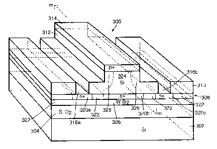
Referring now to Figure 4, an optical device of the invention indicated
generally by
300 comprises in sequence a silicon substrate 302, silicon dioxide layer 304,
a buried
tungsten silicide layer (W Si2) 306, a n+ doped silicon buried contact layer
308 and a
silicon surface layer 310. The layers 302 to 310 are parallel, overlaid and
unitary.
The surface layer 310 is etched to form an exposed rib 312. A reference axis m-
m' is
included in Figure 4 and is orientated in a direction along the rib 312. An
upper
surface of the rib 312 is doped to fiorm an elongate p+ electrode 314. The
electrode
314 and the rib 312 are aligned parallel to one another. The surtace layer 310
is
selectively etched in regions remote from the rib 312 to form two via channels
316a,
316b for making electrical connection to the buried contact layer 308.
Electrical
connection is achieved by depositing doped polysilicon or metal tracks (not
shown)
into the channels 316a, 316b. The layer 308 is selectively doped in regions
320a,
320c near the channels 316a, 316b and in a region 320b near the rib 312,
resulting in
lesser doped regions 322 between the regions 320a, 320b, 320c. The silicide
layer
306 is in a range of 100 nm to 250 nrn thick.
CA 02284197 1999-09-17
WO 98/43128 PCT/GB98/00585
-16-
The p+ electrode 314 is doped with boron to an impurity concentration in- a-
range of
10'8 to 10'9 atoms cm-3. The rib 312 is 4 ~.m wide in a direction orthogonal
to the
axis m-m' and parallel to the surface layer 310. It is 6.5 pm high from the
buried
contact layer 308 in a normal direction therefrom. The surface layer 370 is
3.3 ~m
thick in a direction normal to the buried contact Payer 308 in regions remote
from the
rib 312. The contact layer 308 is 0.1 pm thick and is doped with an electron
donor
impurity to a concentration in a range of 10'8 to 10'9 atoms cm-3. The silicon
dioxide
layer 304 is at least 1 ~m thick for reducing leakage loss of optical
radiation from the
rib 312.
The operation of the device 300 will now be described. The rib 312 forms a
waveguide along which optical radiation of wavelength in a range of 1.3 ~m to
1.5 ~m
propagates, in particular radiation of 1.3 ~m and 1.5 ~m wavelength which is
often
employed in optical communication systems. The radiation is confined within
the
waveguide by a difference in refractive index between the rib 312, the buried
contact
layer 308, the silicide layer 306, the silicon dioxide layer 304 and a low
dielectric
constant medium (not shown) surrounding the device 300.
When a potential difference is applied to bias the p+ electrode 314 at a
higher
potential than the buried contact layer 308, charge carriers are injected
predominantly into a central region 324 of the rib 312. A charge distribution
is
thereby generated where there is a greater concentration of the carriers in
the central
region 324 in which a majority of the optical radiation is confined in
comparison to
edge regions 326 of the rib 312. The carriers injected into the waveguide
thereby
efficiently modulate the radiation in comparison to the prior art modulator
device 1 in
Figure 1. In the device 300, the injected carriers provide phase modulation of
the
radiation within the waveguide. This phase modulation is converted to
amplitude
modulation by inserting the device 300 into one arm of a Mach-Zehnder
interferometer (not shown) in a similar manner to the prior art modulator
device 1.
The tungsten silicide layer 306 has a greater conductivity than the buried
contact
layer 308. It reflects optical radiation efficiently, thereby providing
improved
confinement of radiation within the rib 312. Moreover, the silicide layer 306
also
CA 02284197 1999-09-17
WO 98/43128 PCT/GB98100585
-17-
provides a lower resistance connection to all regions of the contact layer 308
thereby
. enhancing high frequency modulating performance of the device 300 and--
reducing
power dissipation therein. Series resistance of the device 300 may be reduced
by an
order of magnitude compared to prior art devices of equivalent size .
The regions 320a, 320b, 320c in the buried contact layer 308 are formed by
selectively implanting a dopant into the silicide layer 306 and then
subsequently
diffusing the dopant into the buried contact layer 308 after wafer bonding
which will
be described later.
Selectively doping the regions 320a, 320b, 320c provides an advantage that
current
flowing through the via channels 316a, 316b is predominantly diverted into the
silicide
layer 306, and injection of carriers from the region 320b occurs predominantly
into the
central region 324 of the rib 312 thereby improving modulation efficiency of
the
device 300. The layer 306 has a coefficient of resistivity of less than 1.5
~f2m,
namely a sheet resistivity of less than 7.5 S2 per square when the layer 306
is 200 nm
thick. A silicon enriched tungsten silicide film having a composition W Si2,~
has been
experimentally characterised and found to have a coefficient of resistivity of
approximately 0.4 ~S2m which corresponds to a sheet resistivity of
approximately 2 s2
per square for a 200 nm film thickness.
In a simplified version of the device 300, selective doping is not applied to
the regions
320a, 320b, 320c. Instead, the contact layer 308 is substantially uniformly
doped.
As an alternative to fabricating the layer 306 using tungsten silicide, at
least one of
titanium silicide, tantalum silicide and cobalt silicide may be used.
The silicon dioxide layer 304 electrically isolates the silicon substrate 302
from the
silicide layer 306. This provides an advantage of isolating the rib 312 from
the
substrate 302 so that potentials applied to inject charge carriers into the
rib 312 are
not restricted by potential of the substrate 302 as in prior art optical
devices
described earlier.
Another optical device of the invention is indicated by 400 in Figure 5. It
comprises in
sequence a polysiiicon n+ phosphorus doped conduction layer 402, a silicon
dioxide
CA 02284197 1999-09-17
WO 98/43128 PCT/GB98/00585
-18-
insulating buried layer 404 and a silicon surface layer 406. The surface layer
406 is
low doped silicon with an impurity concentration of less than 10'6 atoms cm-3.
It is
etched back to form an exposed rib 408. A reference axis n-n' is included in
Figure 5
and is orientated in a direction along the rib 408. An upper surface of the
rib 408 is
doped with boron impurity to form an elongate p+ electrode 410. The rib 408
and
the p+ electrode 410 are aligned parallel to one another. A central region 411
of the
rib 408 is situated beneath the p+ electrode 410. Via channels 412a, 412b are
remote from the rib 408 and are formed by etching through the surface layer
406 and
the buried layer 404 to the conduction layer 402 to enable electrical
connection to be
made to it. Electrical connection to the conduction layer 402 is achieved by
depositing doped polysilicon or metal tracks into the via channels 412a, 412b.
An
elongate n+ doped electrode region 414 is formed by selectively etching
through the
insulating buried layer 404 and a short distance of 0.5 p.m into the surface
layer 406
to form a channel in which doped polysilicon of the layer 402 is deposited.
The
electrode region 414 is aligned along the axis n-n' and is situated on an
opposite side
of the central region 411 relative to the p+ electrode 410. The rib 408 is a
monomode
waveguide for confinement of optical radiation of wavelength in a range of 1.3
~m
and 1.5 Vim, in particular radiation of 1.3 fcm and 1.5 pm wavelength which is
often
employed in optical communication systems.
The conduction layer 402 and p+ electrode 410 are doped with impurity atoms to
a
concentration in a range of 10'8 to 10'9 atoms cm-3. The rib 408 is identical
in size to
the rib 108 illustrated in Figure 3. The surface layer 406 is 3.3 ~m thick in
regions
remote from the rib 408.
When a potential difference is applied to bias the p+ electrode 410 at a
higher
potential than the electrode region 414, charge carriers are injected into the
central
region 411. The electrode region 414 is truncated widthwise to ensure that
injected
charge carriers are predominantly confined to the region 411 and thereby
efficiently
modulate its refractive index. Because of this confinement, interelectrode
capacitance between the p+ electrode 410 and electrode region 414 is less in
the
device 400 in comparison to intereiectrode capacitance of the modulator device
1 for
achieving an equivalent change in refractive index of the rib 6. This
relatively smaller
intereiectrode capacitance provides an enhanced operating bandwidth for the
device
CA 02284197 1999-09-17
WO 98/43128 PCT/GB98/00585
-19-
400 in Figure 5.
Another optical device of the invention is indicated by 500 in Figure 6. It
comprises in
sequence a silicon substrate 502, a first silicon dioxide insulating buried
layer 504, a
polysilicon n+ phosphorus doped conduction layer 506, a second silicon dioxide
insulating buried layer 508 and a silicon surface layer 510. The surface layer
510 is
low doped silicon with an impurity concentration of less than 10'6 atoms cm-3.
It is
etched back to form an exposed rib 512. A reference axis p-p' is included in
Figure 6
and is orientated in a direction along the rib 512. An upper surface of the
rib 512 is
doped with boron impurity to form an elongate p+ electrode 514 along it. The
rib 512
and the p+ electrode 514 are aligned parallel to one another. A central region
516 of
the rib 512 is situated beneath the p+ electrode 514. Via channels 518a, 518b
are
remote from the rib 512 and are formed by etching through the surface layer
510 and
the second buried layer 508 to the conduction layer 506 to enable electrical
connection to be made to it. Electrical connection to the conduction layer 506
is
achieved by depositing doped poiysilicon or metal tracks (not shown) into the
via
channels 518a, 518b. An elongate n+ doped electrode region 520 is formed by
selectively etching through the second insulating buried layer 508 to form a
channel
in which doped polysilicon of the layer 506 is deposited. The electrode region
520 is
aligned along the axis p-p' and is situated on an opposite side of the central
region
51fi relative to the p+ electrode 514. The rib 512 is a monomode waveguide for
confinement of optical radiation of wavelength in a range of 1.3 ~,m and 1.5
Vim, in
particular radiation of 1.3 pm and 1.5 ~m wavelength which is often employed
in
optical communication systems.
The conduction layer 506 and the~p+ electrode 514 are doped with impurity
atoms to
a concentration in a range of 10'6 to 10'9 atoms cm-3. The rib 512 is
identical in size
to the rib 108 illustrated in Figure 2. The surface layer 510 is 3.3 wm thick
in regions
remote from the rib 512.
When a potential difference is applied to bias the p+ electrode 514 at a
higher
potential than the electrode region 520, charge carriers are injected into the
central
region 516. The electrode region 520 is truncated widthwise to ensure that
injected
charge carriers are predominantly confined to the region 516 and thereby
efficiently
CA 02284197 1999-09-17
WO 98143128 PCT/GB98/00585
-20-
modulate its refractive index. Because of this confinement, interelectrode
capacitance between the p+ electrode 514 and the electrode region 520 is less
in the
device 500 in comparison to interelectrode capacitance of the modulator device
1 for
achieving an equivalent change in refractive index of the rib 6. This
relatively smaller
interelectrode capacitance provides an enhanced operating bandwidth for the
device
500 in Figure 6.
Referring now to Figure 7, there is shown schematically stages in a
microfabrication
process for producing the device 100. A polished low doped silicon wafer 600
containing a dopant impurity to a concentration of less than 10'6 atoms cm-3
is
exposed to ion implantation to form a heavily n+ doped layer 602 on one side
of it.
The layer 602 contains a dopant impurity to a concentration in a range of 10'8
to 10'9
atoms cm-3. A second polished low doped silicon wafer 604 is thermally
oxidised to
form a thick silicon dioxide surface layer 606 on one side of it. Layers 608,
610
correspond to low doped silicon regions of the wafers 600, 604 respectively.
The
layers 602, 606 are then thermally bonded together at a high temperature of
1100 °C
in an atmosphere of wet oxygen and nitrogen such that they fuse together to
form a
wafer couplet indicated by 612. The atmosphere is created by mixing oxygen,
hydrogen and nitrogen gases which spontaneously react at the high temperature
to
form a gaseous mixture of steam, oxygen and nitrogen. The couplet 612 is then
polished to form a thinned wafer couplet indicated by 614 in which the layer
608 is
polished to remove material as indicated by a dashed line 616 to form a
thinned layer
615. Next, the couplet 614 is exposed to ion implantation to form a heavily
doped p+
surface layer 620 with an impurity to a concentration in a range of 10'8 to
10'9 atoms
cm 3, thereby producing a wafer couplet indicated by 618. Standard
microfabrication
lithographic and dry etching processes are then employed to etch the layers
615, 620
to form a rib 624 in a wafer couplet indicated by 622. A dashed line 625
indicates an
amount of material removed during formation of the rib 624. Next, via channels
628a, 628b are formed by using standard lithographic and etching processes,
thereby
producing a wafer couplet indicated by 626. Further processing stages (not
snown~
on the couplet 626 include metal track deposition for electrical connection to
the n+
doped layer 602 and to the p+ surface layer 620 remaining to provide a
completed
optical device.
CA 02284197 1999-09-17
WO 98/43128 PCT/GB98/00585
-21 -
Fabrication csf the device 200 in Figure 3 is similar to the device 100 in-
Figure 2
except that the tungsten silicide layer 202 is deposited prior to bonding
wafers to form
a couplet.
The process shown schematically in Figure 7 is known as "Bond and Etchback
Silicon on insulator" (BESOI). It has not been used in the prior art for
fabrication of
optical devices for modulating radiation.
Referring now to Figure 8, there is shown schematically stages in a
microfabrication
process for producing the devices 200, 300.
Two polished low doped silicon wafers, namely a first wafer 700 and a second
wafer
702, containing a dopant impurity to a concentration of less than 10's atoms
cm-3 are
required for producing the device 200, 300. The second wafer 702 is exposed to
ion
implantation to form a heavily n+ doped layer 706 on one side of it. The layer
706
contains a dopant impurity to a concentration in a range of 10'8 to 10'9 atoms
cm-3.
The wafer 702 thereby becomes the layer 706 adjoined to a low doped layer 704.
A
tungsten silicide layer 708 is then grown by chemical vapour deposition onto
the n+
doped layer 706. Next, a silicon dioxide surface layer 710 is grown onto the
tungsten silicide layer 708 by chemical vapour deposition.
The first wafer 700 and the surface layer 710 are then thermally bonded
together by
holding them in contact for a period of 60 minutes at a high temperature of
1100 °C in
an atmosphere of wet oxygen and nitrogen such that they fuse together to form
a
wafer couplet indicated by 712: The atmosphere is created by mixing oxygen,
hydrogen and nitrogen gases which spontaneously react at the high temperature
to
form a gaseous mixture of steam, oxygen and nitrogen. The couplet 712 is then
polished to form a thinned wafer couplet indicated by 714 in which the first
wafer 700
is polished to remove material as indicated by a dashed line 716 to form a
thinned
layer 715. Next, the couplet 714 is exposed to ion implantation to form a
heavily
doped p+ surface layer 720 with an impurity to a concentration in a range of
10'8 to
10'9 atoms cm-3, thereby producing a wafer couplet indicated by 718. Standard
microfabrication lithographic and dry etching processes are then employed to
etch
CA 02284197 1999-09-17
WO 98/43128 PCT/GB98/00585
-22-
the layers 715, 720 to form a rib 724 in a wafer couplet indicated by 722. A
dashed
line 725 indicates an amount of material removed during formation of-the rib
724.
Next, via channels 728a, 728b are formed by using standard lithographic and
etching
processes, thereby producing a wafer couplet indicated by 726. Further
processing
stages (not shown) on the couplet 726 include metal track deposition for
electrical
connection to the n+ doped layer 706 and to the p+ surface layer 720 remaining
to
provide a completed optical device.
Regions 730 at the via channels 728a, 728b and beneath the rib 724 incorporate
enhanced doping to increase their conductivity and correspond to the regions
204 of
the device 200 and the regions 320a, 320b, 320c of the device 300. They are
formed
by at least one of:
(i) selectively supplementing doping of the n+ doped layer 706 when formed on
the
second water 702; and
(ii) selectively doping the tungsten silicide layer 708 with a dopant and then
arranging
for the dopant to diffuse into the n+ doped layer 706 to selectively dope it.
The process shown schematically in Figure 8 is known as "Bond and Etchback
Silicon on insulator" (BESOI). It is known from prior art that bonds formed
between
silicide layers and silicon layers are highly stressed, hence it would not be
expected
that optical devices employing buried silicide layers could function reliably
or could
even be fabricated. Delamination of bonded silicide layers as a result of
stress is
described in detail on pages 50 to 59 in a book "Silicides for VLSI
Applications" by
S.P. Murarka, Published by Academic Press 1983 ISBN 0-12-511220-3. Buried
silicide layers have not therefore been used in prior art for fabricating
optical devices.
During fabrication of the devices 200, 300 illustrated in Figures 3 and 4, it
has been
found that bonding of the tungsten sificide layer 708 to the n+ doped layer
706 and
the silicon dioxide layer 710 is enhanced by adjusting stochiometric
composition of
the silicide layer 708 so that it is silicon enriched. Moreover, it has been
found that
bonding stresses between the silicide layer 708 to the n+ doped layer 706 and
the
silicon dioxide layer 710 may be reduced by selectively etching regions of the
silicide
layer 708, namely patterning it before growing the silicon dioxide layer 710
onto it.
Such patterning may include regularly spaced isolation channels or holes,
namely
voids, where the silicide layer 708 has been selectively etched or eroded, for
example
CA 02284197 1999-09-17
WO 98/43128 PCT/GB98/00585
-23-
using ion milling, away. Alternatively, the silicide layer 708 may be
patterned so that
- it is incorporated as isolated islands of silicide.
Referring now to Figure 9, there is shown schematically stages of a
microfabrication
process for producing the device 400 in Figure 5. A low doped silicon wafer
850
containing a dopant impurity of concentration less than 10'6 atoms cm-3 is
exposed to
phosphorus dopant implantation to form a wafer indicated by 852 incorporating
an
implanted n+ surface layer 854 on it. The layer 854 contains dopant to a
concentration in a range of 10'8 to 10'9 atoms cm-3. A low doped silicon wafer
856 is
oxidised to form a 1 um thick surface silicon dioxide layer 858 onto it. A
channel 860
is etched into the silicon dioxide layer 858 by employing standard
microfabrication
lithography and dry etching techniques. A doped polysilicon n+ layer 862 is
then
deposited onto the silicon dioxide layer 858 and into the channel 860. An
exposed
external surface of the layer 862 is then polished to planarise it to form a
wafer
indicated by 864. The wafers 852, 864 are abutted with the surface layer 854
contacting the polysilicon n+ layer 862 and then thermally bonded at a high
temperature of 1100 °C in an atmosphere of wet oxygen and nitrogen to
form a wafer
couplet indicated by 866. The atmosphere is created by mixing oxygen, hydrogen
and nitrogen gases which spontaneously react at the high temperature to form a
gaseous mixture of steam, oxygen and nitrogen. The couplet 866 is polished to
thin
the wafer 856 contained therein to form a layer 868 where a dashed line 870
indicates a quantity of material removed by polishing to form a couplet
indicated by
872. The layer 868 of the couplet 872 is exposed to boron impurity
implantation to
form a doped p+ surface layer 874 to provide a wafer couplet indicated by 876.
The
layer 868 is doped with boron impurity to a concentration in a range of 10'8
to 10'9
atoms cm-3. By employing standard lithographic and dry etching techniques, the
surface layer 874 and the layer 868 are etched back as indicated by a dashed
line
878 except in an area to form a rib 880, thereby providing a wafer couplet
indicated
by 882. Two connection via channels 884a, 884b are then delineated and etched
through the layers 858, 868 to provide a couplet indicated by 886. Further
processing stages (not shown} on the couplet 886 include metal track
deposition for
electrical connection to the n+ layer 862 and to the p+ surface layer 874
remaining to
provide a completed optical device.
CA 02284197 1999-09-17
WO 98/43128 PCT/GB98/00585
-24-
Referring now to Figure 10, there is shown schematically stages of a
microf~brication
process for producing the device 500. Two low doped silicon wafers, namely a
first
wafer 950 and a second wafer 952, containing a dopant impurity of
concentration less
than 10'6 atoms cm-3 are oxidised to form 1 um thick silicon dioxide surface
layers
954, 956 onto them respectively to form wafers indicated by 958, 959
respectively. A
channel 960 is then etched into the silicon dioxide layer 956 by employing
standard
microfabrication lithography and dry etching techniques. A doped polysilicon
n+ layer
962 is then deposited onto the silicon dioxide layer 956 and into the channel
960. An
exposed external surface of the layer 962 is then polished to planarise it to
form a
wafer indicated by 964. The wafers 958, 964 are abutted with the surface layer
954
contacting the polysilicon n+ layer 962 and then, whilst being maintained in
contact,
thermally bonded at a high temperature of 1100 °C for a period of 60
minutes in an
atmosphere of wet oxygen and nitrogen to form a wafer couplet indicated by
966.
The atmosphere is created by mixing oxygen, hydrogen and nitrogen gases which
spontaneously react at the high temperature to form a gaseous mixture of
steam,
oxygen and nitrogen. The couplet 966 is polished to thin the wafer 952
contained
therein to form a layer 968 where a dashed line 970 indicates a quantity of
material
removed by polishing to form a couplet indicated by 972. The layer 968 of the
couplet 972 is exposed to boron impurity implantation to form a doped p+
surface
layer 974 to provide a wafer couplet indicated by 976. The layer 968 is doped
with
boron impurity to a concentration in a range of 10'8 to 10'9 atoms cm-3. By
employing standard lithographic and dry etching techniques, the surface layer
974
and the layer 968 are selectively etched back as indicated by a dashed line
978
except in an area to form a rib 980, thereby providing a wafer couplet
indicated by
982. Two connection via channels 984a, 984b are then delineated and etched
through the layers 956, 968 to provide a couplet indicated by 986. Further
processing stages (not shown) on the couplet 986 include metal track
deposition for
electrical connection to the n+ layer 962 and to the p+ surface layer 974
remaining to
provide a completed optical device.
In Figure 10, a bonding interface is provided between the doped polysilicon n+
layer
962 and the silicon dioxide surface layer 954. In an alternative
microfabrication
process for fabricating the device 500, the surface layer 954 may be deposited
onto
CA 02284197 1999-09-17
WO 98/43128 PCT/GB98/00585
-25-
the n+ layer 962 instead of onto the first wafer 950 so that a bonding
interface is
provided between the surface layer 954 and the first wafer 950. - -
It is not feasible to fabricate the devices 200, 300, 400, 500 illustrated in
Figures 3 to
6 using epitaxial techniques. The tungsten silicide layer 202, 306, the
polysilicon
layer 402, 506 and the silicon dioxide layer 304, 504 are not monocrystalline.
As a
consequence of this, any layer grown epitaxially onto any of said layers 202,
304,
306, 402, 504, 506 will also not be monocrystailine. Thus, with said layers
present, it
is not feasible to grow epitaxially onto them monocrystalline layers suitable
for
fabricating the rib 108, 314, 408, 512. Hence, the processes illustrated in
Figures 7
to 10 are essential for fabricating the devices 200, 300, 400, 500.
Referring now to Figures 2 to 6, the ribs 108, 312, 408, 512 may be gold doped
in
order to increase device operating bandwidth by ensuring rapid removal of
charge
carriers by recombination. As an alternative to gold doping, charge carrier
recombination within the ribs 108, 312, 408, 512 may be increased by forming
lattice
defects therein which function as recombination sites. Such defects may be
introduced by exposing the ribs 108, 312, 408, 512 to high power laser,
electron or
hydrogen ion beams. Alternatively, the ribs 108, 312, 408, 512 may be exposed
to
intense neutron beams for introducing the defects.
In Figures 2 to 6, dopant types may be swapped, namely n+ doped and p+ doped
regions become p+ doped regions and n+ regions respectively, to provide
alternative
optical devices of the invention. This does not affect their mode of operation
other
than reversing polarity of applied potential required for injecting charge
carriers into
the rib 108, 312, 408, 512. Although thermal bonding of wafers at a
temperature of
1100 °C is described above, satisfactory bonding may be achieved in a
range of
temperatures from 800 °C to 1200 °C. Although provision of the
atmosphere of wet
oxygen and nitrogen described above may improve bonding strength, it is not
essential for achieving a thermal bond between wafers. The bond is
sufficiently
robust to survive further high temperature processing steps, for example steps
necessary for integrating electronic circuits onto the wafers. Other methods
of
bonding may also be used to fabricate the device instead of employing thermal
bonding, for example fusion bonding.
CA 02284197 1999-09-17
WO 98!43128 PCT/GB98/00585
-26-
Electronic circuits may be monolithically integrated with the devices 100,
X00, 300,
400, 500. These circuits may comprise, for example, buffer amplifiers and
logic
gates. The circuits may be fabricated after formation of the rib 108, 312,
408, 512,
624, 724, 880, 980. Alternatively, the circuits may be formed prior to
formation of the
rib 108, 312, 408, 512, 624, 724, 880, 980 and may be protected from etching
in a
similar manner to which the rib itself is protected during etching, for
example by a
resist layer or a metallic masking layer which is later removed by processes
such as
sputtering, plasma etching or wet chemical etching.
Although the rib 108, 312, 408, 512, 624, 724, 880, 980 incorporates dopant
impurity
to a concentration of less than 10'6 atoms cm-3, the concentration may be
increased
above 10's atoms cm-3 with a consequence that radiation absorption within the
device 100, 200, 300, 400, 500 increases correspondingly,
Although the optical devices 100, 200, 300, 400, 500 shown in Figures 2 to 6
are
based on silicon semiconductor technology, they may alternatively be
fabricating
using wafer bonding techniques in Ill-V semiconductor materials.
Although fabrication of single optical devices is illustrated in Figures 7 to
10, it is
possible to fabricate a number of devices simultaneously on the wafers 600,
604,
700, 702, 850, 856, 950, 952. The devices thereby fabricated may be separated
from one another by dicing or sawing the couplets 626, 726, 886, 986, said
devices
then comprising elements of the wafers 600, 604, 700, 702, 850, 856, 950, 952
which
are bonded together. Alternatively an array of the devices 100, 200, 300, 400,
500
may be fabricated on a wafer couplet for providing a phased array device.
Although the devices 100, 200, 300, 400, 500 are adapted to modulate
radiation, use
of high conductivity buried layers, for example metal silicide layers, in
other types of
semiconductor optical devices, for example high power solid state lasers, is
also
feasible for providing an electrical path of reduced series resistance for
applying bias
to said devices.