Note : Les descriptions sont présentées dans la langue officielle dans laquelle elles ont été soumises.
CA 02284311 1999-09-29
1
SWITCH ARCHITECTURE FOR DIGITAL MULTIPLEXED SIGNALS
FIELD OF THE INVENTION
The invention relates to switches and, more particularly, to multi-channel,
non-blocking switches.
BACKGROUND OF THE INVENTION
Switches are employed in a wide variety of communications systems to
route digital signals, such as voice, data, video, and audio signals, from one
or
more sources to one or more destinations. An NXM multi-port switch may be used
to connect any of N input data channels to any of M output data channels. Each
of the data channels may be assigned its own physical channel or multiple
channels may be multiplexed onto a single physical channel in order to share
the
physical channel. A strictly non-blocking switch guarantees a connection path
will
be available between each input channel and each output channel without
rearrangement of any existing connections among other ports. A crossbar switch
~5 is one example of a strictly non-blocking switch. Some applications,
notably
synchronous optical network (SONET) systems, require switches to provide, in
addition to permutation capability exemplified by non-blocking performance,
multi-
cast or broadcast capability. That is, switches must feature the ability to
switch
data from any of the switch's input channels to several or all of its output
channels.
2o Providing non-blocking switching capability for large numbers of
synchronous
transport signals such as level one (STS-1 ), level three (STS-3), level
twelve
(STS-12), or other channels within a SONET system can be particularly
challenging. SONET and STS-1 are known and discussed, for example, in U.S.
Patent 5, 715,248 issued to Lagle et al, U.S. patent 5,781,320 issued to
Byers,
25 U.S. Patent 5,742,605 issued to Norman, U.S. patent 5,383,196 issued to
Morton, and U.S. Patent 5,682,257 issued to Uchida, all of which are hereby
incorporated by reference.
CA 02284311 1999-09-29
2
The number of physical channels (e.g., optical fibers, twisted wire pairs, or
coaxial cables) required to carry a group of data channels is often minimized
by
multiplexing data channels onto a single physical channel, thus avoiding the
capital expense associated with installing and maintaining additional physical
s channels. One consequqnce of such signal consolidation is the multiplication
of
data rates on the physical channel. When such high data rate signals are to be
switched, the multiplexed data channels may be demultiplexed in order to
accommodate the switching speed limitations of the device that is to
physically
switch data from an input channel to an output channel. For example, a ten-
~o channel, one gigabit per second (Gbs) physical channel could be
demultiplexed
to ten 100 megabit per second (Mbs) data channels, thereby significantly
reducing
the switching speed requirements imposed upon the physical switch. There is,
therefore, a tradeoff between the number of data channels that may be
consolidated on a physical channel and the operating speed required of devices
~ s that switch the data channels. Additionally, restrictions on the number of
physical
inputloutput connections available to a switch tend to force the consolidation
of
data channels onto a limited number of physical channels. Restrictions due to
input/output limitations are particularly evident at the integrated circuit
package
level, where designs are sometimes pinout limited. That is, although the
specific
2o desired circuit may physically fit within the integrated circuit's (IC's)
size
limitations, there are not enough inputloutput pins available accommodate all
the
signals that must be brought into or taken off of the circuit. Or, the
inputloutput
buffers required for that number of inputs and outputs may dissipate too much
power. Additionally, the interconnection of various circuit elements on an IC,
the
25 interconnection's routing, presents greater difficulties as the complexity
of the
integrated circuit increases and there tends to be a tradeoff between pinout
and
size limitations.
In addition to the well known advantages of modular design, such as the
reduction of design effort, the re-use of standardized, fully-tested, and
therefore
3o reliable modular building blocks, and economies of scale associated with
the
CA 02284311 1999-09-29
3
production of large numbers of modules, modular designs may permit a designer
to balance the competing demands of inputloutput, device size, signal speed,
and
routing limitations.
A modular switch that accommodates inputloutput limitations, device
s switching speed limitatioris, routing, and device size limitations would
therefore be
highly desirable.
SUMMARY OF THE INVENTION
In a switch in accordance with the principles of the present invention,
switch modules, each of which includes a disassembly block, a switching core,
~ o and an assembly block, are combined to implement an NXM multi-port switch
that
effectively connects N input ports to M output ports and provides broadcast
capability. Such switches may also be implemented as non-blocking switches.
In an illustrative embodiment, each switch module includes physical
channels, referred to as input and output ports, each of which carries at
least one
~5 input or output data channel. All the data channels have their respective
data
blocks organized in the same number of bit-packs. For example, if the data
channels to be switched contain data organized in bytes, i.e., each data block
is
eight bits long, and the bit-packs (that are fractions of data blocks) are
organized
as single bits, i.e., each bit-pack is one bit long, eight modules, one for
each bit-
2o pack, will be combined to form a switch. Similarly, a thirty-two bit data
block may
be organized as thirty-two one-bit bit-packs, eight four-bit bit-packs, four
eight-bit
bit-packs, etc., with thirty two, eight or four modules, respectively employed
to
switch the data channels. Although data blocks may be organized as any number
of bit packs and bit packs may be organized as any number of bits, for the
ease
25 of description, unless otherwise indicated, the following discussion will
generally
assume that a data block contains eight bits and a bit pack contains one bit.
A disassembler within each module disassembles, or "slices", the data
blocks it receives into bit-packs, routing bit-packs from the channels to
switching
CA 02284311 1999-09-29
~ 4
cores. For example, in a module that receives byte wide data blocks and
operates
on one-bit bit-packs, the disassembler slices each byte into eight bits and
routes
each of the bits to a different one of the switching cores within the eight
switch
modules that comprise such a switch.
s A switching core wii'hin each module connects each input channel with each
output channel at the bit-pack level. That is, each switching core is assigned
a
specific bit-pack upon which to operate, receives those bit-packs for all the
channels and routes those specific bit-packs to the appropriate assembler,
and,
through the assembler, to an output channel. For example, in a switch that
0 operates upon channels having byte-wide data blocks and switches at the bit
level
(one-bit bit-packs), one switching core will receive and switch the first bit
of each
byte from all the input channels, a second switching core will receive and
switch
the second bit from all the input channels, a third switching core will
receive and
switch the third bit from all the input channels, etc.
~s Assemblers within each module receive the switched bit-packs from each
switching core and assemble the bit-packs into data blocks for each of the
output
channels
BRIEF DESCRIPTION OF THE DRAWINGS
The above and further features, aspects, and advantages of the invention
2o will be apparent to those skilled in the art from the following detailed
description,
taken together with the accompanying drawings in which:
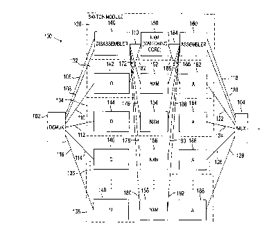
Figure 1 is a conceptual block diagram of an N X M switch in accordance
with the principles of the present invention;
Figure 2 is a functional level block diagram of a switching module in
2s accordance with the principles of the present invention;
Figure 3 is a functional level block diagram of a 2 X 2 switch that employs
the switching modules in accordance with the principles of the present
invention;
CA 02284311 1999-09-29
Figure 4 is a functional level block diagram of a space/time switching core
in accordance with the principles of the present invention;
Figure 5 is a functional level block diagram that depicts a combination of
switching modules that comprise 768 X 768 non-blocking SONET switch;
s Figure 6 is a bit map that illustrates one possible organization of 768
channels for switching by a 768 X 768 switch such as the switch of Figure 5;
Figure 7 is a functional level block diagram of a switching core in
accordance with the principles of the present invention;
Figure 8 is a functional level block diagram of an alternative embodiment
~o of a switching core in accordance with the principles of the present
invention;
Figure 9 is a block diagram of a switching module in accordance with the
principles of the present invention which depicts the interconnection paths
for one
switching module of an eight-module switch;
Figures 10A and 10B are, respectively, input and output maps of a
~s switching core in accordance with the principles of the present invention;
Figures 11A and 11 B are, respectively, a block diagram representation of
a 96 X 96 SONET switch that employs only one switching module, and the
corresponding inputloutput matrix;
Figure 12 is a functional level block diagram of an eight-module 576 X 576
2o SONET switch;
Figures 13 A and 13B are, respectively, a functional level block diagram of
a multi-bit switching module, and a 768 X 768 SONET switch employing four of
such modules;
CA 02284311 1999-09-29
- 6
Figures 14A and 14B are, respectively, a functional level block diagram of
a multi-bit switching module and a 576 X 576 switch employing four of such
modules.
DETAILED DESCRIPTION
i
s Although data blocks may be organized as any number of bit packs and bit
packs may be organized as any number of bits, for the ease of description,
unless
otherwise indicated, the following examples will generally assume that a data
block contains eight bits and a bit pack contains one bit. The conceptual
block
diagram of Figure 1 illustrates the basic organization of a strictly non-
blocking N
o by M switch in accordance with the principles of the present invention. A
switch
100 accepts data from an optional dernultiplexer 102 and switches the data
from
each of the N input data channels to selected M output data channels. After
switching, the output channels are routed to an optional multiplexer for
concentration into a fewer number of physical channels. The switch includes N
1 s input data ports, 106-116 and M output data ports 118-128. The data ports
106-
128 provide physical channels between the switch 100 and other devices, such
as the demultiplexer 102 and multiplexer 104 of the illustrative embodiment.
In the
illustrative embodiment, each data channel is assigned its own data port. The
data within each data channel is organized in data blocks composed of bit-
packs.
2o All data channels may have data organized as byte-wide data blocks composed
of 1 bit, bit-packs, for example. The switch includes O switch modules 130-
138,
where O is the number of bit-packs in a data block. For example, O = 8 when
data
blocks are 1 byte wide and bit-packs are 1 bit-wide, 0 = 4 when data blocks
are
1 byte-wide and bit-packs are 2 bits wide, and so on.
2s The O switch modules 130-138 each include at least 1 input port and 1
output
port. In the illustrative embodiment, all switch modules have the same number
of
input ports and the same number of output ports. Some of these ports are
omitted
from Figure 1 for clarity. The switch module 130 includes input ports 106 and
108
and output ports 118 and 120 and provide two physical channels each for input
CA 02284311 1999-09-29
7
data channels to and output channels from the switch module 130. Each of the
switch modules 130-138 includes a disassembler 140-148, which accepts data
from the associated input ports, a switching core 150-158 which accepts and
switches bit-packs from each of the disassemblers, and an assembler 160-168
s which accepts switched lit-packs from each of the switching cores. Each of
the
switch module components will be described in greater detail below.
In accordance with the principles of the illustrative embodiment, when the
switch module 130 receives a data block, e.g. a byte, the disassembler 140
slices
the data block into bit-packs, e.g. bits, and distributes the bits to the
various
switching cores 150-158. Consequently, all the respective bit ones, twos,
threes,
fours, fives, six, sevens, and Bights from data channels input to the
disassembler
140 are respectively routed to the switching core 150, 152, 154, 156, . . .
158.
The respective connection paths 170, 172, 176, 178, and 180 from disassembler
140 to switching cores 150-158 are illustrated in Figure 1. A connection path
182,
~5 which provides a route for all bit ones from disassembler 142 to the
switching core
150 is also illustrated. The remaining connection paths between the
disassembler
and switching cores have been eliminated from Figure 1 for clarity. Similarly,
the
respective connection paths 184, 186, 188, 190, and 192 which carry the
switched
bits 1-8 for the assembler 160 are shown. A connection path 194 from switching
2o core 150 carries a switched bit 1 from the switching core 150 to the
assembler 162
which assembles switched bits 1-8 from respective switching cores 150-158.
Switching cores 150-158 are connected to assemblers 160-168 and, in a similar
fashion, several of the connection paths are omitted from Figure 1 for
clarity.
In operation, data from data channels is routed to the disassemblers 140-148
2s which bitwise slice the data (assuming one bit bit-packs) and send the
sliced data
to the switching cores 150-158, each of which switches all the respective bit
data
from all the input channels and distributes the switched bit data to the
appropriate
assemblers 160-168 for assembling into data blocks for the output ports 118-
128.
CA 02284311 1999-09-29
8
- The block diagram of Figure 2 provides a more detail view of a switch
module,
such as switch module 130 of Figure 1, with like components having like
designation numbers. Each switch module 130 may include N input ports 106,
108, . . . 109, and M output ports 118, 120, . . . 121. For example, in an
illustrative
s embodiment where each data block is 8 bits wide, each bit-pack is one bit
wide,
and 768 input data channels are switched onto 768 output data channels, the
number of input ports and output ports on each switch module would be 768 = 8
= 96 input ports and 96 output ports. Data from each of these input ports is
disassembled in the disassembler 140 and the disassembled bit-packs, e.g.
single
o bits in a one bit bit-pack implementation, are distributed along the
connections
170, 172, . . . 173, to an internal switching core 150, and switching cores of
other
switch modules (not shown). If only one data channel is disassembled within
each
disassembler, each of the connections 170, 172, 173, carries bit-pack data for
only one data channel. On the other hand, if a plurality of data channels are
1 s accommodated by each switch module, each of the connection paths 170-173
may
include bit-pack data from a plurality of data channels. The number of
connection
paths leading from the disassembler 140 to other switch modules is equal to
the
number of switch modules 0-1, but each of the connection paths may carry a
plurality of data channels. Additionally, each connection path may include a
2o plurality of physical paths, such as wires, printed circuit traces, or
conduction
paths in an integrated circuit. The number of switch modules is determined by
the
number of bit-packs in a data block, e.g. 8 bits in a byte.
Similarly, a total of O -1 connection paths 182 -183 link other disassemblers
to the switching core 150, O -1, 194-195 connections link the switching core
150
25 to other assemblers, and O -1, 186-187 connection paths link other
switching
cores to the assembler 160. Each of these connection paths may transmit bit-
packs from a plurality of data channels so that, for example, 8 connection
paths
170, 182, . . . 183 may each carry bit-pack data from 96 data channels,
thereby
providing data for 768 data channels to the switching core 150. The
disassembler
ao 140 and assembler 160 may respectively include a demultiplexer and a
CA 02284311 1999-09-29
_ 9
multiplexer. With multiplexer and demultiplexer included in this example, the
96
input channels to the disassembler 140 may be carried on 8 physical channels,
for example.
The functional level block diagram of Figure 3 illustrates the structure of a
2
s channel, 2-bit data block, 1-bit, bit-pack switch 300 in accordance with the
principles of the present invention. The switch 300 includes switch modules
302
and 304. As previously described, each switch module 302 and 304 respectively
includes disassemblers 306 and 308, switching cores 310 and 312, and assembler
314 and 316. A demultiplexer 318 receives input data channels ch1 and ch2 and
~o demultiplexes the data, sending ch1 data to the switch module 302 and ch2
data
to the switch module 304. The disassembler 306 disassembles each 2-bit data
block into 1-bit bit-packs and respectively routes channel 1, bit-1 (c1 b1 )
and
channel 1, bit-2 (c1 b2) to switching cores 310 and 312. Similarly, the
disassembler 308 disassembles each 2-bit data block of channel 2 and
~s respectively routes channel 2, bit-1 (c2b1) and channel, bit-2 (c2b2) to
switching
cores 310 and 312.
The switching cores 310 and 312 respectively switch bit-1 data from channels
1 and 2 to outgoing channels 3 and 4. Consequently, the switching core 310
routes channel 3, bit-1 (c3b1 ) and channel 4, bit-1 (c4b1 ) data to
assemblers 314
2o and 316, respectively. Similarly, the switching core 312 routes channel 3,
bit-2
(c3b2) and channel 4, bit-2 (c4b2) data to assemblers 314 and 316,
respectively.
Assemblers 314 and 316 respectively assemble the channel 3 and channel 4 bit-
packs into 2-bit data blocks which are transferred to the multiplexer 320. The
multiplexer 320 multiplexes data blocks from channels 3 and 4 and produces an
2s output data stream ch3/ch4.
A conceptual block diagram of a 4 X 4 switching core 400 in accordance with
the principles of the present invention is illustrated in Figure 4. The switch
400 is
a spaceltime switch in that it combines physical, or space, switching with
time
switching in order to accommodate the competing demands of signal speed and
CA 02284311 1999-09-29
- 10
switch size limitations. That is, a switch may be made physically smaller if
bit-
packs can be switched sequentially, using time switching. At the same time,
high
speed signals can be switched when the switching takes place in parallel,
using
space switching. As will be apparent from the examples to follow, one factor
may
s be traded off against the ether to obtain an appropriate mix of size and
speed for
a given implementation.
In this illustrative embodiment, the first bits of 4 input channels, c1 b1
through
c4b1 are switched to the first bits of 4 output channels, c5b1 through c8b1. A
4
to 2 multiplexes 402, multiplexes bit-pack, first bits routed to the switching
core
400 from various disassemblers, to 2 to 1 multiplexers 404, 406, 408, and 410.
In this illustrative embodiment, during the first time slot, the multiplexes
402
selects bits c1 b1 and c2b1 and routes those bits to 2 to 1 multiplexers 404-
410.
During the second time slot, the multiplexes 402 selects bits c3b1 and c4b1
and
routes them to the 2 to 1 multiplexers 404-410. In this manner, each of the 2
tc
~s 1 multiplexers 404-410 may select any input, c1b1 through c4b1 to latch
into a
storage area 412-418, respectively. The storage areas 412-418 are often
depicted, and will be hereinafter, as a switch matrix that may correspond to a
combination of time slots and physical connection paths referred to as rails.
Instead of switching bits in two time slots, as in this illustrative
embodiment, all bits
2o could be switched in a single time slot by replicating a 4 to 1 multiplexes
for each
output bit location 412-418. However, such an embodiment might require higher
speed circuitry and may consume more space. If the space and high-speed
circuitry are available, such a switch may be incorporated as a switching core
within a switch module in accordance with the principles of the present
invention.
2s As will be apparent from the following examples, different scales, e.g.,
much
larger switches, and different levels of multiplexing are contemplated within
the
scope of the invention.
The new, modular, non-blocking switch is particularly suited to complex
applications, such as the non-blocking switching of 768 X 768 STS-1 channels
CA 02284311 1999-09-29
' 11
within a SONET system. In the illustrative embodiment of Figure 5, where like
elements have like reference numbers, the modular switch accommodates board
pin, device pin, device-size and power dissipation limitations by employing a
bit-
slice approach (e.g., each bit-pack is one bit wide). In this illustrative
embodiment
the switch includes eight;switch modules, with one switching core for each
bit.
Each disassembler within each switch module disassembles data from 96 STS-1
channels, distributing the data bits from all the channels to the appropriate
switching core. For example, all first bits from all 768 channels may be
routed to
the first module's switching core 150 for switching, second bits from all 768
o channels may be routed to the second module's switching core 152 for
switching.
etc.
In the following example it is assumed that all the 768 STS-1 signals are
synchronized to a single clock in a stage prior to the switch comprising the
eight
switch modules. Although, in the illustrative embodiment, the modular switch
~s operates on bit sliced data that is sliced one bit wide, that is, one bit
bit-packs are
employed, the same considerations would apply to a device which operates on 2
bit bit-packs.
Within each switching core 150-158 all the relevant bits (e.g., bit 1's for
switch module 130, bit 2's for switch module132, etc.) are illustratively
input to
2o the switching core on 16 rails in 48 time slots (note that 16x48=768). Each
rail
is carrying data at the rate of 311.04 Mbls. In this manner, the data rate of
768
STS-1 signals can be accommodated by 8 such devices. That is, since the
transmission rate of an STS-1 signal is 51.84 megabits per second (Mbps), 768
such signals would yield a transmission rate of 39.81 Gigabits per second
2s (Gbps). Because each device's switching core operates on one bit of each of
the 768 channels in parallel, with each bit being processed at a rate of
(number of rails per switching core) X (number of switching cores)X( switch
processing speed) = 16 X 8 X 311.04 Mbps = 39.81 Gbps, the data rate of 768
STS-1 signals. Internal to each switching core, the data may be demultiplexed
CA 02284311 1999-09-29
12
onto 32 rails operating at half the rate: 155.52 Mbls. In that case, the 768
bits
would be available over 32 rails in 24 time slots (note 32x24=768). Such
demultiplexing can be continued further where data is carried over twice as
many rails, each operating at half the rate.
s The input data bits of the illustrative embodiment can be represented by a
matrix such as shown in figure 6, in which each row represents a rail and each
column represents a time slot. Each incoming STS-1 signal's data bit may be
placed by a rail number and a slot number. Such a matrix will be referred to
hereinafter as an input bit map. Similarly, the switches output may be
represented
by an output bit map in which each outgoing STS-1 channel is identified by G;
outgoing rail number and time slot number.
The switch operates under the control of a switch control map which
specifies the source, which may be an STS-1 number or the incoming rail and
slot
number in the matrix representation of Figure 6 for each of the 768 bits in
the
~s output bit map. Assuming that the data rails have been demultiplexed as
indicated
above and are represented by the matrix of Figure 6, the row numbers would
span
the range of 1-32 and time slot numbers span the range of 1-24. Thus, a 10 bit
number corresponding to each output bit can represent the source for the
outpu4
bit and consequently, the switch control map could be implemented by storing
20 7680 bits. If, for example, the switch control map contains rail 2, slot 21
in all 768
entries, input bits from rail 2 slot 21 would be broadcast to all the output
channels.
If all the 768 entries in the switch control map are unique, that would
correspor~~
to a permutation network because each of the output bits are being sourced
from
a different location. The switch may accommodate any combination of mixture of
2s broadcast and permutation.
Each of the switching cores 150-158 could be implemented as a single
stage space switch. In this case, the incoming bits would be stored for 24
time
slots in order to make all the 768 bits available for switching. Once all the
bits
were available, a 768x768 crossbar switch would then be operated to assemble
CA 02284311 1999-09-29
13
the output bit map. The bits in the output bit map are then sent out on the 32
rails
during the next 24 time slots while the input bit map storage is being filled
with
new data. This requires the equivalent of 768x768 = 589824 crosspoints.
As noted above, the switching cores may be implemented using a
s spaceltime switching architecture in order to reduce the size of the
switching
cores. For example, Instead of operating the crossbar switch only once every
24
time slots (i.e., once every 24x6.43ns = 154.32ns) the switch could be
operated,
or reconfigured, in every time slot. This would permit a twenty four-to-one
reduction in the size of the switching cores. In the illustrative 768 X 768
~o embodiment, each such time-multiplexed switching core would be roughly
equivalent in size to a purely space switch having 768x768124 = 24576
equivalent
crosspoints. The time-multiplexed, or space/time, implementation would include
additional timing and control complexities, but may offer other advantages.
Such spaceltime switches may be implemented in a variety of
~s configurations, with different combinations of rails and time slots. Figure
7
provides a conceptual block diagram of an illustrative embodiment of such
space/time implementation 700, which will be referred to hereinafter as an
expander space/time switch. Such a configuration employs a selection block 701
for each of the seven hundred and sixty eight locations in the switch core's
output
2o bit map. In the illustrative embodiment, each selection block 701 employs a
32 to
one multiplexes 702 to select one of 32 rails. The selected rail may remain
the
same in all 24 time slots 704 because control circuitry, illustrated at the
functions:
level as a combination of an "exclusive or" gate 708 and latch 710, is
associated
with each of the seven hundred and sixty-eight multiplexers 702 and serves to
2s latch into the output bit map 706 the desired bit of the seven hundred
sixty eight
bits input to the multiplexes over the course of twenty four time slots. That
is, each
32 to 1 multiplexes selects one of 32 rails and the latching action of the
control
circuitry (that is, gate 708 and latch 710) selects the desired time slot of
the 24
time slots. Consequently, the appropriate bit of 768 input bits, one of 32 in
any
CA 02284311 1999-09-29
14
one of the twenty four time-slots, may be selected for writing into a location
within
an output bit map 706.
Since all seven hundred sixty eight input bits, one bit from each input
channel, are sent to each of the selection blocks 701, any one bit may be sent
to
s all the locations within the output bit map 706. That is, the switching core
700 may
be used to broadcast data from any input channel to all the output channels.
For
example, if the selection block 701 points to rail 1, slot 1 in the output bit
map 706
and its source, determined by a switch control map as previously discussed, is
rail
8, slot 19 of an input bit map (not shown), the five bit control input to the
multiplexer 702 could select rail 8 to appear at the output of the multiplexer
70
during all twenty four time slots. The enable circuit, functionally
represented by
the exclusive or circuit 708, would then activate the latch 710 only during
incoming
slot 19, thus selecting the bit appearing on rail 8 in time slot 19 for output
to rail
1 time slot 1. In this illustrative embodiment, after 24 time slots, all the
input bits
~ s have been switched to the appropriate location within the output bit map
706. The
output bit map 706 may then be parallel-loaded into another bitmap 712, which
operates to buffer the output data and to allow the bitmap 706 to be loaded
with
output data for the next successive twenty four time slots.
The regularity of the seven hundred and sixty eight selection blocks 701 can
2o be exploited to organize them into small, efficiently laid-out cells that
are used
repeatedly in an integrated circuit implementation. That is, each of the eight
switching cores employed in this illustrative embodiment may be implemented in
a variety of integrated circuit implementations, whether all eight modules are
packaged within a single integrated circuit, a single integrated circuit
contains a
2s single module, or each module is distributed throughout a plurality of
integrated
circuits. Regardless of packaging, each of the switching cores could be
organized
in any one of a number of efficient layouts.
An alternative switching core 800 is illustrated in the functional level block
diagram of Figure 8. This illustrative embodiment of the switching core
employs
CA 02284311 1999-09-29
thirty-two 768:1 multiplexers 802. In this embodiment an input bit map 804 is
loaded from a 32 bit bus 805 (one rail per bit) in one step far each of twenty
four
time slots. Once the input bit map 804 is thus filled with one bit from each
of
seven hundred and sixty eight channels, the contents are shifted in parallel
to a
5 duplicate input bit map 8Q6. Each of the thirty-two multiplexers 802
transfers a
selected bit to a thirty-two bit output data bus 808 during each of 24 time
slots.
That is, in any time slot, data for the outgoing data bus 808 is generated by
the
32 multiplexers. Each multiplexer 802 has access to all the 768 input map bits
and is dedicated to generating one rail of the output bus. The 10 bit control
input
o to each multiplexer will typically change in during each time slot.
Therefore, In
each time slot no more than 320 control bits of the 7680 bits needed for the
switch
control map are active, and the switch control map could be implemented, for
example, in area-efficient dual port RAM. In the illustrative SONET
application the
multiplexers 802 must operate at 155 Mbs or other steps must be taken to
~s accommodate the SONET data rate. For example, a retiming stage could be
added, with corresponding changes in the timing of the multiplexer control
bits.
The functional level block diagram of Figure 9 provides a more detailed
view of the interconnection paths of one of eight switch modules employed in a
786 X 768 non-blocking SONET STS-1 switch. The switch module 800 includes
2o a disassembler 802, a 768 X 768 single bit switching core 804, and an
assembler
806, all of which are implemented in accordance with the principles of the
present
invention as previously described in the discussions related to disassemblers,
switching cores, and assemblers. In this illustrative embodiment, each switch
module is implemented on a separate integrated circuit and each disassembler
2s and assembler respectively include a demultiplexer and multiplexer.
Each module 800 receives eight STS-12 inputs at the disassembler 802
and provides eight STS-12 outputs at the assembler 806. Since each STS-12
signal consists of 12 STS-1 multiplexed signals, the 8 inputs contain an
equivalent
of 8 x 12 = 96 STS-1 signals. A switch comprising 8 switch modules 800 can
CA 02284311 1999-09-29
16
therefore connect 768 STS-1 input channels to 768 STS-1 output channels. In
this illustrative embodiment, the disassembles 802 demultiplexes the eight STS-
12
channels into 96 STS-1 channels and disassembles the data blocks (bytes) of
the
96 STS-1 channels into bit-wide slices. After slicing the incoming signals in
this;
s manner, the disassembles 802 serially multiplexes "vertical slices", i.e.,
bit-wide
bit-packs, of all the 96 STS-1 signals and outputs them on the vertical output
labeled BIT1. The parenthetical "dev 1 switching core" indicates that the
disassembled bit packs are routed to the switching core of device 1.
Consequently, BIT1 data will be routed to the device 1 switching core 804,
BIT2
data will be routed to a device 2 switching core (not shown), etc. Thus, the
information on all the 96 incoming STS-1 channels is output on the eight bit-
wise
outputs of the disassembles. The bit rates on the eight input and the eight
outp~
rails of the disassembles are identical, but the formats are different; the
inputs ~~w
("horizontally sliced") byte interleaved STS-12s (that is, 8 out of a total of
64 STS-
~5 12s) and the outputs are ("vertically sliced") bit-interleaved STS-1s,
where output
has only one bit pack. An input rail has all the bits from an STS-12 (or 12
STS-
1 s), an output rail has only bit 1 s but from all 96 STS-1 s.
To clarify further, the STS-12 inputs have 12 multiplexed bytes (one byte
from each STS-1, each byte is 8 bits) and thus have a periodicity of 96 bits.
As
2o mentioned above, the disassembler's bitwise outputs also have a periodicity
of 96
bits because each disassembles operates on 96 STS-1 s. The switching core 804
is a one bit 768x768 switch. It receives inputs with a periodicity of 96 on
each ~;;
the eight rails (i.e. 8 x 96 = 768 bits per period), switches them according
to a
control map and outputs the results on eight out-going rails, again each with
a
2s periodicity of 96. One can visualize the inputs as an 8 row by 96 column
matrix
of input bits which are rearranged per the switch control map into an outgoing
8
row by 96 columns matrix. This periodicity is illustrated in the input and
output
maps of Figures 10A and 10B, respectively. In the input map 10A, each row
contains bit 1s from the disassembles of one of the eight devices. Horizontal
axis
ao represents the time axis. Each entry in this matrix represents a different
channel
CA 02284311 1999-09-29
- 17
due to the multiplexing by the disassembler. Switching amounts to being able
to
direct any bit in the input map to any location in the output map. Depending
on
the design of the switch block one can accomplish broadcasting, multi-casting,
one to one switching or shutoff or a combination of these under the command
,~,
s the switch control map.
In this illustrative example, each switch module 800 contains one eighth of
the overall switch function. The strictly non-blocking characteristic of the
switch
comes from the design of this block. However, switches in accordance with the
principles of the present invention need not be non-blocking.
o Returning to Figure 9, the assembler 806 assembles the eight bit-wise
multiplexed inputs into bytes of 96 STS-1 and then further multiplexes them ~v
eight STS-12 signals. This function is an inverse of the disassembler functic
The input signals arrive from eight switching cores, each containing a
different bit
(bits 1 through 8) with a periodicity of 96. Each of the modules 800 may
include
~5 conventional functional blocks, such as clock recovery, clock domain
alignment,
controller interface, switch control map, etc., (not shown). As noted above,
the
interconnections among the eight devices for this illustrative embodiment are
indicated parenthetically in figure 9. Note that:
(1 ) The disassembler 802 operates on all the bits of the incoming (source)
2o eight rail slices of STS-12 signals.
(2) The switching core 804 operates on bit 1 of all the STS-1 s for the
e~~~l:rv
switch.
(3) The assembler 806 operates on all the bits of the outgoing (destination)
eight rail STS-12 slice.
2s As illustrated in the conceptual block diagram of Figure 11, a single
switch
module 1100, such as switch module 800 of Figure 8 may be connected to
produce a 96 X 96 STS-1 switch. In such an embodiment, all the outputs from
the
CA 02284311 1999-09-29
18
disassembler 1102 are connected to the inputs of the switching core 1104 and
all
the outputs from the switching core 1104 are connected to the inputs of the
assembler 1106. The corresponding inputloutput matrix is shown in Figure 11 B.
In this illustrative embodiment, rather than switching single bits for each
inpu'
s channel (STS-1 signal), ~s in the example of Figure 9, the single switching
core
1104 switches all the 8 bits of the input channels to all the locations within
the
output channels. Because this is a 96 x 96 switch, the switch map may be
rearranged (such as broadcasting, multicasting, one to one or shutoff) only
within
the same row and not across the rows. Similar connections may be employed to
realize a 192x192 STS-1 switch using just two switch modules, or a 384 x 38~'
switch using four switch modules.
The flexibility of the new switch module is further illustrated by the
embodiment of Figure 12 in which eight switch modules 1202 - 1216 ar
employed to form a 576 X 576 STS-1 switch. As previously described, each of
the
~s switch modules includes a disassembler, a switching core, and an assembler,
respectively labeled D, S and A in this figure. Each of the six modules 1202
through 1212 is connected to receive 8 STS-12 inputs and transmit 8 STS-12
outputs. This configuration provides switching for 576 STS-1 signals.
Each disassembler in modules 1202 -1212 splits the input signals into
2o eight separate bits and outputs them (bitwise multiplexed) onto eight rails
which
fan out to the switch sections of the eight devices. Thus, the six
disassemblers
output 6 modules x 8 rails = 48 rails. The 48 rails are connected to the eight
switching cores, each with six input rails per switch module. The switch
outputs
are similarly connected to the assembler inputs. Even though the switch
modules
zs are being used for a 576 x 576 switch in this illustrative embodiment, the
periodicity remains the same as for the 768 x 768 switch and no changes in the
clock rates or timing are needed for this or other similar applications. Note
that the
disassembler D and assembler A in the last two modules, 1214 and 1216, are not
being used in this example.
CA 02284311 1999-09-29
- 19
The functional level block diagram of Figure 13 illustrates the basic
functional components of a multi-bit switch module which may be used to
implement a 768 X 768 STS-1 switch in accordance with the principles of the
present invention using four (or less) switch modules. Since a switch control
map
s is employed for each switch module, this approach not only reduces the
number
of switch modules in such a switch, but reduces the number of switch control
maps
that must be replicated by a like amount: from eight to four. Alternatively,
the
switching cores may operate on fraction of a bit, such as every alternate bit
(case
of "half bit") to make a larger (1536 x 1536) switch fabric in twice as many
devices.
Furthermore, if the signals from the disassembles that are intended for the
switching core within the same module are routed internally through a
multiplexes,
the number of input and output pins may be reduced, resulting in lower power
consumption and reduced board congestion.
Four switch modules such as switch module 1300 may be connected to
~5 realize a 768 x 768 STS-1 switch, as will be discussed in relation to
Figure 13B.
The switch module 1300 receives sixteen STS-12 channels at the inputs of the
disassembles D. These signals are disassembled into bitwise multiplexed 16
output rails. Each pair of rails carries a different bit (such as bit 1, bit
2, ....bit 8)
from 192 STS-1 s. The switching core S contains circuits for switching 2 bits
of
20 768 bit maps. Therefore, out of the sixteen rails connected to the switch
input,
four are from the disassembles D within the same module. These four rails can
be internally connected from the disassembles block to the switch block.
A multiplexes M1 can be set such that for module 1 1302 application, the
4 intra-device rails carry bits 1, 2 and for module 4 1308 application they
carry bits
2s 7, 8. The 12 inter-device outputs of disassembles D for module a 1304
application
carry bits 3, 4; 5, 6; 7, 8 respectively while they carry bits 1,2; 3 4; 5 6
respectively
for module 4 1308 application. Interconnection with other modules in
connection
with this illustrative embodiment will be discussed in greater detail in
relation to
Figure 13B. A rnultiplexer M2 directs the intra-module inputs from the
CA 02284311 1999-09-29
- 20
disassembler D to the first 192 inputs of the switching core S for module 1,
while
for module 2 application, M2 directs the intra-module inputs to STS-1
numbers 193-384. Furthermore, for module 1 application, M2 directs the 12
external inputs (in groups of 4) to switch input numbers 193-384, 384--576 and
s 577-768 respectively. For module 2 application, M2 directs the 12 external
ir~r~~ !t~
(in groups of 4) to switch input numbers 1-192, 384-576 and 577-768
respectwely.
The requirements for M2 for module 3 and module 4 applications can be
similarly
derived.
For module 1 application, the four intra-device connections of multiplexer
1o M3 carry information from STS-1 output numbers 1-192. For m~:~~~<~.
application, the four intra-device rails from M3 carry information from output
numbers STS-1 385-576. For module 1 application, the 12 external outputs cariy
(in groups of four) information for STS-1 output numbers 193-384, 384-576 and
577-768 respectively. For module 3 application, the 12 external outputs of M3
~s carry (in groups of four) information for STS-1 output numbers 1-192, 193-
384 and
577-768 respectively.
For module 1 application, the four intra-module outputs from the switch to
M4 are directed to bits 1, 2 inputs. For module 2 application, the four intra-
module
outputs from the switch are directed to bits 3, 4 inputs. For module 1
application,
2o the 12 external inputs are directed (in groups of four) to bits 3, 4; 5 6
and 7, 8
respectively. For module 2 application, the 12 external inputs are directec'
;in
groups of four) to bits 1, 2; 5, 6 and 7, 8 respectively.
As illustrated in figure 13B, the switching core of module 1302 opew<~' --: -
,
bits 1 and 2. Similarly, the switching core of device 1308 operates on bits 7,
8 of
2s all the 768 STS-1s. Thus, in the case of module 1302, the intra-device
connections from the disassembler D to the switching core S bring bits 1, 2
from
first (16 STS-12 x 12 STS-1 =) 192 STS-1 s, while in the case of module 1308,
the
intra-device connections bring bits 7, 8 from the last 192 STS-1 s. The
multiplexer
M1 shown in figure 13A may be set such that, for module 1302 application, the
4
CA 02284311 1999-09-29
- 21
intra-device rails carry bits 1, 2 and for module 1308 application they carry
bits 7,
8. The 12 inter-device outputs of the disassembler D for Module 1302
application
carry bits 3, 4; 5, 6; 7, 8, respectively, while they carry bits 1,2; 3 4; 5 6
respectively for module 1308 application. Further inter- and intra-module
s connections should be apparent from the discussion related to Figures 13A
and
13b. Multiplexers may be employed for intra-module (intra-device in an
integrated
circuit switching module implementation) connections in single bit, or multi-
bit
switching core implementations.
In previous illustrative embodiments, each disassembler output rail
~o contains a single bit (e.g. bit 1 or bit 2, etc.) and, therefore, the
number of outpP._a'
rails appeared to be limited to an integer multiple of eight. However, by
multiplexing more than one bit onto an output rail, greater granularity and
optimized device size may be obtained. An illustrative embodiment of a switch
module 1400 of Figure 14A may be combined with three other like switch
modules,
~s as illustrated in Figure 14B, to produce a 576 X 576 STS-1 switch. The
module
1400 includes 12 STS-12 inputs, so that each module provides connectivity for
an
equivalent of 12 x 12 = 144 STS-1 signals. The module 1400 may be physically
smaller than the module 1300 of Figure 13A. Additionally, the module 1400 has
only 12 outputs from the assembler A, compared to 16 outputs from the
assembler
2o A of module 1300.
A disassembler D produces 12 outputs, 3 of which are intra-device:
connections to the 2 bit switch block S. These three output rails contain bits
0 and
1 for all 144 STS-1 signals. Each rail carries both bits 0 and 1 for 48 STS-1
signals and thus has a periodicity of 96. If bit 1 follows bit 0 for each of
the STS-
2s 1 s, the switching of both bits can be accomplished with fewer transitions
(and
slightly lower power consumption) since the switch map information is
identical for
both the bits that belong to the same STS-1. However, any other multiplexing
arrangements such as four bit Os followed by four bit 1 s can also be used as
long
as they are consistent with the switching core design. The 9 other
disassembler
CA 02284311 1999-09-29
22
outputs can be divided into three groups. Each group of three rails similarly
carries 2 bits for 144 STS-1 s. The corresponding interconnections for four
switch
modules 1402-1408 is illustrated in Figure 14B.It should also be noted that
the
disassembler output rates need not be identical to the input rates. They can
b~~.
at lower rates (e.g. at half the rate on twice as many rails) or higher rates
to
accommodate the capability of the interconnection technology.
In accordance with the principles of the present invention a wide variety n;
switches may be implemented using switch modules, each of which includes a
disassembler, a switching core, and an assembler. All the component parts of
all
o the modules employed by a particular switch implementation need not be used.
For example, although eight modules may be used in a switch, not all the
modules' disassemblers and assemblers need be used to implement the switcr~
Each switching core within each switch module is sized to cross-connect the
total
number of switchable entities (such as 768, 576, 1536, etc. ) either for
~s fractionallsinglelmultiple bits. The total number of devices used in a
switch is
typically governed by the overall bits per data block(e.g. 8) divided by the
bits per
bit-pack (e.g. 2 bits, 1 bit or .5 bit, etc.) operated on by the switching
core within
each switch module. The total of the input (output) signals are distributed to
(from) each switch module's disassembler (assembler). This distribution is
2o typically an even distribution, when possible, in order to optimize the
size and
speed of a particular implementation. Disassembled outputs may be connected
to a switching core through intra- or inter-module connections and switch
outputs
may be connected to assembler inputs through inter- or intra-module
connections.
The foregoing description of specific embodiments of the invention has been
2s presented for the purposes of illustration and description. It is not
intended to be
exhaustive or to limit the invention to the precise forms disclosed, and many
modifications and variations are possible in light of the above teachings. For
example, the physical implementation medium could take many forms, with each
switch module produced as a board level product, a hybrid, an integrated
circuit,
CA 02284311 1999-09-29
23
or a cell or other similar sub-circuit within an integrated circuit. The
embodiments
were chosen and described to best explain the principles of the invention and
its
practical application, and to thereby enable others skilled in the art to best
utilize
the invention. It is intended that the scope of the invention be limited only
by the
claims appended hereto. 3