Note : Les descriptions sont présentées dans la langue officielle dans laquelle elles ont été soumises.
CA 02285134 1999-10-OS
Method and Device for the Coherent Addition
of the Emissions of Semiconductor Lasers
The present invention relates to a method for the
coherent addition of the emissions of semiconductor lasers as
defined in the preamble to Patent Claim 1, and to a device as
defined in the preamble to Patent Claim 4.
In principle, the light power that is radiated from a
semiconductor is restricted by the power density on the
semiconductor output surfaces. If the threshold for material
destruction (destruction threshold) is exceeded, this causes
irreversible damage in the crystal end surface and the laser
emission collapses. According to the prior art as it exists at
present, in the case of semiconductor lasers, an increase of the
laser power can only be achieved by increasing the cross section
surface. Since the thickness of the light-emitting layer is
technologically fixed in the case of strip diode lasers, as a
rule, enlargement of the cross section is effected by enlarging
the strip width (wide-strip diodes).
However, enlarging the emission surface entails an
important but undesirable consequences, namely a reduction in the
quality of the beam. The focusability of the beam power, which
is to say the maximum power density that can be achieved at the
focus point can be used as a specification factor for the quality
of the beam. The highest power densities can be achieved by
single-mode radiation (diffraction limit). However, the emitted
1
CA 02285134 1999-10-OS
0
light becomes multi-modal by widening the emission strip of the
laser diodes. Even though the emitted power of the diode
increases, this power cannot be focused into a small focus point.
The size of the point increases quasi proportionally to the root
of the number of modes. In the best case, the density remains
constant. In this sense, it is true that scaling the laser
cross section surface results in more output power, although this
is divided across several modes. Unfortunately, these modes
cannot all be focused coherently into the same point. For many
applications, this is a considerable disadvantage, for example,
if the laser radiation is to be injected into a uni-mode fibre or
if material processing is to be conducted in the focus. In
addition, a multi-mode field cannot be well collimated, which is
to say it diverges to a much greater extent, which is a
disadvantage if the light is to be transported across a greater
distance by free propagation (for communications and the like).
The article by G.Angelow, F.Laeri, and Theo Tschudi: "Designing
resonators with large mode volume and time discriminations,"
Optics Letters, Vol. 21, No. 17, September l, 1996, describes
specification of the possibilities of the method, described in DE
43 31 979 C2 for producing a dispersal body for use in an optical
resonator, and the device used to generate a preselectable light
distribution with the dispersal body for laser diodes, the
technology and market for which is undergoing such rapid
development, mainly in connection with telecommunications
technology.
2
CA 02285134 1999-10-OS
It is the objective of the present invention to create
a method for the coherent addition of the emissions from semi-
conductor lasers so as to achieve large mode volumes, so that as
many single emitters as possible can accommodated therein; so
that freely selectable mode geometries are made possible in order
that, for example, the resonator can be well matched to the
emission geometry of one or a plurality of wide strips; and
whereby, in addition, good mode selection can be achieved, which
is to say all characteristic resonator modes are to have great
losses, apart from that which is desired, which shall then emit
exclusively; and whereby the distribution of the optical power is
to correspond to a Gaussian distribution.
The solution according to the present invention is set
out in the defining portion of Patent Claim 1.
Other solutions for the method or configurations of the
present invention are described in Patent Claim 2 and Patent
Claim 3.
The solution for the device for carrying out the method
is set out in the descriptive portion of Patent Claim 4.
Additional configurations of the device according to the present
invention are described in Patent Claims 5 to 9.
Both the method and the device according to the present
invention give rise to considerable advantages, mainly for
telecommunications. They improve the efficiency with which
radiation from high-performance lasers can be injected into glass
fibres, which is important--for example--when pumping glass fibre
3
CA 02285134 1999-10-OS
amplifiers or in the case of non-linear transmission (solitons).
Particularly in the case of the first example, when injecting
pumping radiation into a glass-fibre amplifier, the advantages
become apparent because an O-shaped radiation is frequently the
optimal in this particular application. The laser resonator can
now be so configured that the O-shape can be emitted directly
from the laser resonator.
Using the features of the present invention it is
possible to realize a large mode volume so that, for the first
time ever, a plurality of single emitters can actually be
accommodated. In addition, freely selectable mode geometry is
made available, so that the resonator can be well matched to the
emission geometry of a wide strip or a plurality thereof.
In addition, the method and the device according to the
present invention provide for good mode selection, which is to
say that all the characteristic resonator modes display great
losses, apart from the one that is desired, which then emits
exclusively. In addition, the solution according to the present
invention provides for distribution of the optical power
according to a Gaussian distribution. This is characterized in
that the propagation is non-variable, which is to say that both
the remote and the near fields are Gaussian.
Because of the fact that the design problem was
interpreted as a mathematical optimization problem that is
processed with the tools of global optimization, as is the case,
for example, in the methods of simulated annealings as described
4
CA 02285134 1999-10-OS
in the paper by S.Kirkpatrick, C.D.Gelatt, Jr., and M.P.Vecchi in
Science, Vol. 220, No. 4598, 13 May 1983, pp. 671-680, the shape
of the resonator mirror is optimized until such time as it
satisfies a pre-described set of mathematically formulated
requirements in the sense of a set criterion in an optimal manner
when additional marginal values such as, for example, particular
properties of the mirror production method can be incorporated in
to the demands that have been set up. Using this method, a
characteristic mode with low losses can always be prepared,
whereas the remainder of the spectrum is burdened with many
losses. Single-mode emission can also be achieved. The
mirrors of the associated resonator are not spherical and the
mode spectrum is no longer within the class of Hermite-Gauss
modes. However, as a single element of the characteristic value
spectrum, the emitted mode displays stationary phase
distribution. This is the great prize, for in this way a beam
can be always be transformed into any distribution by means of a
generalized lens system (compare the Schmitt correction plate),
and in particular into a Gaussian distribution.
Additional advantages, features, and potential
applications for the present invention, in particular the
arrangement of the single emitters between mirrors, are set out
in the following description, which is based on an embodiment
shown in the drawings appended hereto.
The present invention will be described in greater
detail below on the basis of embodiments shown in the drawings.
5
CA 02285134 1999-10-OS
The terms and associated reference numbers set out in the list
appended below are used in the drawings, in the description, in
the patent claims, the abstract, and in the drawings.
The drawing shows the following:
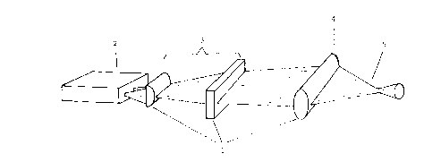
Figure 1: A diagram of a combined refractive/diffractive optical
element, calculated as an inverse marginal-value
problem.
Figure 1 shows combined refractive/diffractive optical
elements that was calculated as an inverse marginal problem. The
arrangement shown in Figure 1 consists of three mirrors 1, a
resonator 3 being formed from the two left-hand mirrors 1 in
Figure 1; this is arranged after a diode bar 2, that in this case
has a power of 50 Watts. A secondary beam shaper 4 that generates
a power density 5 of greater than 5 Megawatts per square
centimetre (35W/30~m m) is adjacent to the resonator. In this
embodiment, the single emitters are shown as diode bars 2
although they can be in the form of single diodes or a diode
matrix. The arrangement shown in Figure 1 is one example of an
arrangement; for example, the single emitters can also be
arranged between two or more mirrors 1. What is important is
that at least one of these mirrors 1 has a special, non-spherical
surface (internal corrector element). As an alternative, the
mirror 1 can be spherical although there will then be at least
one non-spherical phase plate in the path of the resonator beam
6
CA 02285134 1999-10-OS
as an internal correct element. Outside the resonator, an
additional system of matched phase plates (external generalize
lenses), transforms the emitted beam into the desired
amplitude/phase distribution.
The internal correction elements are constructed by a
global optimization method, or the internal correction elements
and the external generalized lenses are constructed together by a
global optimization method, as is described in the publication
that appeared in Science, Volume 220, for example. In this
connection, the shape of the resonator mirror 1 is optimized
until such time as it satisfies a pre-described set of
mathematically formulated requirements, in the sense of a set
criterion. The demands cited in the task can be introduced into
the set of requirements, as can additional marginal conditions
such as, for example, special properties of the mirror
manufacturing process. It is clear that, generally speaking,
not all of the criteria of the list can be satisfied. Because of
the fact that one assigns different weights to the single
criteria, different solutions can nonetheless be achieved.
Using this method, for all practical purposes, a characteristic
mode with small losses can be prepared, whereas the remainder of
the mode spectrum is burdened with many losses. This means that
single mode emission can be achieved. The mirrors 1 of the
associated resonator 3 are no longer spherical and the mode
spectrum is no longer in the class of the Hermite-Gaussian modes.
As a singular element of the characteristic value spectrum, the
7
CA 02285134 1999-10-OS
emitted mode does however display a stationary phase
distribution. As already discussed, this is a major and
important factor, for in this way a beam can be transformed into
any distribution by a generalized lens system, and in particular
into a Gaussian distribution. Thus, in summary, it can be said
that in principle, the present method or the present device is
based on the following factors:
The single emitters are set between two or more mirrors
1 as single diodes, a diode matrix, diode bars, or the like.
At least one of these mirrors 1 has a special, non-
spherical surface (internal correction element). As an
alternative, the mirrors 1 can be shaped so as to be spherical
although, in this case, at least one non-spherical phase plate
(internal correction element) will be located in the path of the
resonator beam. Outside the resonator 3, an additional system,
for example in the form of a secondary beam shaper 4 of matched
phase plates (external generalized lenses) transforms the emitted
signal into the desired amplitude/phase distribution with the
desired power density 5.
The internal correction elements are constructed by a
global optimization method, or the internal correction elements
and the external generalize lenses are constructed together by
means of a global optimization method.
The following special features are to be taken into
account when strip diodes are used:
R
CA 02285134 1999-10-OS
The strip diodes are already single mode in one spatial
direction. This means that the internal and the external
correction elements need only have a single-dimensional structure
(parallel line pattern or cylindrical surface). This makes the
lithographic method particularly attractive for manufacturing the
correction elements. The internal correction elements can thus
be applied or etched directly onto the surfaces of the diodes
(corrugated end surfaces).
In the case of vertically emitting diodes (VCSEL) the
emission becomes transversely multi-modal once the emitting
aperture exceeds a few Vim. Higher emission powers are achieved
by using VCSEL matrices. The correction elements then have a
two-dimensional structure. An alternative to this structure is
that the internal resonator correction elements is the laser
diode crystal, the surface of which is provided with a phase-
shifting relief.
9
CA 02285134 1999-10-OS
'REFERENCE NUMBERS FOR DRAWING:
1 Mirror
2 Diode bars
3 Resonator
4 Secondary beam shaper or system
Power density