Note : Les descriptions sont présentées dans la langue officielle dans laquelle elles ont été soumises.
CA 02285273 1999-09-24
WO 98/43292 1 PCT/SE98/00508
Trench Isolation
Technical Field of the Invention
The present invention relates to isolating trenches and methods of producing
such
trenches.
Description of related art
In order to isolate components in integrated circuits from each other refilled
trench
structures have been developed. There are many different ways of forming such
trenches which can be etched through a silicon layer into an underlying buried
insulating oxide layer or through a silicon substrate into an underlying
silicon layer
which has the opposite type of doping in relation to the layer which is to be
laterally
insulated. Methods of making such trenches are shown in Wolf, S., "Silicon
Processing for the VLSI Era Volume II", pages 45-56, ISBN-0-961672-4-~, 1990,
Lattice Press USA.
A problem with the use of trenches for isolating components is that the small
width
of the trenches make them vulnerable to foreign particles or defects in the
material,
both of which can short circuit the desired electrical insulation. This is
particularly
difficult to cure in the case of components having long total trench lengths.
Another
problem with trench structures is that the different thermal properties of the
materials in and surrounding the trenches can lead to mechanical stresses
occurring
in the trench material or the surrounding silicon. A further problem with
trench
structures is that steps are often formed over trenches during their
manufacture.
These steps can trap conductive material in undesirable regions during
subsequent
processing and can cause short circuits. An example of such undesirable
conductive
material is polysilicon strings which remain in the trench edges and can go
all the
way around a component. These strings can then cause short circuits between
two
conductors which cross the trench and are in contact ~.vith the strings.
CA 02285273 1999-09-24
WO 98/43292 ~ PCT/SE98/00508
S ummery
An object of the invention is to produce trench structures with a reduced risk
for
short-circuiting crossing conductors and a greater tolerance of foreign
particles and
defects in the material.
In accordance with the invention, this is achieved by means of a trench
structure
having a segmented structure.
A trench formation formed in accordance with the invention has a number of
advantages. One advantage is that a short circuit can only occur if two
defects or
foreign panicles occur close to each other. This risk is considerably lower
than the
risk that two defects or foreign particles occur on a simple trench which
completely
surrounds a component.
Another advantage is that the reduced length of the islands of silicon
surrounded by
the trenches helps relieve the mechanical stresses which are generated during
subsequent processing and use.
A further advantage is that there is a reduced risk that conducting residues.
for
example strings of polysilicon, remaining from later process steps surround
the
insulated device and short circuit conductors which cross the trench.
Yet another advantage is that the thermal insulation of the trench formation
according to the invention is greater than that of a single trench and thus
the
conduction of heat to components surrounded by a trench formation according to
the
present invention is reduced.
CA 02285273 1999-09-24
WO 9S/43292 3 PCT1SE98/00508
Brief Description of the drawings
The invention is described below by means of examples of embodiments which are
illustrated in the following figures in which:
figure 1 a) shows a plan view of a prior art trench structure,
figure lb) shows an enlarged view of a cross-section along line I-I in figure
la,
figure 2a) shows a plan view of one embodiment of a trench structure according
to
the invention,
figure 2b) shows an enlarged view of a cross-section along line II-II of the
trench
structure show in figure 2a,
figure 3a) shows a plan view of a second embodiment of a trench structure
according to the invention,
figure 3b) shows an enlarged view of a part of the trench structure of figure
3a}.
figure 4 shows a third embodiment of a trench structure according to the
invention.
1J
Detailed description of the Embodiments
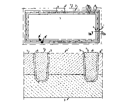
In the prior art trench structure shown in figure 1 a wafer 1 for producing
semiconductor devices has a layer 2 of, for example, doped silicon, for
example, n-
?0 type doped silicon over a layer 3 of oppositely doped, in this case p-type,
silicon.
The wafer has a continuous or closed-loop trench 4. This trench 4 has a U-
shaped
cross-section which extends from the upper surface of wafer 1 through layer 2
into
layer 3. Trench 4 has insulating walls ~ made of, for example, oxidised
silicon and a
filling of polysilicon 6 between the trench walls 5. Trench 4 extends along
the
boundary between an island 7 of n-type doped silicon and the rest of the n-
type
doped silicon 2 and insulates it from the rest of the n-type doped silicon 2.
This
island 7 can be used as the foundation for one or more components (not shown)
such as resistors, capacitors, diodes, transistors and other bipolar
components. In the
event of a conducting foreign particle or defect in the material (which for
the sake of
30 brevity will be called foreign particle from now on} 8 bridging the trench
4 then
CA 02285273 1999-09-24
WO 98143292 ~ PCT/SE98100508
island 7 will be in undesired electrical contact with layer 2 and the function
of any
components) formed on or by island 7 will be adversely affected.
Figures 2a) and 2b) show an embodiment of a trench structure according to the
present invention. In this embodiment f rst closed Ioop trench 4 is surrounded
by a
second closed loop trench 4' and separated from it by an island or slice of,
for
example, n-type doped silicon 2'. The invention is not limited to silicon
based
components but can be adapted as required for use with any material. It is
also
possible to adapt it for use with other manufacturing processes such as
silicon on
insulator (SOI) technology in which a layer of silicon is provided on a
insulating
substrate made of, for example, silicon oxide. Trenches 4, 4' have insulating
walls ~
made of, for example, oxidised silicon and a filling of polysilicon 6 between
the
trench walls 5. The material of the insulating walls ~ can be any suitable
material
such as silicon nitrides. silicon oxides, porous silicon, sapphire, aluminium
oxide,
1 ~ aluminium nitride, diamond, quartz, other dielectric materials and
combinations of
the same and it is conceivable that a material other than polysilicon or no
material is
present between the insulating walls ~. Second trench 4' is constructed in the
same
way as trench 4 and is appropriately formed simultaneously with trench 4. It
is
joined to first trench 4 by intermediate transverse trenches 9 formed in the
slice of
?0 n-type doped silicon 2' and spaced, in this example, at predetermined
regular
intervals around the circumference of trench 4. It is naturally also possible
to have
irregularly spaced transverse trenches 9. With such an arrangement of trvo
trenches
4, 4' linked by transverse trenches 9 in a chain-like structure not only does
it need
one or more foreign particles 8' to bridge the trench 4 between island 7 and
the slice
25 of n-type silicon 2' as well as one or more foreign particles 8" to bridge
the trench
4' between slice 2' and layer 2 but also these foreign particles 8', 8" must
be
present between two adjacent transverse trenches 9 before island 7 is brought
into
electrical contact with layer 2. The risk of this occurring is substantially
less than the
risk that a single particle will bridge a single trench.
CA 02285273 1999-09-24
WO 98/43292 5 PCT/SE98/00508
The optimum number of transverse trenches 9 depends on the expected sizes of
foreign particles and how often they occur. With very rare foreign particles
then it
may be sufficient to have only two transverse trenches. As the risk of
contamination
in the form of foreign particles increases then it may become advisable to
increase
the number of transverse trenches 9.
Furthermore the Links forming the chain-like structure do not have to be
elongated
links but could be any appropriate shape such as round. oval, square.
trapezoidal etc.
Typical lengths for the trenches 4, 4' forming the sides of links could be 15-
50
micro-meters with a width of 1-3 micro-meters. The distance between t<vo
trenches
could typically be from 3- 50 micro-meters.
While the invention has been illustrated by examples in ~.vhich the trench
structure is
formed of continuous trenches it is of course conceivable that components
mounted
near the edge of a substrate would be protected by trench structures which did
not
extend along the edge of the substrate.
Figures 3a) shows an embodiment of the invention in which the problem that
residual conductive material, such as polysilicon 13, remaining along the
trench
edges can cause short-circuiting between conductors crossing the trenches can
be
avoided. Figure 3b) is an enlargement of part of figure 3a). Polysilicon 13 is
represented in figures 3a) and 3b) by solid lines on the circumference of the
shaded
trenches. Conductors 1 l, 11' at different potentials both cross trench
structures 4,
4'. If there is any un-oxidised poiysilicon remaining along the edges of the
trenches
then this will act as a conductor between conductors 11,11' and the island 7
will be
short-circuited. In order to prevent this a break 12 is formed in trench 4 in
each
portion of trench 4 which joins the conductors 1 l, 1 i'. Each break 12
extends into
one of the islands 18' formed between trenches 4, 4'. Similarly a break 12' is
formed in trench 4' in each portion of trench 4' which joins the conductors
11, 11'.
Each break 12' extends into one of the islands 18" formed between trenches 4,
4'.
These breaks 12, 12' are made by leaving a gap in the masks used to produce
the
CA 02285273 1999-09-24
WO 98/43292 ( PCTISE98100508
trenches so that the original n-type doped silicon which is oxidised. coated
with a
deposit of polysilicon and subsequently etched back during the formation of
the
trenches ~. 4' is left with an insulating layer of oxide. Normally polystrings
(that is,
continuous lengths of polysilicon) are formed at the edges of the trenches
where
there is a step in the planar surface. It has however been found that corners,
particularly convey corners lb'. which occur where the breaks meet the
trenches
cause an accelerated etching of polysilicon. This means that during the usual
process
of etching back unwanted .polysiiicon any polystrings which are present at or
near to
the comers are automatically broken by being etched away. This prevents
polystrin~s on the outside perimeter of the trenches from being in electrical
contact
with polvstrings on the inside perimeter of the trenches. Breaks 12, 12' thus
form
insulating breaks in any strings of conducting material and thereby ensure
that
conductors 11, I l' are isolated from each other. In order to ensure that the
conductors 11, 11' are isolated each trench 4 must have at least two breaks 12
in it
1 ~ and each trench 4' must have at least two breaks I2 in it. Each pair of
breaks 12,12'
must be positioned on opposite sides of a conductor 11, or 11' such that there
is no
continuous conducting path between the conductors 11, 11'. In other words. one
break must be in the long path between the conductors 11,11' which path goes
around almost all of the perimeter of island 7 and the other break must be in
the
~0 shortest path between the conductors 1 l, I I'.
In another embodiment of the invention, not shown, instead of having four
staggered breaks 12, I2' as shown in figures 3a) and 3b) it is conceivable
that the
four breaks are aligned such that appear to be form two lengthened breaks
which
2~ both extend simultaneously across both trenches 4, 4'.
As shown in figure 4, the invention could also be realised with 3 trench
structures
4, 4' ,4" of increasing size arranged around a component to be protected.
30 The invention is not limited to the embodiments described above but could
include
more than 3 trench structures. These trench structures could be all
interconnected by
_~.._ ~ r ,
CA 02285273 1999-09-24
WO 98/43292 '7 PCT/SE98/00508
transverse trenches or alternatively could be interconnected into groups
wherein
each group is not interconnected to the other group or groups.
In order to realise the full electrical isolating benefits of a trench
structure according
to the invention. it is preferable that the islands 2' formed between the
trenches 4,
4',9 should be designed to not be in electrical contact with any active
conductors 11.
11' although it may be necessary to provide them with a connection to earth.
Thus
the masks used during processing of the wafer 1 should not have any contact
holes
between the islands 2' and any active conductors 11, I 1'.
As well as providing improved electrical insulation a trench structure
according to
the invention provides increase thermal insulation between the components on
either
side of it.
1 ~ Furthermore the provision of transverse trenches provides multiple paths
for the
relief of stresses. The reduces the risk of stress damage occurring as the
stress
travels a shorter path before being relieved.
The insulating material can be any suitable material such as silicon nitrides,
silicon
oxides, porous silicon, sapphire, aluminium oxide, aluminium nitride, diamond,
quartz. other dielectric materials and combinations of the same.
According to a further embodiment of the invention the trench structures
surround a
silicon-based or other semiconductor-based substrate and extend down to a
buried
2~ isolating layer to form a complete galvanic isolation around the substrate.
The
buried isolating layer can natural be formed of any suitable insulating
material.
including that used for the trench structures.