Note : Les descriptions sont présentées dans la langue officielle dans laquelle elles ont été soumises.
CA 02285355 1999-09-28
WO 98144626 PCT/DK98I00133
Pulse referenced control method far enhanced
power amplification of a pulse modulated signal
Technical field
This invention relates to power amplification of pulse modu-
lated signals by a switching power stage. The invention may
advantageously be used for improved conversion of a digital
signal directly to analog power. Applications are direct
digital audio power conversion and general DC-DC or DC-AC
power conversion systems controlled from the digital domain.
Background
The advantages of power amplification based on a switching
power stage are well known. The high efficiency provides sev-
eral advantages, in terms of minimal weight and volume,
higher power handling capability and improved reliability.
The fundamental elements in switching power amplification are
the modulator, the switching power stage and the demodulation
filter to reconstitute the modulated signal. The non-
linearity of the switching power stage presents a significant
impediment to maintain the modulator performance throughout
the subsequent power conversion by a switching power stage.
This problem is fundamental and independent on the use of
analog modulation as analog PWM, or digital modulation as di
rect digital PCM-PWM conversion.
In prior art, compensation for the non-ideal behavior has
generally been attempted with various feedback control meth-
ods. US Patent no. US4724396 and US Patent no. US5521549 dis-
closes examples of this method with audio power amplification
as specific application. However, linear feedback control
methods require an analog low frequency reference. It is de-
sirable with a more direct digital source to power conversion
' to simplify the power conversion in that no separate D/A con
verter is needed. Furthermore, analog modulation circuitry
and carrier generators will not be required. International
patent application no. W092/11699 and international patent
application no. W097/37433 discloses improved methods for
SUBSTITUTE SHEET (RULE 26)
.
CA 02285355 2003-09-09
2
digital PCM-PWM conversion for digital to power
amplification. In practice, these systems are hardly easy
to implement, since compensation for the fundamental error
s sources within the switching power conversion are not
provided. The application of digital feedback control
referenced to the digital source is complicated in that an
analog-digital converter is needed in the feedback path.
This renders normal feedback control impractical.
to
The published international patent application EP758164
discloses a feedback method local to the switching power
stage, in which the power stage output is feedback and
summed with a pulse width modulated input. The resulting
15 signal is used to drive the switching power stage. The
compensation effect however will be limited and it is
difficult to control the improvements towards all error
sources.
2o In conclusion, no invention in prior art exist for general
power amplification of a pulse-modulated signal, that
incorporates simple and effective means to eliminate any
source of non-linearity and noise in the switching power
amplification stage.
Accordingly, an objective of the present invention is to
enable improved power amplification of a pulse modulated
signal, where all error sources related to the power stage
and demodulation filter are eliminated, such that the
modulator performance can be maintained throughout the
subsequent elements all the way to the output. Another
objective of the invention is to provide a practical
digital PCM-power conversion system, that is insensitive to
CA 02285355 2003-09-09
3
power stage non-linearity, perturbation on the power supply
and any other non-ideal elements.
SUMMARY OF THT IN'VTNTION
The objectives of the invention are achieved by the
introduction of a correction unit in-between the pulse
modulator and the switching power amplification stage. The
l0 correction unit provides compensation by means of pulse re-
timing on the pulse edges, said re-timing controlled to
have a "predistorting" effect, such that the resulting
switching power stage output is free from distortion, noise
or any other undesired contribution.
One preferred embodiment of the invention is particular in
that pulse re-retiming in the correction unit is a linear
function of an error signal input. This is advantageous in
that the resulting control system is linear, whereby system
2o design and optimization is simplified and the performance
improvement controllable.
It is expedient that the pulse reference control system
comprises the following fundamental elements:
An input terminal taking a pulse modulated signal.
A Correction Unit with means to correct the delays of the
individual pulse edges, controlled by a control input.
A state feedback with compensation.
A reference-shaping block to modify the pulsed reference
3o input for optimal error estimation.
A difference block to generate an error signal and a
compensator to shape this error. The invention includes
CA 02285355 2003-09-09
3a
various embodiments regarding actual realization of the
control function within the correction unit.
The invention includes various advantageous embodiments
concerning improved digital-analog power conversion
suitable for audio power amplification. The reference
input can be modulated by pulse width modulation. The
state feedback can be the local switching power output
voltage vP and the reference shaping block can be unity.
to Alternatively, the state feedback can be the local
switching power output, the feedback compensation can be a
first order filter, and the reference shaping block equally
can realize a first order system. Alternatively, the state
feedback can be the global amplifier output, the reference
shaping block can be a second order filter and the feedback
path compensation can be a constant attenuation.
The switching power stage output can directly drive a
loudspeaker or other load with pulses directly from the
2o switching power stage.
The invention is a fundamentally new control method for
improved amplification of a pulse modulated input
signal. The application range is extremely broad in
that the invention can be used with any pulse-modulated
input, modulated in the analog or digital domain, and
feed any load where a pulsed power signal of
controllable quality is needed. Ultimately,
CA 02285355 1999-09-28
WO 98/44626 4 PCT/DK98/00133
the principle of the invention may realize perfect reproduc-
tion of the pulsed reference such that the output is a con-
stant times the input, independent on any disturbances that
is introduced during power conversion.
BRIEF DESCRIPTION OF THE DRAWINGS
The invention will be further described with reference to the
drawings in which:
Fig. 1 shows a principle of power amplification based on ei-
ther analog or digital input that is well known to the art.
Fig. 2 shows a method of power conversion based on digital
pulse modulation. This approach is well known to the art.
Fig. 3 shows a general model of the invention.
Fig. 4 shows a preferred embodiment of the invention, in
terms of a dual input pulse referenced control method based
on state feedback from the power stage.
Fig. 5 shows various embodiments of the invention regarding
pulse edge delay error correction methods.
Fig. 6 shows the principle for one preferred embodiment of
the invention regarding edge delay correction unit implemen-
tation that implements the expedient linear control function,
by operating on both edges of the pulse.
Fig. 7 shows a system block diagram for one preferred imple
mentation for a double-sided edge delay correction unit.
Fig. 8 shows an advantageous application of the invention, in
terms of a digital - power conversion system for audio pur-
poses, where the reference shaping block R is unity and the
feedback block A has a constant attenuation characteristic.
Fig. 9 shows a linear model for the advantageous application
SUBSTITUTE SHEET (RULE 26)
r ,.
CA 02285355 1999-09-28
WO 98/44626 PCT/DK98/00133
of the invention in Fig. e. The model defines an appropriate
compensator for the application.
Fig. 10 shows yet another advantageous embodiment of the in-
5 vention, in terms of a digital - power conversion system for
audio purposes, where the reference shaping block and feed-
back block have first order characteristics to improved error
estimation.
Fig. I1 shows yet another advantageous embodiment of the in-
vention, in terms of a digital - power conversion system for
audio purposes, where a global feedback source is used for
error correction.
Fig . 12 shows the control loop characteristics for one pre-
ferred design approach for the preferred embodiment of Fig.
8.
Fig. 13 shows the closed loop system characteristics for one
preferred design approach for the preferred embodiment of
Fig. 8.
Fig. 14 shows the results of a simulation of error correction
towards a deterministic pulse timing error source in the
switching power stage. The example embodiment of the inven-
tion reduces the distortion considerably.
Fig. 15 shows a simulation of the effects of power supply
perturbations. The example embodiment of the invention elimi
notes the intermodulation caused by this error source.
DETAILED DESCRIPTION
To fully understand the invention it is helpful to discuss
the fundamental physical limitations that lies within ampli
fication of a pulse modulated signal to power levels. Most
problems relate to the switching power stage that serves to
amplify the pulses coming from the modulator. It is expedient
to divide the error sources in to pulse timing errors (PTE)
SUBSTITUTE SHEET (RULE 26)
CA 02285355 1999-09-28
WO 98/44626 PCT/DK98/00133
s
and pulse amplitude errors (PAE). Pulse Timing Errors arise
f rom
~ Delays from turn-on or turn-off to the actual transition at
the output of the switching power stage are different in
the turn-on and turn-off case. The delays depend on various
parameters in the power switch physics and in the hardware,
that drives the switches.
~ The delay between a turn-off and the following turn-on in a
switching leg.
Z0 ~ The finite rise- and fall-times as opposed to the infi-
nitely fast switching required by theory.
Pulse Amplitude Errors (PAE) mainly arise from:
~ Noise from the power supply that feeds the switching power
15 stage. Any power supply ripple or noise will intermodulate
with the modulated audio signal, and the switching power
stage has a Power Supply Rejection Ratio (PSRR) of OdB.
~ Finite impedance for the power switches.
~ High frequency resonant transients on the resulting pulse
20 power signals.
There are additional error sources relating to the non-ideal
modulation and non-ideal demodulation. The demodulation fil-
ter errors may introduce further distortion, since magnetic
25 core materials are not ideal. In addition, the filter in-
creases the total output impedance. Accordingly, changes in
load impedance will distort the frequency response.
Fig. 1 shows a method, well known in the art, to realize
30 power amplification based on analog pulse modulation tech-
niques. The modulator output feeds a switching power stage,
the output of which is demodulated and feed to the load. A
linear control system referenced to the analog input se nres
to minimize the errors within the power conversion, such that
35 the effects of the above mentioned errors can be minimized. A
digital input requires a separate D/A converter to generate
the analog input that serves as input to the control system.
Fig. 2 illustrates the simplified and desirable system for
SUBSTITUTE SHEET (RULE 26)
fi ,.
CA 02285355 1999-09-28
WO 98/44626 PCT1DK98100133
7
direct digital to analog power conversion using digital pulse
modulation techniques, also well known in prior art. The ap-
plication of error feedback control is complicated in that an
analog/digital converter would be needed to enable comparison
with the digital reference source. This compromises both per-
formance and complexity and renders the method impractical.
The new principle of the invention is shown by the general
block diagram in Fig. 3. The modulator is feed to a correc-
to Lion unit that serves to correct or "predistort" the pulse
modulated signal v, to generate the compensated pulse signal
v~, such that the said non-ideal behavior within the subse-
quent power conversion and demodulation are eliminated. This
is carried out by means of intelligent pulse edge delays on
each of the pulse edges, controlled by an input control sig-
nal ve to the correction unit . The method will henceforth be
referenced to as Pulse Edge Delay Error Correction (PEDEC).
The invention is a fundamentally new control method for im-
proved amplification of a pulse modulated input signal. The
application range is broad in that the invention can be used
with any pulse-modulated input, modulated in the analog or
digital domain, and feed any load where a pulsed power signal
of controllable quality is needed.
The invention relies on two fundamental facts:
~ The pulse modulator can generate a very high quality
pulsed waveform, that may be used 'as reference for the
control system.
~ All error sources (PAE or PTE) within the switching power
conversion can be corrected by intelligent pulse re-timing
and all error sources only need minor pulse edge re-timing
for perfect elimination.
The edge correction may be implemented using single-sided or
double-sided edge delay correction, as shown conceptually in
Fig. 5. The choice of single or double edge correction is in-
dependent of the type of modulation method. The control of
SUBSTITUTE SHEET (RULE 26)
CA 02285355 1999-09-28
WO 98/44626 PCT/DK98/00133
8
both edges leads to efficient correction and furthermore has
simple implementation strategies. Subsequently, the following
description of this aspect of the invention will focus on
double edge correction.
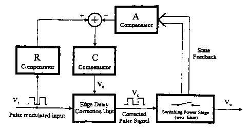
One preferred embodiment of the invention is shown Fig. 6.
The dual input pulse referenced feedback control system com-
prises:
- An input terminal that is feed by a pulse modulated refer-
ence signal yr .
- A Correction Unit (PEDEC unit) with means to control the
delays of the individual pulse edges and generate the cor-
rected output pulse signal v~.
- A state feedback block A including compensation from the
power stage block.
- An optional reference shaping block R.
- A subtraction unit to derive error information.
- A compensator C to shape said error and feed the Correc-
tion Unit with said shaped error ve.
The correction unit may be realized by various linear and
also non-linear methods. A particularly advantageous embodi-
ment of the invention regarding PEDEC unit realization is de-
scribed hereinafter. It proves advantageous to let the con-
trol error signal ve to the PEDEC unit realizes an effective
change in pulse width orw at the end of each switching cycle
that is proportiona2 to the control signal input ve:
dtW _ k
dye w
(1)
By averaging within a single switching cycle, the relation
ship between an increment in pulse width arW and the corre
sponding change in the average of the PEDEC unit output e~~
can be established. Assume for simplicity in the following
that the PEDEC unit output pulse amplitude is unity. o~~ is
3 5 related to OtW as
SUBSTITUTE SHEET (RULE 26)
CA 02285355 1999-09-28
WO 98144626 PCT/DK98/00133
9
d~r,+~rw t,
DVe=t~ jl'dl+ J(-1)'dI = 2Lll", (2)
0 d~t,+tuW
Where d is the duty-cycle within the present switching cycle
and is is the switching period. Hence:
_~~ _ _2
dt", is (3)
S
Combining and (1) and (3), the linear control function ar-
rives:
_ _dv~ _ 2kw
kPEDEC dye IS ( 4 )
This preferred linear control function is advantageous in
that it simplifies controller design and provides controlla-
ble performance improvements compared to e.g. the implementa-
tion of a non-linear control function.
A preferred embodiment of the invention is particular in that
the implementation of a double-sided correction unit that im-
plements (4) is simple. The method is shown in Fig. 6. The
linear control function is realized by a limited integration
of the reference v" thus generating the signal v;. A com-
parison between the modified reference with the control sig-
nal ,~e caused the pulse edges to be re-timed. From Fig. 6 in
follows that:
tw-tw-tOVe ~
r t0 we~~~ (5)
~l", = ft - ft = ldVe ( I S Ve S 1)
-t0 we~j~
SUBSTITUTE SHEET (RULE 26)
- CA 02285355 1999-09-28
WO 98/44626 PCT/DK98/00133
Where (~) indicates the corrected variable after passing the
PEDEC unit. It is assumed that all pulse amplitudes are nor-
malized to unity. In this preferred implementation, kW as de-
fined in (1) is:
5
dtw
kw ._ dv _- to
a (6)
The following equivalent control gain emerge for the proposed
implementation of double sided edge correction:
~o
kPEDEC- t
s (~>
to
Fig. 7 shows a preferred implementation of the double-sided
edge correction method. The method is very simple and
straightforward.
For optimal control in this preferred solution, the pulses
should have a certain minimal width. The minimum pulse width
for optimal performance is related to the modulation index M
and switching period is as:
21
0
tw,min ~ tp ~ M~ = 1 - t
s
This constraint on pulse width and maximal modulation index
Mr"aX does not present a fundamental limitation, since the
correction still will work partially beyond this limit. Since
only a limited correction range is generally needed, ro is
preferably on order of magnitude or more lower that r,.
The invention includes several embodiments regarding the ap-
plication of the invention specifically in digital to analog
power conversion. One preferred embodiment is the system
shown in Fig. 8. Using PEDEC in combination with one of the
high performance digital pulse width modulation methods (PCM-
SUBSTITUTE SHEET (RULE 26)
CA 02285355 1999-09-28
WO 98/44626 PCT/DK98/00133
11
PWM methods) that are known to the art, the signal will re-
main digital or pulsed throughout the main audio chain. No
analog modulator or carrier generator is needed as with ana-
log pulse modulation, since the system is controlled exclu-
sively by the digital modulator. In this particular embodi-
A
ment of the invention, the state feedback is a voltage feed-
back from the switching power stage output vp. The feedback
path compensator is a simple attenuation, and the compensator
block C(s) is a linear filter. Despite the simple controller
structure of this particular embodiment, the system intro-
duces a very powerful and flexible control of system perform-
ance.
The preferred linear control function provides great flexi-
bility in performance optimization. An example of PEDEC con-
trol system design is specified in the following. The compen-
sator is defined in the linear model of the system as shown
in Fig. 9. The PEDEC unit has been replaced by its equivalent
linear gain and the resulting system has been redrawn to em-
phasize the dual input character of the PEDEC based digital
to power conversion system. The specified compensator pro-
vides sufficient flexibility to optimize the performance to
various characteristics. The resulting loop transfer function
is derived directly from the system model:
L(s) = Kpk~DEC C(S)
KCKpkpgDEC T.~S+I (9)
K (t p~S t 1)(T pzS + I)(T ~~S t I)
All non-ideal effect as noise, distortion or power supply
perturbations that influence the power stage gain Kp are re-
duced by the sensitivity function S(s)=(1+L(s))-~ . The actual
loop shaping is a compromise between loop bandwidth and the
desired sensitivity function. Further considerations are sta-
bility and robustness to uncertainty in system parameters.
Table 1 gives as eet of normalized system parameter values
that will lead an appealing compromise between these aspects.
SUBSTITUTE SHEET (RULE 26)
CA 02285355 1999-09-28
WO 98/44626 PCT/DK98100133
12
The compensator DC gain K~ is optimized to yield the desired
loop bandwidth. A bandwidth of 6-8 times target bandwidth is
a good compromise between efficiency and error correction ca
pability. Fig. 12 shows Bode plots for each component and the
resulting loop transfer function.
Parameter Value Coa~ent
kPEDEC 0 2 Equivalent PEDEC unit gain.
K 10 System gain = 20dB
KP 10 Equivalent power stage gain = 20dB
I" 6 Bandwidth
--L j Loop parameter
fV~ 2aipi
20
j Loop parameter
P 2m P
20
2j~ Loop parameter
P~ 27CS
P
S
j Loop parameter
In = a
tat =, 2
ff 2 Filter natural frequency
Qf I Filter Q (Bessel characteristic)
1 ~,xample or rrequency normalized parameters
The gain of the system is controlled by the A-block, and with
the given example embodiment, the PEDEC control system will
force the system gain to be constant within the target band-
width. This stabilizes both system gain and the frequency re-
sponse. According to the linear model for this example em-
bodiment of the invention in Fig. 9, the resulting system re-
sponse is constituted of two contributions, since the refer-
ence has two inputs in the loop. The system transfer function
is:
SUBSTITUTE SHEET (RULE 26~
r i
CA 02285355 1999-09-28
WO 98/4A626 fCTIDK98100133
13
H(s) = C(s)xPkPEDEC + Kp
1 + L(s) 1 + L{s) ( 10 )
X,,
K p ~C ( s )k pEDEC '~ I
I + L(s)
In the 'special (but not unusual) case where x=Kp the system
transfer function is constant:
H(s) = xLC(S)lCpEDEC +' i~ = K ( I1 )
1 + C(S)h pgDEC
In the general case:
cr<r~) (la)
hp (I » I~)
Fig. 13 shows the resulting Bode plots for the closed system,
consisting of two contributions forming the loop response and
a total system response with the demodulation filter. The
constant gain characteristic of the loop caused by K=xP. The
demodulation filter exclusively determines the response of
the system.
The parameters of the example embodiment above are only il-
lustrative and various other system characteristics can be
devised by other loop transfer function gain / bandwidth com-
promises etc.
Other advantageous embodiments, also suitable for high qual-
ity digital to power conversion are shown Fig. 10 and Fig.
11. These alternative embodiments are characterized by using
different compensator and reference shaping blocks. The em-
bodiment in Fig. 10 is preferably based on a first order
characteristic in both the reference shaping block R(s) and
the feedback compensator A(s). The advantages in the demodu-
lation of both reference and feedback signal are minimized
noise within the control system and furthermore lower band-
SUBSTITUTE SHEET (RULE 26)
CA 02285355 1999-09-28
WO 98/44626 PCT/DK98/00133
24
width requirements for the feedback compensator. The embodi
ment in Fig. 11 is based on a global feedback source such
that demodulation filter errors are included within the loop
and also corrected for. This requires a second order refer
s ence shaper for optimal error estimation.
The correction effects towards pulse timing errors (PTE) is
shown in Fig. 14, where THI? for the open loop system and
three PEDEC controller configurations have been investigated
at the worst case signal frequency. Clearly, the controller
considerably reduces the effects of this particular error
source. Furthermore, adjusting the compensator gain K~ can
control the improvements. In this particular situation the
distortion is reduced 20dB - 30dB. Fig. 15 shows an investi-
gation of PAE with a severe power supply perturbation of 10
Vpp. Top figure visualizes the clear intermodulation between
power supply and signal. Bottom figure shows how the PEDEC
controller eliminates this effect such that the intermodula-
tion is no more visible in the time domain. The intermodula-
tion distortion is reduced more than 40dB compared to the
open loop case, as predicted by the sensitivity function in
theory.
Although the invention is described hereinbefore with respect
to illustrative embodiments thereof, it will be appreciated
that the foregoing and various other changes, omissions and
additions may be made without departing from the spirit and
scope of this invention.
SUBSTITUTE SHEET (RULE 26)
~ r ,.