Note : Les descriptions sont présentées dans la langue officielle dans laquelle elles ont été soumises.
CA 02288605 1999-11-08
COMPLIANT LEADS FOR AREA ARRAY
SURFACE MOUNTED COMPONENTS
FIELD OF THE INVENTION
The present invention generally relates to interconnection elements for
interconnecting
integrated circuit packages to printed circuit boards in surface mounted area
array assemblies,
using flat connection elements of particular configurations and arrangements.
BACKGROUND OF THE INVENTION
In the field of integrated circuit packages, area array integrated circuit
packages are becoming
more and more frequently used. Area array packages include ball grid arrays
and column grid
arrays. The main advantage of the area array products is the large number of
I/O contacts which
are provided as the complete bottom surface of the module or package is used,
in comparison
with the peripheral lead products, which make use of only contact locations
adjacent to the
periphery of the package. These products are attached to printed circuit
boards using established
surface mount techniques. Area array packages include packages with either
fully or partly
populated bottom surfaces.
In preparation for surface mounting on a printed circuit board for example,
solder balls or solder
columns are permanently attached to the IC package, which in turn are
permanently attached to
the printed circuit board pads by soldering. The assembled structure includes
interconnect
elements, for example solder balls, with two solder joints, one to a contact
on the package
surface, one to a contact on the printed circuit board surface.
One major restriction of the area array interconnection technology is the
reliability of the solder
joints. An assembled product is subjected to thermal variations with
significant stresses resulting
in the solder joints because of the difference in thermal expansion between
the printed circuit
board and the IC package. This results from the differences in the coefficient
of thermal
CA9-1999-0032 1
CA 02288605 1999-11-08
expansion of the elements involved. Different factors, including operating
temperature of the
assembled product, compliance of the interconnection elements, number of
thermal cycles, size
of the package, package material, have an impact on the amount of resulting
stress on the solder
joints. Improvements in reliability are needed for the more extreme conditions
and critical
factors.
One method to reduce stress in the solder joints is to increase the compliance
of the
interconnection element. For example, instead of using a solder ball, a well-
known solution is to
use a solder column interconnecting element. Assembled solder ball connections
provide short
cylindrical interconnections, compared to solder columns which provide much
longer cylindrical
connections, typically in the order of three times longer. Longer cylindrical
connections are
more compliant, so lower stress is transmitted to the solder joint.
' There are important drawbacks with the use of solder column
interconnections. With longer
connection elements, the resulting product is more susceptible to damage
resulting from
handling. Longer elements result in an increase of the self inductance of the
connections, which
is detrimental to the electrical performance of the IC package. It would be
preferable to use a
connection element that is more compliant than solder ball but with a length
equivalent to a
solder ball.
Flat leads can be more compliant than cylindrical connections such as balls or
columns. In the
past, flat leads have been used extensively as interconnection elements in
peripherally connected
products such as quad flat packs. U.S. patent 5,647,124 which issued July 15,
1997 to Chan et al
entitled "Method of Attachment of a Semiconductor Slotted Lead to a
Substrate"; U.S. patent
4,647,126 which issued March 3, 1987 to Sobota entitled "Compliant Lead Clip";
and U.S.
patent 5,317,479 which issued May 31, 1994 to Pai et al, entitled "Plated
Compliant Lead",
provide examples of the use of flat leads in peripheral connection packages.
For today's high
density IC packages, peripheral connection packages are not practical because
they do not offer a
CA9-1999-0032 2
CA 02288605 1999-11-08
sufficient number of I/O connections, because of the inherent configuration
where only the
outside peripheral area of the packages is used to connect to the printed
circuit card.
In the patent literature, there have been some descriptions of the possible
use of flat leads in area
array packages. US patent 4,751,199 which issued June 14, 1999 to Phy,
entitled "Process of
Forming a Compliant Lead Frame for Array-Type Semiconductor Packages" teaches
the use of
flat leads on an area array IC package. A drawback with this disclosed
approach is that all leads
are aligned in the same direction. In actual conditions stresses result in
directions extending
radially outward from the center of the module. Disposition of the leads on
the package must be
optimized in order to get low stress on the joints and appropriate reliability
with a flat lead
arrangement on an area array package. These are some of the shortcomings of
this reference
subsequently addressed by the subject invention.
U.S. patent 5,420,461 which issued May 30, 1995 to Mallik et Al., entitled
"Integrated Circuit
Having a Two-Dimensional Lead Grid Array" shows a configuration very similar
to what is
disclosed in Phy, and suffers from the same drawbacks. The leads are all
aligned in the same
orientation, which has been found to be not optimal.
Also of interest are the teachings of US patent 5,490,040 which issued
February 6, 1996 to
Gaudenzi et al and entitled "Surface Mount Chip Package Having an Array of
Solder Ball
Contacts Arranged in a Circle and Conductive Pin Contacts Arranged Outside the
Circular
Array". The point of neutral stress of an array is discussed and the
recognition that the degree of
stress in the leads and contacts in a circuit package radiate from this
neutral point. Thus it is
proposed in this reference that ball contacts should only be used up to a
certain radial distance
from the neutral point, and further out, pin connections should be used in
order so that the effects
of stress can be minimized.
CA9-1999-0032 3
CA 02288605 1999-11-08
SUMMARY OF THE INVENTION
It is one object of the present invention to provide an area-array integrated
circuit package with
increased reliability in the interconnections in the presence of thermal
stress.
It is a further object of this invention to provide a new, practical and more
reliable compliant
interconnection element for interconnecting electronic circuit components.
It is another object of this invention to provide flat, compliant, connecting
elements, or leads,
which are oriented in an IC package such that each flat lead faces the neutral
point of the
package. The flat connection elements are aligned in the orientation of
optimal compliance and
flexibility, thereby offering compliance to thermal variation that is superior
to that of commonly
used solder balls or columns.
It is another object of the present invention to provide interconnections from
one planar substrate
to another, where the substrates may be printed circuit boards, ceramic cards,
or other substrates
common in the field.
According to one aspect of the invention there is provided an integrated
circuit package having
an array of contacts on a surface of the package and said array of contacts
has a neutral point. A
plurality of compliant leads is provided such that each lead is connected to
one of said contacts
on the surface of the package. Each lead extends outwardly from a respective
contact on said
surface and has a generally rectangular cross-section shape such that each
lead has a width
dimension and a thickness dimension wherein the width dimension is greater
than the thickness
dimension. At least some of the leads are arranged and oriented around the
neutral point of said
array such that the width dimension of said at least some of the leads face
the neutral point.
According to another aspect of the invention, there is provided an electronic
circuit assembly
comprising a first planar component having an array of contacts on one surface
such that said
CA9-1999-0032 4
CA 02288605 1999-11-08
array of contacts has a neutral point and a second planar component having
array of contacts on
one surface thereof such that said array of contacts on the surface of the
second planar
component correspond to the contacts in said array of contacts on the surface
of the first planar
component. A plurality of compliant leads is provided such that each contact
on the surface of
the first planar component is interconnected by a compliant lead to a
corresponding contact on
the surface of the second planar component. Each compliant lead has a
generally rectangular
cross-section shape such that each lead has a width dimension and a thickness
dimension such
that the width dimension is greater than the thickness dimension. At least
some of the compliant
leads are arranged and oriented between the contact on the surfaces of the
first and second planar
components around the neutral point such that the width dimension if said at
least some of said
compliant leads face said neutral point.
Further details and advantages of the invention will be apparent from the
following description
of the preferred embodiments of the invention, illustrated in the accompanying
drawings.
CA9-1999-0032 5
CA 02288605 1999-11-08
BRIEF DESCRIPTION OF THE DRAWINGS
Figure 1 is a side cross-sectional view of a prior art IC package assembled on
a printed circuit
card.
Figure 2 is a top schematic view of an IC package assembled on a printed
circuit card, showing
the direction and relative importance of stresses resulting from thermal
deformation as known in
the prior art.
Figure 3 is an isometric view showing a prior art cylindrical connection
element.
Figure 4 is an isometric view showing a flat connection element which is a
feature of the present
invention.
Figure 5 is a top view of an IC package according to a preferred embodiment of
the invention.
Figure 6 is a side cross-sectional view of an IC package assembled on. a
printed circuit card,
according to a preferred embodiment of the invention.
Figure 7 is an isometric view showing a flat connection element showing
further features of the
present invention.
DESCRIPTION OF THE PREFERRED EMBODIMENTS
Unless a specific element is being referred to, throughout this specification
the term
"interconnection elements" is used as a general term to represent leads,
solder balls, solder
columns, or any such element that can be used to interconnect electronic
components and circuit
boards or cards. The term "neutral point" of an array refers to the point at
which there is no
relative motion between the package and card in the horizontal plane, when the
assembly is
subjected to thermal excursions. It generally corresponds to the geometric
centre of the array of
CA9-1999-0032 6
CA 02288605 1999-11-08
pads. "Neutral point" is a well known term in the electronic packaging art.
For example, the
reference Microelectronics Packaging Handbook, Part III, Subsystems Packaging,
Copyright
1997 by Chapman & Hall, New York, N.Y. at page 111-540 refers to "distance to
neutral point
as the separation of a joint from the neutral point on a chip. This dimension
controls the strain
on the joint imposed by expansion mismatch between chip and substrate. The
neutral point is
usually the geometric centre of an array of pads and defines the point at
which there is no relative
motion of chip and substrate in the X-Y plane during thermal cycling.".
Continuing with a description of the prior art in order to subsequently be
able to better appreciate
the description of the subject invention, Figure 1 is a side cross-sectional
view showing a typical
prior art area array IC package assembled on a printed circuit card. Figure 1
represents the
operation of the assembly at elevated temperatures. IC package (2) comprises
an integrated
circuit chip (4), internal conductive wiring (6) interconnecting chip (4) to a
plurality of I/O pads
(8). IC package (2) is joined to printed circuit card (10) which includes
conductive wiring (12),
and a plurality of contact pads ( 14). Each connection of the package (2) to
the card ( 10)
comprises a cylindrical or spherical interconnection element (16 or 17), and a
pair of solder
joints, namely top solder joints (18 and 19) joining the IC package I/O pads
(8) to the connecting
elements (16 or 17), and bottom solder joints (20 and 21) joining the card
pads (14) to the
connecting elements ( 16 or 17). Arrows A represent schematically the amount
and direction of
thermal expansion to which the IC package (2) is subjected due to the
operation temperature.
Arrows B represent the amount of thermal expansion to which the printed
circuit card (10) is
subjected due to the operation temperature. Arrows B are larger than arrows A,
indicating that in
this example, circuit card (10) has a higher amount of thermal expansion than
the package (2),
thereby causing outward deformation in the interconnection elements ( 16) that
are located in
external or peripheral regions of package (2), which in turn will transmit
stress to the top and
bottom solder joints (18 and 20) of elements (16). This stress may eventually
break one of the
solder joints, thereby causing a failure of the assembly. Also shown is an
interconnection
element (17) that is generally located at the center of IC package (2). The
geometrical central
CA9-1999-0032 7
CA 02288605 1999-11-08
point of the package is generally the position of the neutral point or neutral
stress point, and little
or no deformation results at this point. The amount of deformation in the
leads increases the
further a lead is away from the neutral point.
Figure 1 is intended to be a general representation of the prior art and thus
the number, nature
and details of the elements may vary without affecting the meaning of the
above description.
Figure 2 shows a top view of the IC package (2) assembled on the card (10) of
Figure 1. The
arrows represent the direction and magnitude of the deformation the
interconnection elements are
subjected to when the assembly is heated during operation. Central neutral
point (22) is shown.
No deformation results at this point. As shown in Figure 2, the resulting
deformation of the
package elements occurs in a specific direction, which is either towards or
away from the neutral
point.
Figure 3 shows a cylindrical interconnection element (16) of Figure 1 of
radius R, joined at one
end to an IC package I/O pad (8), by a solder joint (18). A horizontally
applied force W results
in a lateral displacement to the tip of element (16). This force is
proportional to the moment of
inertia of the cylindrical cross-section of the connecting element. For a
cylindrical connection
element the moment of inertia (I) is proportional to the radius (R) of the
cylinder to the power of
4:
I=Pi*R4
4
As we can see from the formula, the moment of inertia, and consequently the
transmitted stress
increases by a very large amount when the radius R of element (16) is
increased. Consequently,
unless the radius R of connection element ( 16) is extremely small, a
relatively high moment of
inertia results and consequently a relatively rigid interconnection element is
obtained. Such rigid
interconnection element (16) will transmit significant stress to the solder
joint (18).
CA9-1999-0032 8
CA 02288605 1999-11-08
Figure 4 shows one embodiment of an interconnection element (24) which is the
subject of the
present invention. Interconnection element has a flat arm (26), and a flat pad
(28). Flat arm (26)
has thickness H and width B as shown. A force W applied as shown results in a
given
displacement of the tip of the element (24). Similarly as in the prior art
interconnection element,
this force is proportional to the moment of inertia of the cross-section of
the connecting element.
For a rectangular connection element the moment of inertia (I) is proportional
to the thickness
(H) of the rectangle to the power of 3, and to the width of the rectangle:
I=B * H3
12
As can be seen from the formula, the moment of inertia can be controlled to be
a low amount by
maintaining a small thickness (H) of the element, even if the width (B) is
relatively large. By
using fabrication methods for sheet metal, it is relatively straightforward to
manufacture flat
elements having a low moment of inertia. Consequently the stress transmitted
to the solder joint
is reduced by a significant amount compared to the prior art cylindrical or
spherical connection
elements. We notice that, in order to have a low moment of inertia, force W
has to be applied in a
perpendicular direction with respect to the flat arm (26) of the connection
element (24) as shown
in Figure 4. In other words, the force should be applied to the side of the
arm having the width
(B) dimension as opposed to being applied to the side having the thickness (H)
dimension. The
dimension of width (B) is greater than the dimension of thickness (H).
For additional understanding of the forces and resulting deformation on
various shapes of
interconnecting elements, reference may be made to the textbook Mechanics for
Engineers,
Statics, Copyright ~ 1976 by McGraw-Hill, inside back cover page.
CA9-1999-0032 9
CA 02288605 2002-09-30
Figure ~ shows a top view of an lC package (30) representative of an aspect of
the present
invention, showing the tips of the rectangular connection elements (24) which
could be similar to
the elements described in Figure 4. As shown, tl~e connection elements (24)
are positioned on
and attached to contacts on the IC package (30). Flat arms of the elements
(24) are oriented in a
perpendicular orientation with respect to the forces resulting from the
thermal deformations.
Consequently, leads are oriented on the package such that the flat arm of each
lead faces the
neutral point or neutral stress point (2'2) of the array. ~I'I~us each of the
rectangular elements (24)
have a width dimension which is greater than a thickness dimension as
described with respect to
the rectangular shaped interconnection element in Figure 4. .As can be seen
from Figure 5, not
every lead is oriented in the same direction. The orientation of the leads
varies depending upon
where the leads are located on the satiate of the package. The leads are
arranged and oriented
around the neutral point of the array in such a manner that the width
dimension of the leads face
the neutral point of the array.
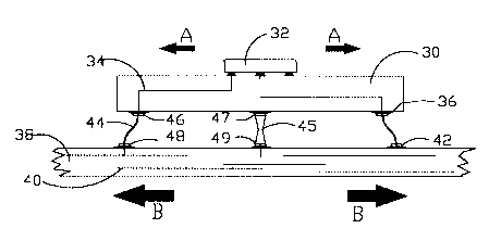
Figure 6 is a side cross-sectional view showing art IC' package according to
the present invention
assembled on a printed circuit card by conventional surface mount methods.
Assembly is
represented at an elevated coperating temperature. IC package (30) comprises
an integrated circuit
chip (32), internal conductive wiring (34) interconnecting chip (32) to a
plurality of I/O pads
(36). IC package (30) is joined to a printed circ~.iit card l 38) which
ec>mprises conductive wiring
(40), and a plurality of pads (42). Eaclc connection of package (30) to the
card (38) comprises a
flat or rectangular shaped interconnection element (44 or 4~), and a pair of
solder joints, top
solder joints (46 and 47) joining the IC package IIO pa~i (,36) to the
connecting element (44 or
45), bottom solder joints (48 and 49) joining the card pad (42) to the
connecting element (44 or
45). Arrows A represent schematically the an count and direction of thermal
deformation or
expansion of the IC package (30) duc to the efi'ects of' the operation
temperature. Arrows B
represent the amount of del:ormation and expansion of the printed circuit card
(42) resulting from
the effects of a temperature change. Arrows B ate larger than arrows A,
indicating that in this
illustrative example, circuit card ( 38) has a higher amount of thermal
expansion than the package
CA9-1999-0032 10
CA 02288605 1999-11-08
(30), thereby causing deformation of interconnection elements (44) located in
peripheral regions
of the package. However, because of the specific shape and orientation of
interconnection
elements (44) (as previously described with respect to Figures 4 and 5), the
deformation in the
elements (44) is in the direction perpendicular to thickness of the element
and not its width, and
thereby the stress in the solder joints (46 and 48) are maintained to a
relatively low level not
resulting in permanent damage to the package.
As the neutral point of the IC package (30) is approached from positions
towards the outside
edges or periphery of package (30), the amount of thermally induced
deformation becomes
smaller and smaller. Consequently, for the more central area of package (30),
it may be that it is
not essential to overcome the adverse affects of differences in thermal
expansion to have the
leads face the center of the module, but the leads could be oriented and
arranged in any manner
with respect to the neutral point without appreciable decrease in reliability
resulting from the
thermally induced deformation.
In order to achieve these goals, it is seen from the above that the shape of
the connection
elements is important. The material composition of the connecting elements is
also significant.
Leads must be made of a material with suitable compliance. It is also
advantageous to use a lead
material that has a thermal expansion coefficient that is similar to that of
the package to which
the lead is attached. Typically leads comprised of alloys of nickel and iron
or nickel, iron and
cobalt provide sufficient compliance. In particular, if the IC package is a
ceramic package, leads
made of an alloy of 42% nickel, 58% iron has been found to be appropriate.
Another material
found appropriate for leads for ceramic packages is an alloy of 54% iron, 29%
nickel and 17%
cobalt, commercially known as Kovar.
The rectangular shaped connection elements as shown in Figure 6 can be
constructed from sheet
metal using conventional stamping or other well known methods. Appropriate
surface finishes
can be applied to the connecting elements using standard plating or inlay
cladding methods.
CA9-1999-0032 11
CA 02288605 1999-11-08
One preferred way of fabricating the leads is to stamp the appropriate shape
from a flat metal
sheet, and then fold it, for example, partially upon itself, into an
appropriate form as shown in
Figure 7. Illustrated element (50) comprises a flat, rectangular shaped arm
(52), and a flat pad
(54). The width dimension of flat arm(52) is shown as being greater than the
thickness
dimension. As can be seen from Figure 7, the width of the flat arm (52) need
not be constant
throughout its length as it can be narrower at the middle, thereby offering
optimal thermal stress
distribution. This results in minimum reaction force by the connecting element
resulting from
thermal expansion and consequently minimum stress to the joint. Lead (50) of a
shape as shown
in Figure 7 also has the advantage of vertical and horizontal symmetry in that
the projection of
flat rectangular arm (52) intersects the flat pad portion (54) in its center
such that the width of the
contact pad portion (54) on both sides of the projection of the central
portion of flat arm (52) is
similar. Thus it is seen that each lead is configured such that the projection
of the substantially
flat rectangular cross-section portion of each lead intersects the contact
portion of that lead such
that the intersection is symmetrical on the contact portion.
Flat arm (52) of the element (50) of Figure 7 has a straight vertical shape
for connecting to the
solder joint of the printed circuit card. The lead (50) could thus have an end
portion that has a
wider dimension than the remainder of the flat lead. With this shape, solder
fillet solidifies with
a meniscus shape, that has no sharp angle, thereby avoiding any stress
concentration zone in the
connections to the printed circuit card. .
In another embodiment, leads can also have an additional bend near the bottom
tip of the flat
arm, to provide a second flat contact pad, that can be used to facilitate the
assembly of the
package on the printed circuit card. Other variations from the embodiment of
Figure 7 are
possible while still obtaining the advantages cited above. For example, flat
arm can be curved in
a plane perpendicular to the flat portion. Flat arm can also be at an angle
from the vertical, this
CA9-1999-0032 12
CA 02288605 1999-11-08
way some pitch variation can be obtained and card pad array can be slightly
less dense than the
corresponding IC package pad array.
The described interconnection system could also be used to interconnect two
different printed
S circuit board assemblies together. First printed circuit assembly could
have, on its surface, any
combination of prepackaged integrated circuits, bare semiconductor dies, or
discrete components.
This first printed circuit board comprises of an array of metallized pads,
onto which a plurality of
leads as described is attached in the same array configuration. Then, the
first circuit assembly can
be interconnected to a second printed circuit board assembly, using the array
of connecting
devices as described and appropriate surface mount assembly method.
The above Figures of the drawings and accompanying description are provided
for illustrative
purposes only of preferred embodiments of the invention. The invention is not
intended to be
limited to the exact shape, number of pads or connection elements or the
nature of materials
shown or described, as variations in the shown and described aspects of the
invention would be
apparent to those skilled in the art. It will be appreciated by those skilled
in the art that the
present invention can be embodied in forms other than the specific forms
provided herein
without departing from the spirit or scope of the present invention.
CA9-1999-0032 13