Note : Les descriptions sont présentées dans la langue officielle dans laquelle elles ont été soumises.
CA 02289140 1999-11-08
RF-4522 US/BERG2442 PATENT
EM405879573US
TITLE OF THE INVENTION
Angled Coaxial Connector Module
FIELD OF THE INVENTION
The present invention relates to an angled coaxial connector module for
mounting to a circuit board. More particularly, the invention relates to such
an angled coaxial
connector module which demonstrates relatively high electrical efficiency and
which can be
manufactured at relatively low cost.
BACKGROUND OF THE INVENTION
Coaxial connector modules are known in the prior art, as shown for example
by U.S. Patent No. 5,169,343. As seen in such patent, coaxial connector
modules are
employed to electrically connect high frequency signals to a circuit on a
circuit board.
However, prior art coaxial connector modules includes contact elements with
multiple
internal connections within a housing. Such internal connections resulted'in
decreased
electrical efficiency, increased parasitic effects, and increased construction
costs. These prior
devices also included relatively complex housing constructions in order to
separately channel
multiple high frequency signals and shields, thereby resulting in increased
construction and
materials costs.
Specifically, in the aforementioned U.S. Patent No. 5,169,343, within the
housing, the center contact of each contact element includes two pieces, each
inserted from a
CA 02289140 1999-11-08
RF-4522 USBERG2442 - 2 - PATENT
respective housing face into a channel, where the two pieces are soldered or
welded together
inside the housing, and where the channel is then filled with an insulating
material. As can be
appreciated, such an insertion and assembly process can be cumbersome and
prone to error.
Moreover, the quality of the joint between the two pieces can be suspect,
resulting in
electrical inefficiencies that can include unwanted resistive, capacitive,
and/or inductive
characteristics that might interfere with high frequency signals. As seen in
the same patent,
the housing includes a block of metal surrounding the insulation and acting as
a shield. The
use of a block of metal necessarily includes considerable time and expense in
milling and
drilling to form the required channels therein.
Accordingly, a need still exists for an angled coaxial connector module with
contact elements that do not have internal connections that would decrease
electrical
efficiency. Also, a need exists for such a connector module which is
constructed in a cost-
effective manner from relatively inexpensive materials such that a relatively
high state
electrical efficiency is maintained.
SUMMARY OF THE INVENTION
The present invention satisfies the aforementioned needs by providing an
angled coaxial connector module for being mounted to a circuit board. The
connector
module has a housing with a contact side for mating with a corresponding
connector and a
connecting side for mounting the connector module to the circuit board. The
housing is
constructed of an electrically insulating material.
At least one electrical contact element extends through the housing between
the contact side and the connecting side. The contact element has an
electrically conductive
CA 02289140 1999-11-08
RF-4522 USBERG2442 - 3 - PATENT
inner center contact, an electrically conductive outer shielding tube
surrounding the inner
center contact at least within the housing, and an insulating member
surrounding the inner
center contact at least within the housing and electrically isolating the
inner center contact
and the outer shielding tube. The inner center contact and the outer shielding
tube each have
a corresponding bent portion within the housing such that the contact side of
the housing is at
an angle with respect to the connecting side of the housing.
BRIEF DESCRIPTION OF THE DRAWINGS
The foregoing summary, as well as the following detailed description of
i
preferred embodiments of the present invention, will be better understood when
read in
conjunction with the appended drawings. For the purpose of illustrating the
invention, there
are shown in the drawings embodiments which are presently preferred. It should
be
understood, however, that the invention is not limited to the precise
arrangements and
instrumentalities shown. In the drawings:
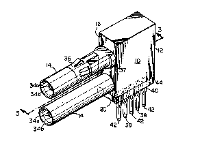
Fig. 1 is a perspective view of an angled coaxial connector module constructed
in accordance with a preferred embodiment of the present invention;
Fig. 2A is a side view of the connector module of Fig. 1, and shows such
module in relation to a receptacle connected to a circuit board, and also to a
mating connector
module mated to another circuit board;
Fig. 2B is a side view of an alternate embodiment of the connector module
shown in Fig. 2A; and
Fig. 3A and 3B are, respectively, cross-sectional views of the connector
modules shown in Figs. 2A and 2B, taken along the line 3-3 of Fig. 1.
CA 02289140 1999-11-08
RF-4522 USBERG2442 - 4 - PATENT
DETAILED DESCRIPTION OF PREFERRED EMBODIMENTS
Certain terminology may be used in the following description for convenience
only and is not considered to be limiting. The words 'left', 'right', 'upper',
and 'lower'
designate directions in the drawings to which reference is made. Similarly,
the words
'inwardly' and 'outwardly' are directions toward and away from, respectively,
the geometric
center of the referenced object. The terminology includes the words above
specifically
mentioned, derivatives thereof, and words of similar import.
Referring to the drawings in detail wherein like numerals are used to indicate
like elements throughout, there is shown in Fig. 1 an angled coaxial connector
module 10 in
accordance with a preferred embodiment of the present invention. As seen in
Fig. 1, the
connector module has a housing 12 and at least one electrical contact element
14 (two are
shown). The housing 12 has a contact side 16 for mating connector module 10
with a
corresponding connector 18 and a connecting side 20 for mounting connector
module 10 to a
printed circuit board 22 (shown in Figs. 2A and 2B). Preferably, the housing
12 is
constructed of an electrically insulating material such as a plastic or
elastomeric material. It
is noted that other electrical insulating materials may be employed without
departing from the
spirit and scope of the present invention.
As seen in the drawings, the connector module 10 has two electrical contact
elements
14. It is noted that any other number of electrical contact elements 14 may be
employed in
the connector module 10 without departing from the spirit and scope of the
present invention.
Of course, physical constraints incumbent in the dimensions of any given
housing 12 and
contact element 14 will as a practical matter limit the number of such contact
elements 14
that will fit into such housing 12. Preferably, if the connector module 10 has
a plurality of
CA 02289140 1999-11-08
RF-4522 US/BERG-2442 - 5 - PATENT
electrical contact elements 14, such elements 14 are arranged in rows and
columns on the
contact side 18 of the housing. For example, and as particularly seen in Fig.
1, the connector
module 10 shown has a pair of electrical contact elements 14 arranged in one
column and two
rows. However, most any arrangement of contact elements 14 may be employed
without
departing from the spirit and scope of the present invention. For example, the
contact
elements 14 may be arranged in staggered rows.
Referring now to Figs. 3A and 3B, each contact element 14 is shown to extend
through the housing 12 between the contact side 16 and the connecting side 20.
Preferably,
and as shown, the contact elements 14 extend through the housing 12 to the
connecting side
20 while maintaining the aforementioned row and column arrangement, although
other
internal arrangements may be employed without departing from the spirit and
scope of the
present invention. Each contact element 14 has an electrically conductive
inner center
contact 24 and an electrically conductive outer shielding tube 26 surrounding
the inner center
contact 24 at least within the housing 12. Preferably, each of the inner
center contact 24 and
the outer shielding tube 26 is formed as a substantially unitary body (i.e.,
as one piece). For
example, each element 24, 26 may be molded, or may be appropriately rolled
from a sheet of
material. As was noted above, by avoiding multiple interconnected piece,
resulting
electrical inefficiencies are avoided. Such electrical inefficiencies include
unwanted resistive,
capacitive, and/or inductive characteristics that might interfere with high
frequency signals.
Preferably, each of the inner center contact 24 and the outer shielding tube
26 is constructed
of trial or another similar electrically conductive material. However, other
electrically
conductive materials may be employed without departing from the spirit and
scope of the
present invention.
CA 02289140 1999-11-08
RF-4522 USBERG-2442 - 6 - PATENT
Preferably, each contact element 14 also includes an insulating member 28
that surrounds the inner center contact 24 at least within the housing 12 and
that electrically
isolates the inner center contact 24 and the outer shielding tube 26.
Preferably, the insulating
member 28 is constructed of PTFE (i.e., TEFLOl~ or another similar plastic or
elastomeric
material, although other insulating materials may be employed in connection
with the
insulating member 28 without departing from the spirit and scope of the
present invention.
As best shown in Figs. 3A and 3B, to allow the contact side 16 of the housing
12 to be at an angle with respect to the connecting side 18 thereof, while at
the same time
avoiding constructing each of the inner center contact 24 and the outer
shielding tube 26 of
multiple parts, it is preferable that each of the inner center contact 24 and
the outer shielding
tube 26 have corresponding bent portions 30 within the housing 12. Preferably,
and as
shown, the contact side 16 of the housing 14 is at a substantially right angle
with respect to
the connecting side 20 of the housing side 14. Accordingly, and as seen in
Figs. 2A and 2B,
the right angle connector module 10 may be mounted on the circuit board 22 and
coupled
with the corresponding right angle connector 18, with the net result being
that the circuit
board 22 and circuit board 23 occupy substantially parallel planes. However,
it may be
desirable that the circuit boards 22 and 23 not occupy parallel planes. More
generally, the
contact side 16 of the housing 14 may be at practically any angle with respect
to the
connecting side 20 of the housing side 14 without departing from the spirit
and scope of the
present invention.
Preferably, each contact element 14 is constructed to be a substantially
linear
(i.e., straight), then is bent in an appropriate area by an appropriate
mechanical device or
assembly, and then is incorporated within or molded within the connector
module 10. Such
CA 02289140 1999-11-08
RF-4522 US/BERG2442 - 7 - PATENT
appropriate bending device or assembly is known, and therefore need not be
further described
here.
Preferably, and as seen in Figs. 3A and 3B, the insulating member 28
comprises a series of discrete insulating beads 32, at least within the
housing 12, where each
bead 32 is relatively flexible. As shown, the beads 32 are necessarily
positioned within the
outer shielding tube 26 and surrounding the inner center contact 24.
Preferably, each bead
has a relatively short axial length as compared with the length of the contact
element 14.
Each insulating bead 32 is appropriately positioned adjacent neighboring
insulating beads 32
such that electrical isolation between the inner center contact 24 and the
outer shielding tube
26 is maintained, even at the bent portions 30. Importantly, the flexibility
of the insulating
beads 32, especially in the vicinity of the bent portion 30, should prevent
bead disintegration
that could potentially occur as a result of bending the electrical contact
element 14 including
the beads 32.
As best seen in Figs. 3A and 3B, each contact element 14, including the inner
center contact 24, the insulating member 28, and the outer shielding tube 26,
preferably
extends outside the housing 12 from the contact side 16 a predetermined
distance which is
appropriate for interconnection to the corresponding connector 18 (as seen
Fig. 2A). As seen,
at the extension from the contact side 16, each inner center contact 24
terminates in a female
member 34a surrounded by an insulating collar 33, and each outer shielding
tube 26
terminates at a female member 34b coaxial with and exterior to the female
member 34a and
the collar 33. Accordingly, a corresponding male-male termination 35 on the
corresponding
connector 18 (Fig. 2A) can be received by each electrical contact element 14
of the connector
module 10. However, each electrical contact element 14 may terminate at the
extension from
CA 02289140 1999-11-08
RF-4522 USBERG2442 - 8 - PATENT
the contact side 16 in any appropriate manner without departing from the
spirit and scope of
the present invention.
Owing to the dimensions of each termination 35 on the corresponding
connector 18, it may be necessary that the outer shielding tube 26 of each
contact element 14
have a relatively large first cross-sectional diameter D 1 at the extension
from the contact side
16 outside the housing 12, as illustrated in Figs. 3B. However, such
relatively large diameter
D 1 may not be necessary and may in fact be too large inside the housing 12.
In such case, it
is preferable that the outer shielding tube 26 have a relatively small second
cross-sectional
diameter D2 inside the housing 12, as also illustrated in Fig. 3B. The
relative diameters D1,
i
D2 of the outer shielding tube 26 both inside and outside the housing 12, can
and will vary.
If desired, the connector module 10 may also include a retention clip 36 to
retain the connector module 10 in a coupled relationship with the
corresponding connector 18
(Fig. 2A). Preferably, and as best seen in Fig. 1, the retention clip 36 is
positioned or formed
on the outer shielding tube 26 of one of the contact elements 14 outside the
housing 12.
Retention clip 36 includes a springed tab or the like that securely
retainingly engages a
receiving recess (not shown) in the corresponding connector 18 to lock the
connector module
10 in a mated position therewith.
Preferably, the corresponding connector 18 includes a shroud extending out
from the main body thereof (not shown) to form a cavity within which the
terminations 35
reside. The previously mentioned receiving recess is formed in such shroud.
The shroud
may also have various other slots, apertures, etc. (not shown) for receiving
corresponding
projections, keys, etc. associated with the connector module 10. One such key
37 can be seen
in the drawings as a shaped radial extension on one of the outer shielding
tubes 26 adjacent
CA 02289140 1999-11-08
RF-4522 USBERG-2442 - 9 - PATENT
the contact side 16 of the housing 12. As should be understood, then, the
connector module
and the corresponding connector 18 would form a matched set based on such
projections,
keys, apertures, slots, etc.
Referring to Figs. 3A and 3B now, the housing 12 is preferably formed by pre-
5 positioning each contact element 14 and then molding the housing material
(e.g., plastic) over
the pre-positioned elements to form a plastic over-molded housing 12. The
plastic over-
molded housing 12 provides structural support to the contact elements 14.
Methods for
performing plastic over-molding are known and therefore need not be further
described here.
Preferably, the molded plastic that forms the housing 12 has an appropriate
dielectric constant
i
10 such that stray capacitive coupling between each of the contact elements 14
is minimized,
thereby minimizing cross-talk between the contact elements 14.
Referring specifically to Fig. 3A, it is seen that in the preferred embodiment
of
the present invention, a first releasable insertion pin 38 is electrically
coupled to the inner
center contact 24 of each contact element 14 at the connecting side 20 of the
housing 12. As
seen, the first pin 38 preferably extends coaxially from the inner center
contact 24 outside the
housing 12 a predetermined distance. Such first pin 38 can either be
releasably coupled to a
complimentary pin-receiving receptacle block or pin receiver 40 (shown i'n
Fig. 2A) or
inserted into pre-formed bores in a circuit board. Preferably, and as should
be understood, the
pin receiver 40 is securely mounted to the circuit board 22. Thus, the
connector module 10
and each inner center contact 24 thereof can be releasably electrically and
mechanically
coupled to the circuit board 22 by way of each first pin 38.
Like each inner center contact 24, each outer shielding tube 26 should also be
releasably electrically coupled to circuit board 22.. It is preferable that at
least one second
CA 02289140 1999-11-08
RF-4522 USIBERG2442 -10 - PATENT
insertion pin 42 be electrically coupled to the outer shielding tube 26 of
each contact element
14 at the connecting side 20 of the housing 12. As with each first pin 38,
each second pin 42
also extends from the housing 12 a predetermined distance such that each
second pin 42 can
be releasably coupled to either pin receiver 40 or inserted into bores formed
in a circuit board.
The connector module 10 has a shield plate 44 positioned on the connecting
side 20 of the housing 12. Preferably, shield plate 44 is mechanically coupled
to the housing
12 during the aforementioned plastic over-molding of the housing 12. As best
seen in Figs.
3A and 3B, the shield plate 44 abuts and is electrically coupled to the outer
shielding tube 26
of each contact element 14. Thus, the outer shielding tube 26 of each contact
element 14 is
electrically coupled to one another by way of the shield plate 44. Preferably,
the shield plate
includes apertures through which each first pin 38 may be inserted and coupled
to a
respective inner center contact 24. The shielding plate 44 should not violate
the electrical
isolation of each inner center contact 24 and any outer shielding tube 26.
With the shield plate 44, it is preferable that each second pin 42 be
electrically
coupled to the shield plate 44. Since the outer shielding tubes 26 are
electrically coupled to
one another by way of the shield plate 44, the number of second pins 42 need
not necessarily
correspond to the number of contact elements 14. Instead, and as is shown in
Figs. 1, 2A, and
3A the number of second pins 42 may differ. The exact number of second pins 42
employed
will vary based upon many considerations, all without departing from the
spirit and scope of
the present invention.
As shown in Fig. 3A, each first pin 38 is a separate element from its
corresponding inner center contact 24, and is therefore mechanically coupled
thereto.
Likewise, each second pin 42 is a separate element from the shield plate 44,
and is therefore
CA 02289140 1999-11-08
RF-4522 USBERG2442 -11 - PATENT
mechanically coupled thereto by any suitable means. Preferably, the mechanical
coupling is
achieved by micro-butt-welding such that unwanted resistance, capacitance,
inductance, and
other electrical characteristics are avoided or at least minimized. Each first
pin 38 and its
corresponding inner center contact 24 may be formed as a substantially unitary
body, and
second pins 42 and shield plate 44 may likewise be formed as a substantially
unitary body,
without departing from the spirit and scope of the present invention. As
shown, each of the
first and second insertion pins 38, 42 includes an expanded mid-portion 46 in
order to
maintain a tight interference fit when the pin is inserted in either receiver
40 or bores in a
circuit board. However, the particular design and construction of the first
and second
I
insertion pins 38, 42 may differ without departing from the spirit and scope
of the present
invention.
Referring now Fig. 3B, it is seen that in an alternate embodiment of the
present invention, the first pins 38, have been replaced by extending the
inner center contact
24 of each contact element 14 extends outside the housing 12 from the
connecting side 20 a
predetermined distance. The connector module 10 is secured directly to the
circuit board 22
by the extension of each inner center contact 24 by any appropriate means such
as soldering.
Preferably, and as also seen Fig. 3B, pins 48 are electrically coupled to the
shield plate 44 and
extend in substantially the same direction and distance as the extensions of
the inner center
contacts 24 from the housing 12. Pins 48 can also be employed to secure the
connector
module 10 directly to circuit board 22. Preferably, the pins 48 are micro-butt-
welded to the
shield plate 44. Pins 48 and the shield plate 44 may also be formed as a
substantially unitary
body, without departing from the spirit and scope of the present invention.
CA 02289140 1999-11-08
.,
RF-4522 USBERG-2442 -12 - PATENT
In the foregoing description, it can be seen that the present invention
comprises a new and useful angled coaxial connector module. The contact
elements of the
connector module do not have internal connections that would decrease
electrical efficiency.
Also, the connector module may be constructed in a cost-effective manner from
relatively
inexpensive materials such that a relatively high state electrical efficiency
is maintained.
Changes could be made to the embodiments described above without departing
from the
broad inventive concepts thereof. It is understood, therefore, that this
invention is not limited
to the particular embodiments disclosed, but it is intended to cover
modifications within the
spirit and scope of the present invention as defined by the appended claims.