Note : Les descriptions sont présentées dans la langue officielle dans laquelle elles ont été soumises.
CA 02290817 1999-11-19
WO 98/52876 PCTIAU98/00364
1
REMOVAL OF CELL GROWTH FROM A BODY OF WATER
TECHNICAL FIELD
This invention relates to a method and apparatus for the cleansing of
bodies of water such as swimming pools, reservoirs, dams and the like. In
particular, it is directed to the removal of bacteria, microbes and other cell
growth from water.
BACKGROUND ART
Large bodies of water such as swimming pools, water catchment areas
and similar where the water therein is to be in subsequent contact with people
(either by swimming or bathing in the body of water, or by drinking the water)
requires cleansing. Although various filters incorporating a filtration medium
such as sand can be used to remove particulate matter and other solid debris,
the removal of harmful bacteria and other microbiological growth is more
difficult. Such bacteria and the like are usually removed by regularly dosing
the body of water with a suitable chemical. For example, sodium hypochlorite
is commonly added to swimming pools to maintain the dissolved chlorine
content of the water at a level which is lethal to any bacteria and the like
which
is present in the water. In municipal works, where a body of water has to be
purified to drinking water standards, a large range of chemicals may be added
2 o to the water to purify it.
There are a number of disadvantages to these existing methods.
Swimming pools usually cannot be used until some period after treatment
because the chlorine content necessary to purify the water often irritates the
eyes of any person in the pool. In drinking water treatment, there is
increasing
2 5 concern by the community that the deliberate addition of chemicals into
the
water supply is harmful in itself. For example, it can lead to allergic
reactions in
some consumers of the treated water. Therefore, for an increasing number of
consumers, it is necessary to filter or otherwise further treat the supplied
water
before it can be used or consumed. Of course, the use of chemicals andlor
3 o further treatment of supplied water all add to the financial costs of
maintaining
an acceptable supply of water for use by the community.
It is thus a general object of the present invention to overcome, or at
SUBSTITUTE SHEET (RULE 26)
CA 02290817 1999-11-19
WO 98152876 PCT/AU98100364
2
least ameliorate, one or more of the above disadvantages.
DISCLOSURE OF INVENTION
According to the present invention there is provided a method of for the
removal of bacteria, microbes and other cell growth from a body of water, said
method comprising:
applying an electro-magnetic field to a section of said pipe or similar
conduit communicable with the body of water as water passes therethrough,
said electro-magnetic field having a frequency or a range of frequencies
sufficient to inhibit or remove said bacteria, microbes or other cell growth
from
l0 said water.
The application of the electro magnetic field to said section of pipe can
be achieved by magnetizing an element or elements positioned on the wall of
the pipe or conduit.
Four equally spaced elements can be placed on the wall of the pipe or
conduit.
The elements can be elongate strips of ferrite material.
The ferrite material can be manganese-zinc.
The element can be a magnetizable coil.
According to a further aspect of the present invention there is provided
2 o apparatus for the removal of bacteria, microbes and other cell growth from
a
body of water, said apparatus comprising:
a magnetizable element adapted to be disposed about a section of a
pipe communicable with the body of water;
means for applying a signal to said magnetizable element to create an electro-
2 5 magnetic field within said pipe, said electro-magnetic field having a
frequency
or a range of frequencies sufficient to inhibit or remove said bacteria,
microbes
or other cell growth from said water.
The magnetizable element can comprise one or more ferrite elements
placed on the wall of the section of pipe.
3 o The one or more ferrite elements can be manganese-zinc elements.
The magnetizable element can be a coil for application of the
electromagnetic field to the pipe or conduit the coil being wound about a
SUBSTITUTE SHEET (RULE 26)
CA 02290817 1999-11-19
WO 98/52876 PCT/AU98/00364
3
polyvinyl chloride (PVC) or other non-ferrous former which is located
coaxially
about the pipe or conduit.
An AC voltage can be applied to the magnetizable element to generate
the electro-magnetic field.
The voltage can be 5 volts AC.
The frequency of the voltage applied to the magnetizable element can
vary to sweep a range of frequencies in the range of 2 KHz to 7KHz.
The signal applied to the magnetizable element can be in the form of a
positive going square wave followed by a negative going spike having a
variable frequency.
The means for generating the signal can comprise first and second
square wave oscillators whereby the output of the second oscillator is
modulated in frequency by the output of the first oscillator.
The signal generating means can include a third square wave oscillator
whereby the output of the second oscillator is used to frequency modulate the
output of the third square wave oscillator.
Amplifier means can be employed for amplifying the output of the third
square wave oscillator, the output of the amplifier means is adapted to be
connected to the magnetizable element via capacitance means to defne the
2 o required form of the signal.
BRIEF DESCRIPTION OF THE DRAWINGS
In order that the invention may be more readily understood and put into
practical effect, reference will now be made to the accompanying drawings
which illustrate a preferred embodiment of the invention and wherein:
Figure 1 illustrates the general nature of the apparatus constructed
according to the present invention;
Figure 2 is a circuit diagram of the circuit for generating and applying a
signal to a pipe with water flowing therethrough; and
Figure 3 illustrates the appiication of the apparatus of the invention to a
3 o swimming pool.
Figure 4 is a circuit diagram of an alternative circuit for generating and
applying a signal to a pipe with water flowing therethrough, and
SUBSTITUTE SHEET (RULE 26~
CA 02290817 1999-11-19
WO 98/52876 PCT/AU98/00364
4
Figure 5 is a view of a section of pipe from a swimming pool filtration
system having apparatus according to the present invention attached thereto,
and
Figure fi is a cross-sectional view of a pipe of a swimming pool
installation having probes of the present invention positioned thereon, and
Figure 7 is a perspective view of the pipe band in accordance with
another aspect of the present invention.
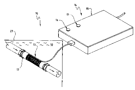
Referring firstly to Figure 1, there is illustrated an apparatus 10
comprising a former 12 manufactured from a non-magnetic non-ferrous
l0 material such as a plastics material and preferably a polyvinyl chloride
(PVC).
Wound about the former 12 are a plurality of turns of wire forming to a coil
13
which is connected to receive a signal from a signal generator 14.
The former 12 is preferably 40 mm in diameter having wound thereon
three layers of 0.315 mm insulated copper wire extending approximately 170
mm along the former 12. The former 12 may be provided with an outer casing
to surround the windings or the layers of wire may be provided with a shrink
sleeving.
The coil is adapted to be connected to a signal generator is housed
within a casing 15 provided with an indicator 16 in the form of a light
emitting
2 o diode (LED) which indicates circuit operation and a further indicator 17
in the
form of a light emitting diode (LED) which indicates power supply to the
apparatus 10. Mounted within the casing 15 is a circuit board 9 8 which
carries
the components of the signal generating circuit 19 and associated power
supply 20.
The power supply 20 includes a bridge rectifier B1 and capacitator C1
which are arranged to be connected to an AC supply 21 to provide a pulsating
DC voltage at the output of the rectifier B1 at a frequency in this embodiment
of
100 Hz which is then applied to a capacitator C2 which filters and smooths to
supply a DC voltage. This smoothed DC voltage is then applied to a regulator
3o Reg1 which outputs a fixed DC voltage in this instance 12 volts which in
conjunction with capacitator C3 provides a regulated 12 volt supply. Resistor
R2 applies the voltage output from the bridge B1 to the externally mounted LED
SUBSTITUTE SHEET (RULE 26)
CA 02290817 1999-11-19
WO 98/52876 PCTIAU98/00364
1fi which indicates that power is supplied to the circuit. The resistor R2
limits
the current flowing to the LED 16.
The resistor R4, Zener diode Z1 and capacitor C4 form a further power
supply (VCC), preferably a 5 volts DC supply, to be applied to the signal
5 generator circuit 19. Alternatively, a further regulator may be used to
supply a
regulated output for supply to the circuit 19.
The signal generating circuit 19 is primarily formed about a quad and
gate Schmitt trigger which in this embodiment comprise a type 4093 CMOS
Integrated Circuit U1 which has four separate gates designated U1:A, U1:B,
1o U1:C and U1:D. The gates U1:B, U1:C and U1:D are used as oscillators as
described below.
The gate U1:C forms an oscillator 22 with resistor R13 and capacitator
C11 whose normal frequency of oscillation as determined by resistor R13 and
capacitator C11 is 10 Hz. The gate U1:D is configured as an oscillator 23 with
resistor R16 and capacitator C13 which set the normal frequency of oscillation
at 7 KHz. Both oscillators 22 and 23 provide a positive going square wave
output. The output of the oscillator 23 is connected to the input of the
oscillator
22 though resistors R13 and R14 and capacitor C12 which is charged and
discharged by the output of the oscillator 23 to apply a modulating signal to
the
input of the oscillator 22. The output of the oscillator 22 is thus a
modulated
positive going square wave of the form illustrated schematically at 24 where
frequency varies as determined by the output of the oscillator 23. The average
frequency of this output signal is 3.8 KHz.
This output signal is applied via resistor R12 to the base of a transistor
2 5 Q4 and the varying frequency of the signal 24 serves to switch transistor
Q4 on
and off at the varying frequency. The purpose of R12 is to limit the current
to
the base of transistor Q4.
The gate U1:B in is connected with resistor R10 and capacitors C9 and
C10 to form a further oscillator 25 whose output is normally a positive going
3 o square wave. As with the oscillators 22 and 23, the frequency of this
oscillator
is controlled by the values of its associates resistor and capacitor in this
case
resistor R10 and capacitors C9 and C10. The oscillator 25 would normally run
SUBSTITUTE SHEET (RULE 26)
ICAI 02290817 1999-11-19
WO 98152876 PCT/AU98/00364
6
at a frequency of 2.6 KHz. The capacitors C9 and C10 are connected in series
and are of the same value so that the capacitance of the series capacitors C9
and C10 is half the total capacitance of the capacitors. This oscillator 25 is
modulated by the output signal 24 of the oscillator 22 applied through the
transistor Q4. The capacitors C9 and C10 are connected to the collector of the
transistor Q4 which when switched on and off the shunts the capacitor C9 to
ground at a frequencies determined by the variable frequencies of the output
signal 24. The effect of this switching is to double the capacitance of the
series
capacitors C9 and C10 every time the transistor Q4 is switch on. This
therefore
halves the output frequency at output of the oscillator 25.
The output of the oscillator 25 is connected via an R-C circuit formed
by resistor R9 and capacitator C8 to a Darlington pair of transistors Q3 and
Q2
which amplify the signal and apply the amplified signal to the positive plate
of a
capacitor C6. The capacitor C6 isolates DC voltages at the more negative
plate and applies the signal to the coil 13 via a connector J2. When the coil
13
is connected, the signal passes through the coil 13 and returns to the ground
via resistor R7. The signal applied to the coil 13 as indicated at 26
comprises a
positive going square wave and a negative spike which returns through an
exponential curve to zero.
2 0 The fourth gate U 1:A of the integrated circuit U 1, is used as a detector
to show that the coil 13 is operating. Resistors R5 and R11 form a voltage
divider connected to the voltage VCC and applying an input to the gate U1:A.
The input of the gate U1:A is also connected via capacitor C5 and resistor R6
to the coil 13.
2 5 When the coil 13 is not connected or operating the voltage applied by
the voltage divider R5 and R11 to the input of the gate U1:A causes the output
of the gate U1:A to be low. When the coil 13 is operating, the input voltage
to
the gate U1:A is lowered by capacitor C5 AC coupling this voltage to R6. When
the input voltage goes below the trip point of the Schmitt trigger U 1:A, the
30 output of the gate U1:A goes high thus supplying a voltage to resistor R3
which
is connected to the base of transistor Q1 and serves to limit the current to
the
transistor Q1. When this current limited voltage is applied to the transistor
Q1
SUBSTITUTE SHEET (RULE 26)
r. _ _._. __~_.__.r....-.__._.~_ _ _ _ __
CA 02290817 1999-11-19
WO 98/52876 PCT/AU98100364
7
and current limiting resistor R1 and thus is illuminated when the coil 13 is
connected and operating. Thus LED 17 serves as a coil operating indicator.
llVhen the coil 13 is removed or not operating the transistor Q1 is
witched off due to an absence of base current and the LED 17 goes out. Both
LED 16 and LED 17 are preferably connected externally through connector J3.
The output to the coil connector or jack J2 comprises a jumble or range
of frequencies generated by the gated U1:C and U1:D. As stated above both
U1:C and U1:D are connected as separate oscillators with the output of U1:D
being applied to the input of U1:C. The oscillator 22 including gate U1:C
l0 provides substantially higher frequency than the oscillator circuit 23
which
includes gate U1:D. Thus if disconnected from each other, the oscillator 22 of
U1:C will provide a frequency of approximately 10 Hz and that of U1:D
approximately 7 KHz. The combined circuit generates a sweep of frequencies
usually in the range of 1 KHz to 7 KHz.
It is however within the scope of the present invention to provide an
oscillator circuit which provides a single frequency output or a range of
frequencies beyond the above range for application to the coil. Appropriate
frequency selection is made in accordance with the nature of the cell growth
andlor the quality of water flowing through the pipe.
2 o In use and as shown in Figure 3, the apparatus of the invention may be
suitably applied to an installation 27 representing a swimming pool. The
former
12 carrying the coil 13 is located about the pipe 12 and is ptaced in the pool
below the surface of the water. The signal generator 14 housed in the housing
15 is mounted in any suitable location and connected to the coil 13 through
the
2 5 wires 32.
With respect to Figures 4 of the drawings, and in accordance with a
further aspect of the present invention a signal is primarily generated from a
single-ship microcontroller 22 which in this embodiment comprises a type PIC
16C73A microcontroller. The 4.00 Mhz crystal X1 and two 15pF capacitors
3o C17 and C18 form the base frequency oscillator for the microcontroller. C14
and C15 serve as by-pass capacitors that stabilize the power supply to the
microcontroller. The DS1233-10 reset unit ensures the microcontroller starts
SUBSTITUTE SHEET (RULE 26)
/CAI 02290817 1999-11-19
WO 98/52876 PCT/AU98I00364
8
successfully on every power up.
The microcontroller generates an internal square waive signal at 10 Hz
modulated at 7kHz producing a signal with an average frequency of 3.8kHz.
This signal is used to vary the frequency of a third oscillator, the third
oscillator
normally running at a frequency of 2.6 kHz. The effect of the signal applied
to
this third oscillator is that it will have the frequency of the third
oscillator every
time the signal goes high and return the third oscillator to it's normal
frequency
when the signal goes low. The output of this third oscillator RCO (CDRV) is
applied via an R0-C circuit formed by resistor R9 and capacitor C8 to a
Darlington pair of transistors Q3 and Q2 which amplify the signal to the
positive
plate of a capacitor C6. The capacitor C6 isolates DC voltages at the more
negative plate and applies the signal to the coil 13 via a connector j2. When
the coil 13 is connected, the signal passes through the coil 13 and returns to
ground via resistor R7. The signal applied to the coil 13 as indicated at 26
comprises a positive going square wave and a negative spike which returns
through an exponential curve to zero. Resistors R5 and R11 form a voltage
divider connected to the voltage VCC and applying an input to the
microcontroller at RBO (CFB). This input is also connected via capacitor C5
and resistor R6 to the coil 13 and is used as a detector to show that the coil
13
2 o is operating.
When the coil 13 is not connected or operating the voltage applied by
the voltage divider R5 and R11 to the input of the microcontroller is low and
the
microcontroller turns LED 17 off. If the coi! 13 is connected and operating
the
input voltage goes high and the microcontroller turns LED 17 on. Thus LED 17
2 5 serves as a coil operating indicator. The base frequencies for operation
are
stored in a serial Electrically Erasable Programmable Read Only Memory
(EEPROM) U5 which in this case is a PIC24C04AP. These frequencies may
be changed to suit a particular application by means of adjusting via two push-
buttons PB1 and PB2 and displays DSP1 and DSP2. These pushbuttons and
3o displays are preferably located on an additional board that is able to plug
into
the main system board, thereby limiting the ability to change frequencies to
only
those that are authorised to do so.
SUBSTITUTE SHEET (RULE 26)
CA 02290817 1999-11-19
WO 98/52876 PCTIAU98I00364
9
Transistors Q1 and Q5 serve to multiplex the display of numbers. A
number display may be applied to DSP1 only by the microcontroller turning on
Q1 and turning off Q5. To display a number on DSP2 the microcontroller turns
on Q5 and turns off Q1. By alternating this process at approximately 60 times
a
second, the human eye wilt not be able to detect any amount of flickering due
to the displays repeatedly being switched on and off.
Figures 5 to 7 of the drawings illustrates a section of piping in a
swimming pool installation to which probes of an apparatus according to
another aspect of the present invention are attached. A plurality of probes
30'
1 o having electrical connection to the output of the signal generating
apparatus of
Figure 4 are positioned on the outer surface of a suction of pipe 31'. The
probes 30' may be in the form of elongate bars of a ferrite material. Our
trials to
date have indicated that manganese-zinc supplied by NEOSID AUST. PTY
LIMITED and identified by the code F8 is a suitable material. Good results
have been achieved by using one to five probes 30'. According to data
provided by NEOSID AUST. PTY LIMITED their F8 coded ferrite material has
an optimum frequency range of between .1 and .5 MHz. A convenient manner
of attaching the probes is to enclose individual probes within equally spaced
pockets 32' of a band 33'. The band 33' can be mounted on a section of pipe
2 0 and secured using Velcro or like attachments.
The use of the method and apparatus of the present invention should
thus at least reduce the costs of maintaining a healthy water supply by means
which are both more environmental friendly and more acceptable to the general
community.
it will be appreciated that the above examples are illustrative only of the
present invention and that modifications and alterations can be made thereto
without departing from the inventive concept as hereinbefore described.
SUBSTITUTE SHEET (RULE 26)