Note : Les descriptions sont présentées dans la langue officielle dans laquelle elles ont été soumises.
CA 02291198 2002-03-07
r
1
SY~TITCHING P0V1ER SUPPLY UNIT
BACKGROUND OF THE INVENTION
1. Field of the Invention
The present invention relates to a switching power supply
unit having a main switching element and a single or a
plurality of auxiliary switching elements which perform ON/OFF
operations in synchronism with or opposite to ON/OFF
operations of the main switching element.
2 Descri t~ the Related Art
In general, in electronic equipment such as electronic
calculators and communication devices, a switching power
supply unit has been widely used for supplying a stablized DC
voltage from a commercial AC power supply. As the switching
power supply unit, there are provided switching power supply
units having different circuit systems, such as a forward
converter, or a fly-back converter, in which a main switching
element, which is connected in series to a primary winding or
a transformer, is repeatedly turned on/off to intermittently
apply an input voltage to the transformer so as to obtain a DC
output through a rectifying and smoothing circuit connected to
a secondary winding of the transformer. In contrast with
these switching power supply units, there are provided various
kinds of switching power supply units, in which improvement in
circuit characteristics can be achieved by adding a circuit
which includes an auxiliary switching element for performing
ON/OFF operations in synchronism with ON/OFF operations of a
main switching element or in reverse thereto.
A description will be given of a structure of a
conventional switching power supply unit having such an
auxiliary switching element referring to the drawings.
First, the conventional art disclosed in Japanese
Unexamined Patent Publication No. 8-317647 published November
29, 1996, will be illustrated with reference to Fig. 13.
In this figure, reference numeral 50 represents a
CA 02291198 2002-03-07
' 2
switching power supply unit, which has a partial-resonance
converter circuit 51 and a drive circuit 52. Of these
components, the partial-resonance converter circuit 51 is
composed of capacitors C51, C52, C53, and C54, diodes D51,
D52, and D53, a transformer T51, a main switching element 551,
and an auxiliary switching element 552.
In addition, the drive circuit 52 is composed of an
output control circuit 53, comparators 54 and 55, an inverter
56, an isolator circuit 57, a triangle-wave oscillator 58, a
light-emitting element Pa of a photo coupler, a light-
receiving element Pb of the photo coupler, a transitor Q51,
and resistors R51, R52, and R53.
In the switching power supply unit having the above-
described structure, the auxiliary switching element S52
performs ON/OFF operations opposite to the ON/OFF operations
of the main switching element 551.
Next, another conventional art disclosed in U.S. Patent
No. 5,519,599, issued May 21, 1996, will be illustrated with
reference to Fig. 14.
In this figure, reference numeral 60 represents a
switching power supply unit, in which an FET disposed on the
secondary side of a transformer is used for rectification.
This is generally referred to as a synchronous rectification
system. The switching power supply unit 60 is composed of a
transformer T61, an input capacitor C61, an FET Q61 as a main
switching element, an FET Q62 as an auxiliary switching
element, a choke coil L61, an output capacitor C62, a light-
emitting-side photo coupler PA, a light-receiving-side photo
coupler PB, comparators 61, 62, and 63, a triangle-wave
oscillator 64, isolation an inverter 67, a control circuit 68,
and a control-signal output circuit 69. Of these constituent
parts, the control-signal output circuit 69 is composed of
transistors Q64 and Q65, and resistors R61 to R65.
In the switching power supply unit 60 having the above-
CA 02291198 2002-03-07
3
described structure, the FET Q62 performs ON/OFF operations in
synchronism with the ON/OFF operations of the FET Q61, whereas
the FET Q63 performs ON/OFF operations in opposition to the
ON/OFF operations of the FET Q61.
In each of the above-described switching power supply
units, however, the circuit part driving the auxiliary
switching element is formed of an IC. Additionally, since a
ground level is different between the main switching element
and the auxiliary switching element, installation of an
isolation circuit composed of photoelectric elements and/or
transformers such as a pulse transformer and a photo coupler
is necessary. In this way, when an IC, a pulse transformer,
or the like is used, the circuit structure is complicated and
production cost is increased. Further, and possibly more
important such an increase in the number of parts can also
increase in size and weight.
SUI~iARY OF THE INVENTION
The present invention can solve the aforementioned
drawbacks associated with the conventional switching power
supply unit and provides a switching power supply unit capable
of reducing costs, size, and weight, by simply and easily
forming a circuit for controlling an auxiliary switching
element performing ON/OFF operations in synchronism with or in
opposition to the ON/OFF operations of a main switching
element in which an IC and an isolation circuit are not used.
The switching power supply unit according to the
invention includes a DC power supply, a transformer having a
primary winding, a main switching element for performing
ON/OFF operations and connected in series to the primary
winding, and an auxiliary switching element for performing
ON/OFF operations in synchronism with or in opposition to the
ON/OFF operations performed by the main switching element, the
auxiliary switching element having an ON time, the transformer
having an auxiliary switching element drive winding disposed
in the transformer to generate a voltage turning on and off
the
w CA 02291198 1999-11-29
- 4 -
auxiliary switching element, a first impedance circuit
including a first resistor and a first capacitor are mutually
connected in series, and a differentiating circuit for
determining the timing for turning on the auxiliary switching
element and the ON time thereof is connected to the auxiliary
switching element drive winding.
Furthermore, in the switching power supply unit of the
invention, the auxiliary switching element comprises a
transistor, the gate of which is connected to an end of the
switching element drive winding via the first capacitor, the.
source of which is connected to the other end thereof, and the
first impedance circu it is connected between the gate and the
source of the transistor.
Additionally, in this switching power supply unit, the
differentiating circuit has a second impedance circuit
connected in series to the first capacitor.
Furthermore, in the above switching power supply unit, the
second impedance circuit has one of a second resistor and an
inductor.
In the switching power supply unit of the invention, the
impedance value of one of the first and second impedance
circuits or the impedance values of both thereof vary with the
direction of current flowing through one or both of the
impedance circuits.
Furthermore, in the switching power supply unit of the
present invention, the second capacitor is connected in
parallel to the first impedance circuit.
Furthermore, in the switching power supply unit of the
present invention, the impedance value of the first impedance
circuit varies with the DC output or signals from the outside
of the first impedance circuit.
According to the switching power supply unit of the
present invention, since the auxiliary switching element is
driven by voltage generated in the auxiliary switching element
drive winding of the transformer, the use of an IC or a
CA 02291198 1999-11-29
- 5 -
photoelectric element such as a pulse transformer and a photo
coupler is not necessary, so that decrease in the number of
components, reduction in size, weight, and production cost, can
be achieved.
In addition, the second impedance circuit suppresses an
abrupt application of the voltage generated in the auxiliary
switching element drive winding, and the operation for turning
on the auxiliary switching element is thereby delayed so as to
set a dead time, in which both the main switching element and
the auxiliary switching element are turned off.
Furthermore, the ON time of the auxiliary switching
element and the dead time can be adjusted by selecting the
resistance value or the impedance value of a resistor
comprising the second impedance circuit.
Furthermore, the voltage between the gate and the source
of the auxiliary switching element is increased or decreased by
selecting the resistance value or the impedance value of an
element comprising the first impedance circuit and by selecting
the capacity of the second capacitor to adjust the ON time of
the auxiliary switching element so as to adjust the timing for
turning off the auxiliary switching element and set a dead time
in which both the main switching element and the auxiliary
switching element are turned off. In addition, with this
arrangement, the length of the dead time can be adjusted.
Furthermore, since the main switching element and the
auxiliary switching element perform mutually reversed ON/OFF
operations, with a dead time put between the operations, there
are no problems with occurrence of losses and destruction of
the elements resulting from the simultaneous turn-on of both
elements.
Furthermore, the second impedance circuit suppresses
occurrence of surge voltage between the gate and source of the
auxiliary switching element.
Additionally, the inductor comprising the second impedance
circuit permits the surge voltage between the gate and the
CA 02291198 1999-11-29
- 6 -
source of the auxiliary switching element to be reduced.
Further, the first capacitor cuts off a direct current to
reduce the drive loss of the auxiliary switching element.
Furthermore, variations in the capacitance can be
controlled to enhance reliability by setting the capacitance of
the second capacitor larger than the parasitic capacitance of
the auxiliary switching element to make the capacitance of the
second capacitor dominant.
Additionally, since the impedance value of the first
impedance circuit varies or switches according to the output. of
the switching power supply unit, the impedance value between
the gate and the source of the auxiliary switching element can
be adjusted. This permits the ON time of the auxiliary
switching element to be most appropriately adjusted according
to the output of the switching power supply unit.
In addition, since the impedance value of the first or
second impedance circuit changes according to the direction of
current flowing through the circuit, the most appropriate
impedance value can be set according to a positive voltage and
a negative voltage generated in the auxiliary switching element
drive winding or the on/off ratio of the auxiliary switching
element. Furthermore, an impedance value, in which variations
in the ON time of the auxiliary switching element are minimized
with respect to variations in the on/off ratio of the auxiliary
switching element, can be set.
For the purpose of illustrating the invention, there is
shown in the drawings several forms which are presently
preferred, it being understood, however, that the invention is
not limited to the precise arrangements and instrumentalities
shown.
BRIEF DESCRIPTION OF THE DRAWING~~
Fig. 1 is a circuit diagram illustrating the basic
structure of a switching power supply unit according to the
present invention.
CA 02291198 1999-11-29
Fig. 2 is a circuit diagram illustrating a switching power
supply unit according to a first embodiment of the present
invention.
Fig. 3 is a waveform chart showing a voltage in each part
of the switching power supply unit shown in Fig. 2.
Fig. 4 is a waveform chart showing a voltage between the
gate and the source of an auxiliary switching element
constituting the switching power supply unit shown in Fig. 2.
Fig. 5 is a waveform chart showing a voltage between the
gate and the source of another auxiliary switching element
constituting the switching power supply unit shown in Fig. 2.
Fig. 6 is a voltage waveform chart including the surge
voltage between the gate and the source of the auxiliary
switching element constituting the switching power supply unit
shown in Fig. 2.
Fig. 7 is a circuit diagram showing a modification of the
switching power supply unit shown in Fig. 2.
Fig. 8 is a circuit diagram showing another modification
of the switching power supply unit shown in Fig. 2.
Fig. 9 is a circuit diagram showing another modification
of the switching power supply unit shown in Fig. 2.
Fig. 10 is a circuit diagram showing another modification
of the switching power supply unit shown in Fig. 2.
Fig. 11 is a circuit diagram showing another modification
of the switching power supply unit shown in Fig. 2.
Fig. 12 is a circuit diagram illustrating a switching
power supply unit according to a second embodiment of the
present invention.
Fig. 13 is a circuit diagram illustrating a conventional
switching power supply unit.
Fig. 14 is a circuit diagram illustrating another
conventional switching power supply unit.
,. CA 02291198 1999-11-29
_ $
Hereinafter, the preferred embodiments of the present
invention are explained in detail with reference to the
drawings.
In Fig. 1, reference numeral 1 represents a switching
power supply unit, which is an application circuit of the one
ordinarily referred to as a fly-back converter. The switching
power supply unit 1 includes a DC power supply E, a transformer
T, a capacitor 10, a main switching element SW1, an auxiliary
switching element SW2, a main switching element control circuit
2, and a differentiating circuit 3.
The transformer T has a primary winding N1, a secondary
winding N2, a main switching element drive winding N3, and an
auxiliary switching element drive winding N4. Additionally, on
the secondary side of the transformer T is disposed a
rectifying diode D1 and a smoothing capacitor C4.
In addition, as the transformer, an inductance element
using the entire part or a part of the primary winding and the
secondary winding may be used.
The main switching element control circuit 2 uses the
voltage generated in the main switching element drive winding
N3 to control the drive of the main switching element SW1.
When the main switching element SW1 is turned on, the voltage
generated in the DC power supply E is applied to the primary
winding N1 of the transformer T so as to charge energy in the
primary winding N1. In contrast, when it is turned off, energy
discharged from the secondary winding N2 is rectified and
smoothed by the diode D1 and the capacitor C4 to supply
electrical power to a load.
The differentiating circuit 3 is composed of a first
resistor and a first capacitor connected in series to each
other. This circuit 3 uses voltage generated in the auxiliary
switching element drive winding N4 to control the drive of the
auxiliary switching element SW2 so as to alternately turn
on/off the auxiliary switching element SW2 with respect to the
main switching element SW1.
CA 02291198 1999-11-29
_ g _
Next, an embodiment of the switching power supply unit
having the above basic structure will be illustrated referring
to the drawings.
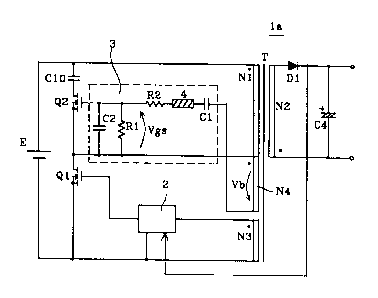
In Fig. 2, reference numeral la indicates a switching
power supply unit in accordance with a first embodiment. This
adopts an active clamp system in the application circuit of a
fly-back converter, in which a surge voltage to the main
switching element is clamped.
The switching power supply unit la has a DC power supply E
and a transformer T. The DC power supply E may be obtained by
rectifying and smoothing an AC input. In addition, the
transformer T has a primary winding N1, a secondary winding N2,
a main switching element drive winding (hereinafter referred to
as a first drive winding) N3, and an auxiliary switching
element drive winding ((hereinafter referred to as a second
drive winding) N4.
In addition, a field-effect transistor (hereinafter
referred to as an FET) Q1 as the main switching element, the
primary winding N1 of the transformer T, and the DC power
supply E are connected in series, and a field-effect transistor
(FET) Q2 as the auxiliary switching element, and a capacitor
C10 are connected between both ends of the primary winding N1
of the transformer T.
In this case, the gate of the FET Q1 is connected to an
end of the first drive winding N3 via the main switching
element control circuit (hereinafter referred to as a main
control circuit) 2, the source thereof is connected to the DC
power supply E, and the drain thereof is connected to an end of
the primary winding N1. The source of the FET Q2 is connected
to the drain of the FET Q1, the gate of the FET Q2 is connected
to an end of the second drive winding N4 of the transformer T
via the auxiliary switching element control circuit
(hereinafter referred to as an auxiliary control circuit) 3,
and the drain thereof is connected to the capacitor C10.
Furthermore, the gate and the source of the FET Q2 are
CA 02291198 1999-11-29
- 10 -
connected to the second drive winding N4 via the auxiliary
control circuit 3. In this case, the auxiliary control circuit
3 includes a resistor R1 as a first impedance circuit, a
resistor R2 and a bead 4 as a second impedance circuit, a
capacitor C1 as a first capacitor, and a capacitor C2 as a
second capacitor. Among these components, the resistors Rl and
R2, the bead 4, and the capacitor C1 are mutually connected in
series to form a differentiating circuit. In addition, the
resistor R1 is connected between the gate and the source of the
FET Q2, and the capacitor C2 is connected in parallel to the.
resistor R1.
Furthermore, the switching power supply unit la has a
diode D1 as a rectifying circuit and a capacitor C4 as a
smoothing circuit on the secondary side of the transformer T.
As the first impedance circuit, a resistance parasitically
existing inside of the FET Q2 may be used, and as the second
capacitor, a capacitance parasitically existing inside of the
FET Q2 may be used.
Next, the operation of the switching power supply unit la
having the above structure will be illustrated below.
First, on startup, voltage is applied to the gate of the
FET Q1 via a starting resistor (not shown) disposed in a main
control circuit 2, whereby the FET Q1 is turned on. As the FET
Q1 is turned on, voltage of the same polarity mutually occurs
in the primary winding N1 of the transformer T and the first
drive winding N3, whereby the FET Q1 is in the ON state so as
to charge excitation energy in the primary winding N1.
In addition, when the FET Q1 is turned off by the main
control circuit 2, excitation energy charged in the primary
winding N1 of the transformer T is discharged as electric
energy via the secondary winding N2 and then rectified to be
smoothed by the diode D1 and the capacitor C4 so as to supply
power to a load.
Then, when the excitation energy charged in the primary
winding N1 of the transformer T is all discharged via the
CA 02291198 1999-11-29
- 11 -
secondary winding N2, a voltage having the same polarity as
that of the voltage generated on startup is generated so as to
turn on the FET Q1. As a result, with ON/OFF operations of the
FET Q1, electric energy is supplied to the load.
The FET Q2 performs ON/OFF operations opposite to the
ON/OFF operations of the FET Q1 to reduce the switching losses
and switching surges of the FET Q1. The operations of the FET
Q2 will be illustrated below.
First, as the FET Q1 is turned off, a voltage of the
polarity opposite to a voltage generated on startup of the FET
Q1 is generated in winding N4. This voltage Vb permits a
voltage to be applied between the gate and the source of the
FET Q2, and then, the voltage Vgs between the gate and the
source of the FET Q2 exceeds a threshold voltage Vth of the FET
Q2 to turn on the FET Q2.
Next, referring to Fig. 3, a description will be given of
the operations of the FET Q1 and FET Q2. In this figure,
reference numerals S1 and S2 schematically indicate the ON/OFF
state of the FET Q1 and FET Q2. Reference numeral Vb indicates
voltages at both ends of the second drive winding N4 of the
transformer T, and reference numeral Vgs indicates a voltage
between the gate and the source of the FET Q2.
The drive pulses S1 and S2 perform mutually-reversed
ON/OFF operations, with a dead time dtl and a dead time dt2
therebetween, in which both of them are off.
When the FET Q1 is turned on, the positive voltage Vb is
generated in the second drive winding N4 and applied to the
gate of the FET Q2. In this situation, the voltage Vgs between
the gate and the source of the FET Q2, that is, a voltage
applied between both ends of the resistor R1 comprising the
differentiating circuit makes a rapid ascent. Then, at a time
in which the voltage Vgs between the gate and the source
exceeds a threshold voltage Vth of the FET Q2, the FET Q2 is
turned on. After this, the voltage Vgs between the gate and
the source reaches a peak value. Next, with the
CA 02291198 1999-11-29
- 12 -
differentiating circuit comprising the capacitor C1 and the
resistor R1, the voltage Vgs between the gate and the source is
attenuated at a CR time constant value determined by the
capacitance value C of the capacitor C1 and the resistance
value R of the resistor R1, and again reaches the threshold
voltage Vth. This operation terminates the ON time of the FET
Q2, and when the FET Q1 is next turned on, the polarity of the
voltage Vb is reversed.
Then, when the FET Q1 is turned off again, the positive
voltage Vb is generated in the second drive winding N4 and
applied to the gate of the FET Q2 so as to increase the voltage
Vgs between the gate and the source, and furthermore the
changes described above are repeated. As a result, the time
that takes the voltage Vgs between the gate and the source
after exceeding the threshold voltage Vth of the FET Q2 to
reach the threshold voltage Vth by attenuation due to the CR
time constant of the differentiating circuit is equivalent to
the ON time of the drive pulse S2 of the FET Q2.
Furthermore, since the resistor R2 and the bead 4
comprising the second impedance circuit permits an abrupt
application of the voltage Vb between both ends of the resistor
R1 to be suppressed, rising of the voltage Vgs is not vertical
but inclined. This permits the turn-on of the FET Q2 to be
delayed with respect to the turn-off of FET Q1, so that a dead
time dtl, in which both FET Q1 and FET Q2 are off, is generated.
Therefore, inclination of the rising of the voltage Vgs can be
adjusted so as to adjust the length of the dead time dtl
depending on how much resistance value or impedance value the
elements as the resistor R2 and the bead 4 have.
Furthermore, since the ON time of the FET Q2 is the time
that takes the voltage Vgs between the gate and the source to
reach the threshold voltage Vth of the FET Q2 after its
attenuation at the CR time constant, the ON time of the FET Q2
can be arbitrarily set by adjusting either one of the
capacitance value of the capacitor C1 and the resistance value
CA 02291198 1999-11-29
- 13 -
of the resistor R1 or both of them to set the CR time constant.
Fig. 4 shows a waveform (a solid line) of the voltage Vgs
between the gate and the source in the case where the CR time
constant is relatively small, and an ON time Ton l, whereas a
waveform (the dotted line) thereof in the case where the CR
time constant is relatively large, and an ON time Ton 2.
In addition, the peak value of the voltage Vgs between the
gate and the source applied to the gate of the FET Q2 can be
adjusted as follows, by using the fact that a voltage applied
to a capacitor in a voltage divider is inversely proportional
to its capacitance.
That is, a voltage generated in the second drive winding
N4 and applied to the capacitor C2 is divided by the capacitors
C1 and C2. Then, making the capacitance of the capacitor C1
smaller than that of the capacitor C2 permits the peak value of
the voltage Vgs between the gate and the source to be small.
Furthermore, in contrast with this, making the capacitance
of the capacitor C1 larger than that of the capacitor C2
permits the peak value of the voltage Vgs between the gate and
the source to be large.
Fig. 5 shows changes in the voltage Vgs between the gate
and the source obtained by changing the capacitance ratios of
the capacitor C1 and the capacitor C2, as described above. In
this figure, the waveform of the voltage Vgs between the gate
and the source indicated by a dotted line is equivalent to the
one obtained by enlarging the waveform indicated by a solid
line in an approximately vertical direction. In this way, when
the waveform of the voltage Vgs between the gate and the source
is changed from the one indicated by the solid line to the one
indicated by the dotted line, the time that it takes to reach
the threshold voltage Vth is longer, with the result that the
ON time of the FET Q2 is prolonged from Ton 11 to Ton 12.
Meanwhile, when the waveform of the voltage Vgs between the
gate and the source is changed from the one indicated by the
dotted line to the one indicated by the solid line, the ON time
CA 02291198 1999-11-29
- 14 -
of the FET Q2 is shortened from Ton 12 to Ton 11.
In this way, the ON time of the FET Q2 is adjusted and the
FET Q2 is thereby turned off before the FET Q1 is turned on,
whereby a dead time dt2, in which both the FETs Q1 and Q2 are
off, is provided.
It is possible to use the parasitic capacitance
parasitically existing inside the FET Q2 as the capacitor C2 in
order to perform the same adjustment.
As described above, in the switching power supply unit la,
since the FETs Ql and Q2 perform mutually-reversed ON/OFF
operations with the dead times dtl and dt2 placed therebetween,
there is no problem with losses and destruction of the elements
occurring due to the simultaneous turn-on of the two FETs.
Furthermore, since the FET Q2 as an auxiliary switching
element is driven by voltage generated in the second drive
winding N4 of the transformer T, it is not necessary to use an
IC and a photoelectric element such as a pulse transformer or a
photo coupler, so that reduction in component count, size,
weight, and production cost, can be achieved.
Furthermore, the resistor R2 and the bead 4 comprising the
second impedance circuit permit the occurrence of a surge
voltage between the gate and the source of the FET Q2 shown by
reference character Vs in Fig. 6 to be suppressed. In contrast,
when there is no problem with the occurrence of the surge
voltage, no resistor and bead as the second impedance circuit
are necessary, so as to make the rising of the voltage between
the gate and the source steep.
The bead 4 reduces the surge voltage occurring between the
gate and the source of the FET Q2.
An inductor may be used for the bead 4. Alternatively,
both the bead and the inductor may be used together.
The capacitor C1 as the first capacitor permits direct
current to be cut off so as to reduce the drive loss of the FET
Q2.
In addition, when the parasitic capacitance between the
' CA 02291198 1999-11-29
- 15 -
gate and the source of the FET Q2 is likely to vary due to the
characteristics of an element used as the FET Q2, the capacitor
C2 is connected between the gate and the source of the FET Q2
so that the capacitance of the capacitor C2 is made dominant,
whereby variations in the parasitic capacity between the gate
and the source can be suppressed so as to achieve improvement
in reliability.
Next, a description will be given of a modification of the
switching power supply unit la referring to Fig. 7. In this
figure, only the main part is shown, in which the same
components as those in Fig. 2 or the equivalent thereto are
given the same reference numerals, and the explanation of those
parts are omitted.
In Fig. 7, the auxiliary control circuit 3a has a series
circuit comprising a diode 2, a photo coupler PC, and a
resistor R5, which are connected in parallel to the resistor R1
as the first impedance circuit. Among these components, a part
of the photo coupler PC is disposed in a control circuit 21,
which has an input terminal S. A feedback from the output of
the switching power supply unit la is provided to the input
terminal S. According to the output, the impedance value of
the photo coupler PC is changed, and the impedance value
between the gate and the source of the FET Q2 is thereby
changed.
In this case, the impedance value of the photo coupler PC
may be changed not by the feedback from the output but by
signals. Under the circumstances, the impedance value can be
adjusted by signals input to the input terminal S of the
control circuit 21 from a control circuit (not shown) in the
main body of an apparatus equipped with the switching power
supply unit la, or from a different control circuit (not shown)
inside the switching power supply unit la.
Changes in the impedance value described above include
both the cases where the value changes in a sliding form in a
fixed value range, and where it switches into one of the
CA 02291198 1999-11-29
- 16 -
specified plural values.
As described above, in the auxiliary control circuit 3a,
changing the impedance between the gate and the source between
the FET Q2 according to the output of the switching power
supply unit la or by the signals permits the CR time constant
of the differentiating circuit to be adjusted, as well as
permits the value of the voltage Vgs between the gate and the
source applied to the gate of the FET Q2 to be changed to
determine the ON time of the FET Q2, with the result that the
FET Q2 can be turned off at the most appropriate timing
according to the output.
Furthermore, the first or second impedance circuit
comprising the auxiliary control circuit of the switching power
supply unit of the present invention should not be restricted
to the one described above. For example, it is possible to use
the one shown in each of Figs. 8 to 11. Each of these figures
shows only the main part and the same parts as those in Fig. 2
or the equivalent parts thereto are given the same reference
numerals, in which the explanation thereof is omitted.
The impedance circuit shown in Fig. 8 comprises a resistor
3 and a diode D3 mutually connected in series, and a resistor 4
connected in parallel thereto.
The impedance circuit shown in Fig. 9 comprises the
resistors 3 and 4, and the diode D3 connected in parallel to
the resistor 3.
The impedance circuit shown in Fig. 10 comprises the
resistor 3 and the diode D3 mutually connected in series and
the resistor 4 and the diode D4 mutually connected in series.
In this case, the diodes D3 and D4 are arranged in a mutually
reverse direction.
The impedance circuit shown in Fig. 11 comprises the
resistor 3 and a Zener diode ZD mutually connected in series.
In each impedance circuit shown in Figs. 8 to 11,
resistance differs and the impedance value thereby changes
depending on the case in which a current direction is forward
CA 02291198 1999-11-29
- 17 -
of the diode or reverse thereto.
As seen above, in each of the above-described impedance
circuits, since it is possible to change the impedance value by
a current direction, for example, the most appropriate
impedance value can be set according to a positive voltage and
a negative voltage occurring in the second drive winding N4 of
the transformer T, or the ON/OFF ratio of the FET Q2.
Furthermore, it is also possible to set the impedance value in
such a manner that variations in the ON time of the FET Q2 are
smaller than those in the ON/OFF ratio of the FET Q1.
Particularly, as the second impedance circuit, with
respect to the one shown in each of Figs. 8 to 11, either one
of the capacitor C1 and the bead 4 or both of them may be added
or replaced.
Referring to Fig. 12, a description will be given of the
structure of a switching power supply unit according to a
second embodiment of the present invention. In this figure,
the same parts as those in Fig. 2 or the equivalent thereto are
given the same reference numerals and the explanation thereof
is omitted.
In Fig. 12, reference numeral 11 indicates a switching
power supply unit, which is ordinarily referred to as a forward
converter, specifically, which adopts the so-called synchronous
rectification system, in which rectification is performed by
using two auxiliary switching elements disposed on the
secondary side of a transformer. In the switching power supply
unit 11, a main switching element repeatedly performs alternate
ON/OFF operations, and when it is ON, power is supplied to a
load.
The switching power supply unit 11 comprises a transformer
T1, an FET Q11 as a main switching element, an FET Q21 and an
FET Q22 as auxiliary switching elements, a main control circuit
2 for controlling the ON/OFF operations of the FET Q11, a diode
D11 for connecting between the source and the drain of the FET
Q21, a diode D12 for connecting between the source and the
CA 02291198 1999-11-29
- 18 -
drain of the FET Q22, a first auxiliary control circuit 31 for
controlling the ON/OFF operations of the FET Q21, and a second
auxiliary control circuit 32 for controlling the ON/OFF
operations of the FET Q22. Reference numeral L1 indicates an
inductor as a smoothing circuit and reference numeral C20
indicates a capacitor, similarly, as a smoothing circuit.
The transformer T1 comprises a primary winding N1, a
secondary winding N2, a main switching element drive winding
(hereinafter referred to as a first drive winding) N3, an
auxiliary switching element drive winding ((hereinafter
referred to as a second drive winding) N41, and another
auxiliary switching element drive winding ((hereinafter
referred to as a third drive winding) N42. The FET Q11, the
primary winding N1 of the transformer T1, and a DC power supply
E are connected in series. The gate of the FET Q11 is
connected to an end of the first drive winding N3 via the main
control circuit 2. The DC power supply E may be made by
rectifying and smoothing an AC input.
The gate and the source of the FET Q21 are connected to
the second drive winding N41 via the first auxiliary control
circuit 31, and the gate and the source of the FET Q22 are
connected to the second drive winding N42 via the second
auxiliary control circuit 32.
The first auxiliary control circuit 31 comprises a
resistor R11 as a first impedance circuit, a resistor R21 and a
bead 41 as a second impedance circuit, a differentiating
circuit composed of a capacitor C21 as a first capacitor, and a
capacitor C31 as a second capacitor.
The second auxiliary control circuit 32 comprises a
resistor R12 as a first impedance circuit, a resistor R22 and a
bead 42 as a second impedance circuit, a differentiating
circuit composed of a capacitor C22 as a first capacitor, and a
capacitor C32 as a second capacitor.
A description will be given of the operations of the
switching power supply unit 11 having the above structure.
CA 02291198 1999-11-29
- 19 -
As the FET Q11 is turned on, voltage having the same
polarity as that of the voltage generated in the secondary
winding N2 is generated in the second drive winding N41 of the
transformer T1. This voltage Vbl is applied between both ends
of the resistor R11 of the first auxiliary control circuit 31,
the voltage between both ends of the resistor R11, in other
words, the voltage Vgsl between the gate and the source of the
FET Q21, rises. When the voltage Vgsl exceeds the threshold
voltage of the FET Q21, the FET Q21 is turned on. After this,
the voltage Vgsl is attenuated by a CR time constant, and then,
when it reaches the threshold voltage, the FET Q21 is turned
off.
The FET Q11 is turned off after the FET Q21 has been
turned off. Then, voltage Vb2 generated in the third drive
winding N42 is applied between both ends of the resistor R12.
when the voltage between both ends thereof, that is, the
voltage Vgs2 between the gate and the source of the FET Q22
exceeds the threshold voltage of the FET Q22, the FET Q22 is
turned on. After this, the voltage Vgs2 attenuated by a CR
time constant reaches the threshold voltage of the FET Q22, and
the FET Q22 is turned off. Sequentially, the FET Q11 is turned
on and then, the operations described above are repeated.
As the FET Q21, there is provided an element, in which
voltage drop during an ON time is smaller than forward voltage
drop occurring when the diode D11 is in a continuity-state. In
addition, the FET Q21 is allowed to operate substantially in
synchronism with the rectifying diode D11, with the result that
almost no current flows through the diode D11 when the FET Q21
is on. In this case, the FET Q21 acts as a rectifying element.
With this arrangement, conductive losses can be greatly
reduced, heat-generation of the elements can be prevented, and
power conversion factor can be improved.
In addition, similarly, as the FET Q22, an element is used,
in which voltage drop during an ON time is smaller than a
forward voltage drop occurring when the diode D12 is in a
CA 02291198 1999-11-29
- 20 -
continuity-state. Additionally, making the FET Q21 operate
substantially in synchronism with the rectifying diode D12 can
contribute to significant reduction in conductive losses,
prevention of heat-generation of the elements, and improvement
of power conversion factor.
Adding to the above advantages, in the switching power
supply unit according to this embodiment, the same advantages
as those in the first embodiment can be obtained by using the
two auxiliary switching element control circuits, and the
detailed explanation thereof is omitted.
The two auxiliary switching element control circuits
should not be limited to those shown in Fig. 12, and the one
shown in Fig. 7 may also be used. Furthermore, as the
impedance circuits constituting the two auxiliary switching
element control circuits, one of those shown in Figs. 8 to 11
may be used.
While preferred embodiments of the invention have been
disclosed, various modes of carrying out the principles
disclosed herein are contemplated as being within the scope of
the following claims. Therefore, it is understood that the
scope of the invention is not to be limited except as otherwise
set forth in the claims.