Note : Les descriptions sont présentées dans la langue officielle dans laquelle elles ont été soumises.
CA 02291373 2001-10-02
~'~.~371-236
MODULAR CONNECTORS WITH COMPENSATION STRUCTURES
The invention relates to modular, multi-component
connectors for high frequency data transmission, and
particularly to connectors with compensation structures that
S balance cross-talk generated within the connectors.
Background
Over the last decade, the deployment of new computer
network architectures has increased the demand for improved
data communication cables and connectors. Initially
conventional cables and connectors were used for voice
transmission and for low speed data transmission in the range
of a few megabits per second. However, because conventional
data cables and connectors were inadequate for high speed, bit-
error- free data transmission within current or proposed
network architectures, new types of high speed data
communication cables and connectors have been developed. Such
new cables or connectors need to meet specific requirements
such as low attenuation, acceptable return loss, low cross-talk
and good EMC (Electro-Magnetic Compatibility) performance
parameters. They also need to meet specific requirements with
respect to impedance, delay, delay skew and balance.
Cables for transmitting high speed digital signals
frequently make use of twisted pair technology, because twisted
pairs eliminate some types of cross-talk and other noise. Near
end cross-talk (NEXT) in one twisted pair arises from the
neighboring "disturbing" pairs inside the same cable. The
cross-talk depends inversely on the square of the distance
between the twisted pairs. In a twisted pair, each wire of the
pair carries an information signal that is equal in amplitude
and 180° out of phase with the counter-part signal carried by
the pair. That is, each twisted pair carries differential
1
CA 02291373 2001-10-02
.., \
'x.1371-236
signals. Ideally, the proximity of the twisted pairs to each
other causes cross-talk to affect both wires of the pair
equally. Thus, this noise ideally appears in both wires of the
twisted pair creating a common mode signal. Cross-talk coupled
to the same pair within the same cable can be compensated by
adaptive amplifier techniques that substantially reject common
mode signals. However, differential noise coupled to a twisted
pair cannot be compensated for.
Cross-talk is a measure of undesirable signal
coupling from one signal-carrying medium to another. Several
different measures of cross-talk have been developed to address
concerns arising in different cables, communications systems
and environments.
One useful measure of cross-talk is near-end cross-
talk (NEXT). NEXT is a measure of the signal coupled between
two media, e.g., two twisted pairs, within a cable. Signal is
injected into one end of the first medium and the coupled
signal is measured at the same end of the second medium.
Another useful measure of cross-talk is far-end cross-talk
(FEXT). Like NEXT, FEXT is a measure of the signal coupled
between two media within a cable. A signal is injected into
one end of the first medium and the coupled signal is measured
at the other end of the second medium. Other measures of
cross-talk, including cross-talk of other types exist. For
example, so called alien cross-talk, which is coupling into a
signal-carrying medium from outside of a cable, may also be of
interest. However, issues pertaining to alien cross-talk are
not addressed here.
A modular connector usually includes a modular plug
that is mated with a jack that has a receptacle-type opening.
The modular plug includes a set of contacts and a dielectric
housing having a wire-receiving end, a contact-terminating end,
2
CA 02291373 2001-10-02
v
'u-X371-236
and a passageway used for both communicating internally between
the respective ends and receiving a plurality of conductors (or
a set of rear terminals to be connected to the wires). Some
plugs may include a passageway with two surfaces that separate
selected pairs of the wires within the limits of the housing.
A patch cord cable assembly include a data transmission cable,
typically with four twisted wire pairs, and two plugs. The
four twisted pairs may be wrapped in a flat or a round
insulating sheath. The bundle may optionally include a drain
wire and a surrounding shield for use with a shielded plug.
The goal is to minimize the EMC issues and EMI coupling to the
outside environment as required by various regulations.
Modern data networks have the data transmission
cables built into the walls of a building and terminated by a
modular connector system to enable flexible use of space.
Individual computers are connected to the network, using a
patch cord cable assembly, by inserting a connector plug into a
connector jack (or receptacle).
Many prior art connector systems have been used to
transmit low frequency data signals, and have exhibited no
significant cross-talk problem between conductor wires of
different twisted pairs at these low frequencies. However,
when such connectors are used for transmission of high
frequency data signals, cross-talk between different pairs
increases dramatically. This problem is caused basically by
the design of the prior art connectors, wherein the connector
electrical paths are substantially parallel and in close
proximity to each other, producing excessive cross-talk.
A number of popular modular, multi-conductor
connectors have been used in telecommunication applications and
data transmission applications. Such connectors include
4-conductor, 6-conductor and 8-conductor types, commonly
3
CA 02291373 2001-10-02
'v=371-236
referred to as RJ-22, RJ-11 and RJ-45 as well as other types of
connectors of similar appearance. In the detailed description
provided below, we will illustrate various novel concepts in
connection with an 8-conductor connector system designed for
high-frequency data transmission.
An 8-conductor connector system (e. g., an RJ-45 type
connector system) includes a modular jack and a plug made from
a plastic body surrounding and supporting eight signal-carrying
elements. Specifically, an RJ-45 type plug has eight
conductive elements located side-by-side. Each conductive
element has a connecting portion, attached to a signal-carrying
conductor, and a contact portion. An RJ-45 type jack also has
eight conductive elements located side-by-side, and each
conductive element has a connecting portion and a contact
portion arranged as a cantilever spring. The eight conductive
elements are connected to four twisted pairs in a standard
arrangement. The entire connector may include a conductive
shield.
As mentioned above, the modular connector system has
the conductive elements placed straight in parallel and in
close proximity to each other. The close proximity increases
the parasitic capacitance between the contacts, and the
straight parallel arrangement increases the mutual inductance
between the contacts. These are a principle source of
differential noise due to coupling. Specifically, the
connector cross-talk occurs between the electric field of one
contact and the field of an adjacent contact within the jack or
the plug. The cross-talk coupling is inversely proportional to
the distance between the interfering contacts. The signal
emitted from one conductive element is capacitively or
inductively coupled to another conductive element of another
twisted pair. Since the other contact element is at a different
4
CA 02291373 2001-10-02
''u f371-236
distance from the emitting element, this creates differential
coupling.
Standardization of equipment is in the interest of
both manufacturers and end users. The performance requirements
are specified in IEEE 802.3 for both the lOBase-T and the
100BaseTX standards, where the data is transmitted at 10 Mbps
and 100 Mbps at frequencies above 10 MHz and 100 MHz,
respectively. The transmission parameters, including
attenuation, near-end cross-talk and return loss, are defined
in EIA/TIA-568-A for unshielded twisted pair (UTP) connectors.
In an attempt to reach cross-manufacturer
compatibility, EIA/TIA mandates a known coupling level
(Terminated Open Cross-talk) in a Category 5 plug. The modular
connector system may include counter-coupling or compensation
structures designed to minimize the overall coupling inside the
connector system. Counter-coupling, as used herein, relates to
the generation of a signal within a pair of elements of the
connector system that balances an interfering cross-talk
signal. The effectiveness of this counter-coupling
compensation is limited inasmuch as there is variability in the
different plugs' cross-talk coupling.
Frequently, it is possible to reduce the actual
amount of coupling in a plug or in a jack of a connector system
to improve the overall performance, but this is not desirable
for reverse compatibility reasons. For example, the layman
assembling a system would naturally expect that system built
using a category 5 "legacy" plug connected to a superior
performance jack would meet category 5 performance
requirements. Similarly, the layman would expect that a
superior plug connected to a category 5 jack would also meet
the category 5 requirements.
5
CA 02291373 2001-10-02
/'.~.. \
'~.-t371-236
Therefore, there is a need for an improved jack or an
improved plug that can provide improved cross-talk performance
for the entire connector system.
Summary
The invention is a high performance modular connector
system that includes a plug and a jack both arranged for high
frequency data transmission. The connector system includes
several counter-coupling or compensation structures, each
having a specific function in cross-talk reduction. The
compensation structures are designed to offset and thus
electrically balance frequency-dependent capacitive and
inductive coupling. A compensation structure may itself cause
additional capacitive or inductive coupling, which is then
balanced or counter-coupled by another compensation structure.
The overall design of the connector system minimizes cross-talk
and thus reduces errors in data transmission due to parasitic
effects.
According to one aspect, the connector system
includes a compensation structure that includes several signal-
carrying and compensation elements connected to connector
contacts. The signal-carrying and compensation elements are
disposed and arranged in a three-dimensional manner. That is,
these elements are spaced both laterally and vertically along
the length of the connector. The compensation elements are
arranged to optimize the electrical transfer function of the
connector system by balancing inductive or capacitive coupling
introduced inside the connector system.
According to another aspect, the connector system
includes a compensation structure that eliminates or minimizes
random coupling caused by the random arrival angle of the
individual conductors at the far end of each conductor. This
6
CA 02291373 2001-10-02
~'~=371-236
compensation structure includes several channels for
controlling location and relative orientation of the individual
insulated conductors in a de-twisted region before the
conductors are connected to connection terminals of a plug or a
jack. This structure introduces a known amount of inductive
and capacitive coupling between the insulated conductors.
According to yet another aspect, the connector system
includes a compensation structure with a plurality of parallel
conductive plates (or fins) electrically connected to connector
elements (or contacts). The conductive plates are designed to
provide capacitive coupling to reduce the coupling imbalances
between conductors (or contacts) generated in the connector
system. The capacitive coupling is relatively independent of
the contacts forming the main signal path between the jack and
the plug. Advantageously, these plates are located outside of
the main signal parts. This location isolates the inductance
due to the cantilever contacts from the compensating
capacitance. Furthermore, the coupling structure is located
relatively close to the contacts and thus there is only a
minimal change in the phase of the signal due to propagation
delay. That is, this capacitive coupling structure does not
need to use flexible conductors within the jack or the plug;
such conductors would introduce a larger phase delay.
The capacitive compensation structures also provide
stable compensation signals relatively independent of the
penetration and movement of the plug within the jack or
external forces occurring when the two are mated. The
capacitive coupling may also be relatively independent of the
relative height of the contacts of the mated plug and jack.
The distance between the plates and the contact
points should be minimal since mutual inductance between the
plates and the contact points is undesirable. The relevance of
7
CA 02291373 2001-10-02
~-X371-236
this distance increases as the transmission frequency
increases. Thus, the length of the cantilever contacts of the
jack is minimized and is dictated mainly by mechanical and size
consideration.
According to another aspect, a superior performance
plug, described below, has a coupling level that matches the
jack's counter-coupling achieved by the capacitive compensation
structure. Similarly, the jack's counter-coupling is matched
to the plug's coupling level. In short, the present connector
system achieves reverse compatibility, wherein the novel jack
and plug "emulate" the "legacy" devices they replace. This
novel compensation is provided with sufficient precision for
counter-coupling to achieve reverse compatibility performance.
Furthermore, the present connector system achieves higher
performance goals when a higher performance plug is mated to a
higher performance jack by providing the compensation
structures for counter-coupling.
According to yet another aspect, the high frequency
data connector includes a plug constructed for coupling in a
mating arrangement with a jack both including a plurality of
contacts arranged to provide conductive paths for carrying a
high-frequency data signal, and a compensation structure
providing compensation signals that balance a selected amount
of cross-talk generated in the connector. The compensation
structure is located near contact points forming the conductive
paths between connector terminals of the jack and connector
terminals of the plug. The compensation structure is
conductively connected to at least some of the contacts and is
located outside the conductive path carrying the high-frequency
data signal. The preferred embodiment includes one or more of
the following features: The compensation structure may be
connected to contacts of the jack. The compensation structure
may be connected to contacts of the plug. The compensation
8
CA 02291373 2001-10-02
~f371-236 ''
structure's conductive connection does not include flexible
conductors. The compensation structure is not located on a
printed circuit board (or printed wiring board).
The jack may include a compensation insert including
the contacts arranged to form cantilever springs mounted on the
compensation insert. The compensation signals are
substantially independent of a relative height between the
cantilever springs. The compensation structure may include
capacitive coupling elements.
The compensation structure is arranged to provide
substantially constant compensation signals regardless of
mechanical variability in mating between the jack and the plug.
The compensation structure may include capacitive
balancers (or plates). The balancers may be located inside a
housing of the jack and are conductively connected less than
0.4" from the contact points, and preferably less than 0.1"
from the contact points, and more preferably less than 0.05"
from the contact points. The balancers may be located outside
of a housing of the jack.
The above features provide exceptional advantages for
the high frequency data transmission.
Brief Descri tion of the Drawings
Fig. 1 is a perspective view of a modular connector
system including a jack and a plug.
Fig. 1A is an exploded perspective view of the jack
according to one embodiment.
Fig. 2 is an exploded perspective view of the jack
according to another embodiment.
9
CA 02291373 2001-10-02
_,
~~371-236
Figs. 2A through 2H show in detail each spring
contact of the jack shown in Fig. 2.
Fig. 2I is a perspective view of the spring contacts
individually shown in Figs. 2A through 2H.
Fig. 3 is a cut-away view of a modular jack including
a coupling structure for balancing cross-talk created within
the j ack.
Fig. 3A is a perspective view of the modular jack
shown in Fig. 3.
Fig. 3B is a perspective view of the modular jack
shown in Fig. 3 with a compensation insert separated from a
jack housing.
Fig. 3C is a side view of the modular jack shown in
Fig. 3B.
Fig. 3D is a perspective rear view of the
compensation insert shown in Fig. 3B.
Fig. 4 is a perspective view of the compensation
insert with an alternative coupling structure.
Fig. 4A is a perspective rear view of the
compensation insert shown in Fig. 4.
Fig. 4B is a side view of the compensation insert
shown in Fig. 4.
Fig. 4C is a perspective rear view of the
compensation insert with an alternative coupling structure.
Fig. 4D is a top view of the compensation insert
shown in Fig. 4C.
CA 02291373 2001-10-02
.f371-236 '
Fig. 5 is a perspective view of the compensation
insert with an alternative coupling structure.
Fig. 5A is a top view of the compensation insert
shown in Fig. 5.
Detailed Description
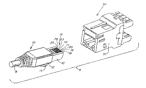
Fig. 1 shows a modular connector system 5, which
includes an RJ-type plug 10 and an RJ-type jack 30. Plug 10
includes an isolating shell 12 partially surrounding a
dielectric body 13 and a snap detent mechanism 14. Plug 10
includes eight plug contacts located in separate slots formed
in dielectric body 13 at a distal region 16. Plug contacts 18,
19, 20, 21, 22, 23, 24 and 25 may be directly connected to
eight plug connection terminals, or may be connected to a
compensation structure that is in turn connected to the plug
connection terminals. In either case, plug contacts 18, 19,
20, 21, 22, 23, 24 and 25 are electrically connected to eight
insulated conductors arranged in four twisted pairs and located
in a data transmission cable 8. Each plug connection terminal
may include an insulation displacement contact, which has sharp
points for cutting through the insulation to contact the metal
wire of one conductor, as is known in the art.
Jack 30 includes a jack housing 31 surrounding eight
signal carrying elements connected to eight cantilever spring
contacts 46, 48, 50, 52, 54, 56, 58 and 60 discussed in
connection with Figs. 3 through 4D. The cantilever spring
contacts may be connected directly to connection terminals, or
may be connected to different compensation structures described
below. When plug 10 is inserted into jack 30, the plug
contacts 25, 24, 23, 22, 21, 20, 19 and 18 individually contact
the corresponding cantilever spring contacts 46, 48, 50, 52,
54, 56, 58 and 60 and thus provide electrical connection.
11
CA 02291373 2001-10-02
,.
'd-X371-236
As mentioned above, the parallel, side-by-side
contacts, connecting plug 10 to and jack 30, cause cross-talk
by their capacitive and inductive coupling. To reduce this
cross-talk, both plug 10 and jack 30 may include various
compensation structures, designed to counter-couple and thus
electrically balance the frequency-dependent capacitive and
inductive coupling, which are frequency dependent. One
compensation structure may itself cause additional capacitive
or inductive coupling that is then balanced by another
compensation structure. The overall design of connector system
5 minimizes cross-talk and thus reduces data transmission
errors caused by parasitic effects at high frequencies.
Referring to Figs. 1A and 3, in one embodiment, jack
30 includes eight spring contacts, a jack housing 31, a
compensation insert 33 and a management bar 38 (optional).
Jack housing 31 is made of a front jack housing 31A, a rear
jack housing 31B (shown in Fig. 2) and one or several
dielectric parts including an optional heat-shrink tube all
schematically shown as a cover 31. Front jack housing 31A
includes plug-receiving cavity 32, which provides space for
cantilever spring contacts 46, 48, 50, 52, 54, 56, 58 and 60
(shown in Fig. 3). Compensation insert 33 includes a
dielectric body 34 surrounding eight signal-carrying and
compensation elements, such as compensation elements of lead
frame 35. In the embodiment of Fig. 1A, cantilever spring
contacts 46, 48, 50, 52, 54, 56, 58 and 60 extend from the
distal part of lead frame elements 35 shown without dielectric
body 34. Connection terminals 45, 47, 49, 51, 53, 55, 57 and
59 are located at the proximal part of lead elements 35.
Fig. 1A also shows management bar 38, which may be
used with plug 10, jack 30 or both. Various aspects of
management bar 38 and its use are described in Appendix A,
entitled "A Method and Apparatus for Adjusting the Coupling
12
i
'~ 64371-236 (S)
CA 02291373 2001-10-02
Reactances between Twisted Pairs for Achieving a Desired
Level of Crosstalk", and Appendix B, entitled "Fixture for
Controlling the Trajectory of Wires to Reduce Crosstalk",
both of which are attached to this application. Management
bar 38 includes eight guide channels 39a, 39b, 39c, 39d, 39e,
39f, 39g and 39h. The eight guide channels have
predetermined relative orientations arranged to guide the
individual untwisted conductors of cable 8. Connection
terminals 45, 57, 49, 51, 53, 55, 57 and 59 are made of U-
shaped elements arranged in two rows. The U-shaped
connection elements include inner blade surfaces that cut
through the insulation of each insulated conductor as
mentioned above. Similarly, plug 10 may include a
compensation structure, such as lead frame 35, with a
management bar. Additional information about plug 10 is
provided in Appendix A and Appendix C, entitled Impedance
Compensation for Cable and Connector, both of which are
attached to this application.
Fig. 2 shows the preferred embodiment of jack 30,
which includes two types of compensation structures.
Cantilever spring contacts 46, 48, 50, 52, 54, 56, 58 and
60 are soldered to a printed wiring board 37 (printed
circuit board), which in turn is electrically connected to
a printed wiring board 38. Printed wiring boards 37 and 38
include eight signal-carrying elements that are connected
to terminals 45b, 47b, 49b, 51b, 53b, 55b, 57b and 59b. The
eight signal-carrying elements are arranged to provide
capacitive or inductive compensation. Furthermore, jack 30
includes a compensation structure with a dielectric insert
65 and a capacitive compensation structure 90, which
provides additional capacitive compensation. Specifically,
cantilever spring contacts 46, 48, 50, 52, 54,
13
CA 02291373 2001-10-02
... "
~.-X4371-236
56, 58 and 60 are connected to capacitive plates 92, 94, 96,
98, 100 and 102 (shown in detail in Fig. 3), which are
separated by dielectric plates 66, 68, 70, 72 and 74.
Dielectric insert 65 is made of GE Valox 365, and dielectric
plates 66, 68, 72, 74 are about 0.04" thick.
Figs. 2A through 2H show in detail cantilever spring
contacts 46, 48, 50, 52, 54, 56, 58 and 60 together with
capacitive plates 92, 94, 96, 98, 100 and 102, all made of
phosphor bronze. Referring to Fig. 2A, cantilever contact 46
and plate 92 have the thickness of 0.12" and have the following
dimensions: a=0.012", b=0.155", r1=0.012", r2=0.015", c=0.11",
d=0.463", e1=0.025", fl=0.072", g1=0.132", hl=0.048", i1=0.039",
j 1=0 . 16" , a=22°, y=24° and k1=0 . 208"
Fig. 2B shows cantilever contact 48, which includes
no capacitive plate. Cantilever spring contact 48 has the
thickness of 0.12" as have all other spring contacts and
capacitive plates described below. Cantilever spring contact
48 has the following dimensions: a=0.012", b'=0.095",
r1=0.012", r2=0.015", c=0.11", a=22° and d2=0.417". Referring to
Fig. 2C, cantilever spring contact 50 is connected to plate 94,
both of which have the following dimensions: a=0.012",
b'=0.155", r1=0.012", r2=0.015", c=0.11", a=22°, Y=24°,
d3=0.483", e3=0.036", f3=0.038", g3=0.160", i3=0.05" j3=0.16",
and k3=0.219".
Referring to Fig. 2D, cantilever spring contact 52 is
connected to capacitive plate 98, both of which have the
following dimensions: a=0.012", b'=0.095", r1=0.012",
r2=0.015", c=0.11", d4=0.503", e4=0.036", f4=0.039", f'4=0.017",
g4=0.132", i4=0.039", j4=0.155", h4=0.051", h'4=0.026", a=22°,
y=24°, and k4=0.206"
14
CA 02291373 2001-10-02
64371-236(S)
Referring to Fig. 2E, cantilever spring contact 54
is connected to a plate 96, both of which have the following
dimensions: a=0.012", b=0.155", r1=0.012", r2=0.015", c=0.11"
a=22°, y=24°, d5=0.487" " ~~
e5=0.045 , f5=0.035 , g5=0.144 ,
is=0.088", j5=0.16", and k5=0.207". Referring to Fig. 2F,
cantilever spring contact 56 is connected to plate 100, both
of which have the following dimensions: a=0.012", b'=0.095",
r1=0 . 012" , r2=0 . 015" , c=0 . 11" , a=22°, y=24°, d6=0 .
483" ,
e6=0.036", f6=0.038", g6=0.16", i6=0.05", j6=0.16", and
k6=0 . 219" .
Fig. 2G shows cantilever spring contact 58, which
has the following dimensions: a=0.012", b=0.155", r1=0.012",
r2=0.015", c=0.11", a=22° and d7=0.417". Referring to Fig. 2H,
cantilever spring contact 60 is connected to plate 102, both
of which have the following dimensions: a=0.012", b'=0.095",
r1=0 . 012" , r2=0 . 015" , c=0 . 11" , a=22°, y=24°, da=0 .
463" ,
e8=0.025", f8=0.072", g8=0.132", he=0.048", ie=0.039",je=0.16",
and ka=0.28". The above dimensions are a starting point for
obtaining desired capacitances and inductances. These
dimensions may require adjustments to obtain the required
performance. Fig. 2I is a perspective view of the spring
contacts 46, 48, 50, 52, 54, 56, 58 and 60 individually shown
in Figs. 2A through 2H and the compensation structure with
capacitive plates 92, 94, 96, 98, 100 and 102.
In the embodiment of Fig. 3, jack 30 includes the
signal carrying and compensation elements (such as lead frame
35) hidden inside dielectric body 34 of compensation insert
33. Lead frame 35 is described in the PCT publication WO
94/21007. Connection terminals 45a, 47a,
CA 02291373 2001-10-02
64371-236 (S)
49a, 51a, 53a, 55a, 57a and 59a are located at the proximal
ends of signal carrying and compensation elements, and may be
soldered to a printed circuit board.
All signal-carrying and compensation structures used
in plug 10 or jack 30 include at least some of their signal-
carrying elements spaced and distributed in a three-dimensional
manner so that different elements are spaced not only laterally
along the length of the connector element, but also vertically
relative to the plane of the lateral spacing of the elements.
This arrangement is specifically designed to introduce a known
amount of capacitance and inductance into the individual
conductors. The compensation structures are arranged to
counter-couple and electrically balance out the capacitance and
inductance of each individual element and also balance out
mutual inductances and capacitances between the elements of
connector system 5. In this way, the compensation structures
reduce the overall cross-talk between the leads of connector
system 5, and thus they optimize its data transmission
performance.
Each compensation structure has a specific function
in cross-talk reduction. Data transmission cable 8 includes,
for example, four twisted pairs of insulated conductors. In
the body of cable 8, each conductor of a twisted pair is
affected substantially equally by adjacent conductors because
the pairs are twisted. However, when cable 8 terminates at
plug 10 or jack 30, the twisted pairs are untwisted and
flattened out so that several conductors form a substantially
linear arrangement. Here, a variable amount of deformation of
the individual conductors is required to align the conductors;
this deformation can be controlled by a management bar.
16
CA 02291373 2001-10-02
-04371-236
Notably, where a conductor is adjacent to another
conductor of an unrelated pair, electromagnetic coupling occurs
between adjacent conductors from different pairs. This
coupling introduces an interfering signal into one conductor of
a pair, but not an equal interfering signal into the other
conductors. This creates differential noise that is random
because of the random nature of the connector deformation that
depends on a place where cable 8 is terminated. The capacitive
imbalance due to the de-twisting region varies from 0 to 600
femtofarad. Optional management bar 38 and the management bar
used in plug 10 introduce a known and reproducible deformation
to the conductors. This known deformation and the structural
construction of the plug introduce a known amount of
capacitance and inductance between the conductors. The jack
compensation structures then compensate for this capacitance
and inductance and also compensate for the electric and
magnetic fields generated within the plug.
Referring to Figs. 3 through 4D, jack 30 includes a
compensation structure 90, which is arranged to provide
compensation signals to balance capacitances created in the
other compensation structures, or created in cantilever spring
contacts 46 through 60 and plug contacts 18 through 24.
Compensation structure 90 includes capacitive plates 92, 94,
96, 98, 100 and 102 substantially aligned with respect to each
other and separated by a dielectric. As shown in the
embodiments of Figs. 3A and 3D, capacitive plate 92 is
connected to spring contact 46, capacitive plate 94 is
connected to spring contact 50, capacitive plate 96 is
electrically connected to spring contact 54, capacitive plate
98 is electrically connected to spring contact 52, capacitive
plate 100 is electrically connected to spring contact 56, and
capacitive plate 102 is electrically connected to spring
contact 60. A crossover structure 95 (Figs. 3D and 4) provides
17
CA 02291373 2001-10-02
4371-236
a connection between capacitive plate 96 and spring contact 54,
and a crossover structure 97 provides a connection between
capacitive plate 98 and spring contact 52. In general, the
crossover structures can be placed at different locations of a
compensation insert 40 along the cantilever spring contacts.
Compensation structure 90 is located near contact
points between spring contacts 46 through 60 and the
corresponding and blade-shaped contacts 62 through 76. In this
arrangement, parallel capacitive plates 92 through 102 are
placed on the rear side of cantilever spring contacts 46
through 60 and outside the path taken by the current that
conveys the high frequency signal from the contact point of
plug 10 to jack 30 to the compensating structures in 34 of the
high frequency signal paths from plug 10 to jack 30.
Furthermore, the mutual inductance between the compensation
route and the signal-carrying route should remain small. The
compensation route is both short and significantly independent
of the flow direction of the high-frequency signal. The
relative area of capacitive plates 92 through 102, their
separation, and the dielectric located between the plates are
designed to achieve a desired counter-coupling level.
Referring to Figs. 3 and 3B, jack housing 31A
includes a comb structure 80, which maintains a uniform
separation between spring contacts 46 through 60. Jack housing
31 may also include a dielectric structure 65 (shown in Fig.
2), which provides a mechanical guide between capacitive plates
92 through 102 when plug 10 is inserted. The vertical
orientation of capacitive plates 92 through 102 makes them
relatively insensitive to movements of plug 10 within jack
receiving cavity 32. The vertical orientation also makes
capacitive plates 92 through 102 relatively insensitive to the
relative height of the mated connection imposed by the height
18
CA 02291373 2001-10-02
-X4371-236
of the contact areas of plug contacts 18, 19, 20, 21, 22, 23,
24 and 25.
As described above, connector system 5 provides a
connection for a high-frequency data transmission cable with
four twisted pairs of insulated conductors bundled into a round
profile, a flat profile or any other profile. The four twisted
pairs are connected to jack 30 in a convenient order and
orientation. For example, the insulated conductors of the A
pair are connected to contacts 51a and 53a, the conductors of
the B pair are connected to contacts 49a and 55a, the
conductors of the C pair are connected to contacts 45a and 47a,
and the conductors of the D pair are connected to contacts 57a
and 59a. That is, the A pair is connected to the middle two
cantilever spring contacts, the B pair straddles the A pair,
the C pair is on one side of the B pair, and the D pair is
positioned on the opposite side of the B pair. (The four
twisted pairs are also similarly connected to the corresponding
jacks contacts 18, 19, 20, 21, 22, 23, 24 and 25 shown in
Fig. 1). In this configuration, the B pair will encounter
cross-talk from the other three pairs because the B pair spring
contacts 40 and 46 are the only contacts that are in close
proximity to contacts of all of the other pairs of contacts.
As mentioned above, the conductors of each twisted
pair are driven differentially, wherein the two conductors
transmit signals with opposite polarity. When noise from
external sources couples to both wires nearly equally it forms
a common mode signal that propagates over the twisted pair. At
the receiving end, a differential amplifier amplifies the
differential signals carrying the data and attenuates the
common-mode signals. The amount of attenuation of the common-
mode signals by the differential amplifier is expressed as the
common-mode rejection ratio. The differential amplifier cannot
attenuate the differential cross-talk coupled into just one
19
CA 02291373 2001-10-02
44371-236
pair of conductors. The uniquely designed structures provide
counter-coupling that generates a compensation signal within a
twisted pair that balances, within the same twisted pair, an
interfering cross-talk signal arising from the neighboring
pair.
Referring to Fig. 3D, capacitive compensation
structure 90 makes the cross-talk signal more symmetric using
capacitive plates 92 through 102. In general, the compensation
structure couples spring connector 50 to spring connectors 46
and 54. Spring connectors 46 and 54 correspond to the second
wire in their respective wire pairs labelled C and A, where the
first wires in the pairs are connected to spring connectors 48
and 52. Similarly, the compensation structure couples spring
connector 56 to spring connectors 52 and 60. Spring connectors
52 and 60 correspond to the second wire in their respective
wire pairs labelled A and D, where the first wires in the wire
pairs are connected to spring connectors 54 and 58,
respectively.
Figs. 4 through 5A show different embodiments of the
capacitive compensating structures. Referring to Figs. 4 and
4A, compensation insert 33A includes a compensation structure
90A including six horizontal compensation plates. Like
compensation structure 90, compensation structure 90A is
arranged to provide compensation signals that balance cross-
talk generated in cantilever spring contacts 46 through 60 or
generated in jack contacts 66 through 80. Compensation
structure 90A includes capacitive plates 92A, 94A, 96A, 98A,
100A and 102A substantially aligned with respect to each other
and separated by a dielectric. Capacitive plate 92A is
connected to spring contact 46, capacitive plate 94A is
connected to spring contact 50, capacitive plate 96A is
electrically connected to spring contact 54, capacitive plate
98A is electrically connected to spring contact 52, capacitive
CA 02291373 2001-10-02
-.
04371-236
plate 100A is electrically connected to spring contact 56, and
capacitive plate 102A is electrically connected to spring
contact 60. A crossover structure 95 provides a connection
between capacitive plate 96 and spring contact 54, and a
crossover structure 97 provides a connection between capacitive
plate 98 and spring contact 52. Capacitive plate 94A, located
between plates 92A and 96A,provides capacitive coupling to
spring contacts 46 and 54. Capacitive plate 100A, located
between plates 98A and 102A, provides capacitive coupling to
spring contacts 52 and 60.
Fig. 4B is a side view of compensation insert 33A.
Compensation structure 90A may have several designs that vary
the capacitive counter-coupling. Compensation structure 90A
may have capacitive plates 92A, 94A, 96A, 98A, 100A, and 102A
aligned at a selected angle a with respect to the orientation
of the respective spring contacts 46, 48, 50, 52, 54, 56, 58
and 60, or aligned at a selected angle with respect to each
other (i.e., the capacitive plates need not be arranged in
parallel). The relative orientations of the plates are
selected to vary the amount of compensation (i.e., counter-
coupling effects) provided by the capacitive plates.
Fig. 4C is a perspective rear view of compensation
insert 33A with a compensation structure 91A. In compensation
structure 91A, capacitive plate 96A is located between plates
92A and 94A using a crossover structure 95A. Thus, capacitive
plate 96A provides capacitive coupling between spring contact
54 and spring contacts 46 and 50. Similarly, capacitive plate
102A is located between plates 98A and 100A using a crossover
structure lOlA. In this arrangement, capacitive plate 102A
provides capacitive coupling between spring contact 52 and
spring contacts 56 and 60. Fig. 4D is a top view of
21
CA 02291373 2001-10-02
.4371-236
compensation insert 33A using compensation structure 91A, shown
in Fig. 4C.
Figs. 5 and 5A are a perspective front view and a top
view, respectively, of a compensation insert 33B with a
compensation structure 90B. Compensation structure 90B
includes a capacitive plate 92B connected to spring contact 46,
a capacitive plate 94B connected to spring contact 50, and a
capacitive plate 96B connected to spring contact 54 using a
crossover structure 95B. Furthermore, compensation structure
90B includes a capacitive plate 98B connected to spring contact
60, capacitive plate 100B connected to spring contact 56, and
capacitive plate 102B connected to spring contact 52 using a
crossover structure 101B.
After plug 10 and jack 30 are mated, the position of
one plate relative to the adjacent plate can be adjusted by
varying the overlap between the plates. Compensation
structures 90, 90B are 91 are designed with a preselected
overlap or an adjustable overlap, for example, to be modified
for different types of plugs. The overlap varies the
capacitance between the plates and hence the amount of cross-
talk energy coupled between the contacts. Therefore, the
adjustment should be sufficient to balance cross-talk energy
among the connector terminals and establish cross-talk at the
desired level for the particular connector.
In general, plug 10 and jack 30 include compensation
structure that provide capacitive and inductive rebalancing.
The inductive rebalancing technique is described, for example,
in U.S. Pat. 5,326,284. Referring again to Fig. 1, plug 10
includes blade-like contacts 18, 19, 20, 21, 22, 23, 24 and 25,
which introduce mainly stray capacitance. There are
significant capacitive imbalances between the individual
contacts. For example, the capacitance between contacts 19 and
22
CA 02291373 2001-10-02
.1
X4371-236
20 is significantly higher than the capacitance between
contacts 18 and 20. When contacts 18 and 19 receive a purely
differential signal, described above, there are capacitively
induced electromotive forces in contact 20 causing currents
flowing in and out of contact 20 in direct relationship to the
signal applied to contacts 18 and 19. Contact 20 emits a
common mode signal of approximately one half of the signal
induced from contacts 18 and 19 into contact 20. Contact 20
also emits a differential signal of approximately one half of
the signal induced from contacts 18 and 19 into contact 20.
These two signals are further split into two signals, one
signal travelling backward and the other forward. Contact 24
also has a signal introduced from 18 and 19. However, since
contact 24 is farther than contact 20, the amplitude of the
involved signal on contact 24 is smaller. For example, this
capacitive imbalance can be compensated by coupling the same
signal from contacts 18 and 19 into contact 24 as is coupled
from contacts 18 and 19 into contact 20 of jack 10 (Fig. 1).
The capacitance between adjacent plates 19 and 20 is
on the order of C=460 femtofarad (fF). This capacitance is
partially neutralized by the smaller capacitance between plates
18 and 20. The residual capacitive imbalance is in the range
of 300 femtofarad (fF). It has the following corresponding
impedance X~= (j~C) -1, which is about X~=-j 500052 at frequencies
of 100 MHz. This is sufficient to cause serious cross-talk
problems. On the other hand, the blade-like contacts have a
very low, distributed inductance (XL) due to their flat and wide
surfaces. The characteristic impedance of the blade-like
contact structure is defined by XL/X~. Without compensation
structures 16 and 26, the blade-like contacts are directly
connected to twisted pairs of conductors that form transmission
lines of 10052. Thus, the characteristic impedance of the
blade-like structure is significantly lower than the
23
CA 02291373 2001-10-02
y
X4371-236
characteristic impedance of the terminated twisted pair cable.
For each wire there is the corresponding cross-talk isolation
P=20 log (50/5000) dB (~40 Db with a desired goal of 60 dB
crosstalk isolation).
Furthermore, there is a capacitive imbalance due to
the de-twisting region where the conductors transition from the
twisted pairs to the parallel conductor geometry connected to
the end terminals of plug 10. Here, the capacitance between
the wire conductors is on the order of 312 fF. The above-
described management bar makes this capacitance reproducible.
The signal generated by this capacitive imbalance adds to the
previous signals induced by the blade-like structure and
further reduces the crosstalk isolation down to about -38 dB at
100 MHz. Therefore, compensation structures 90, 90A, 90B or 91
are designed to provide counter-coupling for capacitive
imbalances created in plug 10.
24