Note : Les descriptions sont présentées dans la langue officielle dans laquelle elles ont été soumises.
CA 02291692 1999-11-29
k
SPECIFICATION
COMMUNICATION EQUIPMENT
Technical Field
The present invention relates to a communication
system for controlling terminal units through boundary
scan elements, and particularly to a communication system
which can quickly transmit output data from the terminal
units.
Back~;round of the Invention
A boundary scan test method has been proposed as one
of the inspection methods with a plurality of IC chips
arranged over a printed wire board with printed wiring
formed thereon, to see whether or not connection between
each IC chip and each printed wiring is properly made and
whether or not each printed wiring is not broken.
This boundary scan test method can be applied to
integrated circuits (IC chips) into which boundary scan
elements are incorporated. The boundary scan element, for
example as shown in Fig. 4, includes a plurality of
boundary cells 114 individually provided between
input/output terminals of an internal logic 111 for
implementing the inherent functions of the integrated
circuit 110 and input/output terminals 112/113 of the
integrated circuit 110, a TAP controller (TAP circuit) 119
for controlling input and output of data to or from the
boundary cells 114, a TDI terminal 120 for receiving test
data, a TDO terminal 121 for transmitting test data, a TCK
terminal 122 into which a clock signal is input, and a TMS
1
CA 02291692 1999-11-29
terminal 123 for receiving a mode signal for switching the
operation mode of the TAP controller 119; and, if required,
it is further provided with a bypass register 115, an ID
CODE register 116, an instruction register 117, a TRS
terminal 124 for receiving a reset signal, or the like.
In this connection, the bypass register 115 to instruction
register 117 is referred to as boundary scan register
( 118 ) .
To describe the respective terminals or the signals
to be input/output through the respective terminals in
detail, TDI (Test Data In) is a signal for serial-
inputting instructions and data to a test logic, and is
sampled at rising edges of TCK. TDO (Test Data Out) is a
signal for serial-outputting data from the test logic, the
output value being changed at falling edges of TCK. TCK
(Test Clock) supplies a clock to the test logic. It is a
dedicated input for enabling the use of a serial test data
path independent of the system clock inherent to the
component. TMS (Test Mode Select) is a signal for
controlling the test operation, and is sampled at rising
edges of TCK. The TAP controller decodes this signal.
TRST (Test Reset) is a negative logic symbol for
asynchronously initializing the TAP controller, and is
optional.
The integrated circuit 110 into which such boundary
scan element is incorporated can be tested on the
operating state thereof and the connecting relationship
between this integrated circuit 110 and external devices,
by the procedures described below.
2
CA 02291692 1999-11-29
4
First, in checking the quality of the internal logic
111 of the integrated circuit 110, serial data (test data)
are input to the TDI terminal 120 of the integrated
circuit 110 as they are shifted, and thereby the test data
are set into the respective boundary cells 114
corresponding to the respective input terminals 112. In
this state, the integrated circuit 110 is operated before
the data set in the respective boundary cells 114
corresponding to the respective output terminals 113 are
shifted for output from the TDO terminal 121, and, on the
basis of the corresponding relationship between the serial
data (test result data) thus obtained and the test data
input to this integrated circuit 110, the internal logic
111 of the integrated circuit 110 is tested for its
quality.
The boundary scan test method can also be carried
out on a plurality of integrated circuits as long as the
boundary scan elements are incorporated therein.
For example, a plurality of integrated circuits 110
mounted on a substrate 126 as shown in Fig. 5 can also be
subjected to a test for breakage and the like of the
printed patterns between the integrated circuits 110,
along with a test on the integrated circuits 110
themselves.
In this case, the respective boundary scan elements
incorporated in the plurality of integrated circuits 110
are connected in series with each other. Specifically,
the TDO terminal 121 of the first integrated circuit 110
(the left in the drawing) and the TDI terminal 120 of the
3
CA 02291692 1999-11-29
a '
second integrated circuit 110 (the right in the drawing)
are connected with each other, the output terminal 129 of
a boundary scan controller board 128 provided in host
computer unit 127 or the like and the TDI terminal 120 of
the first integrated circuit 110 are connected with each
other, and the input terminal 130 of the boundary scan
controller board 128 and the TDO terminal 121 of the
second integrated circuit 110 are connected with each
other. The test procedures are as follows:
In testing breakage, short circuit, and the like of
the printed patterns, a test data preparing tool 131 or
the like is used to prepare test data (serial data), which
is output from the output terminal 129 of the boundary
scan controller board 128 and is input to the TDI terminal
120 of the first integrated circuit 110 while shifted,
setting the test data into the respective boundary cells
114 corresponding to the respective output terminals 113
in this integrated circuit 110. In this state, the data
stored in these respective boundary cells 114 are output
from the respective output terminals 113 provided in the
first integrated circuit 110 as shown in Fig. 6, and are
input through the respective printed patterns 133
constituting a system bus and the like to the respective
input terminals 112 of the second integrated circuit 110,
and further fetched into the respective boundary cells 114
corresponding to these respective input terminals 112.
Thereafter, the data stored in the respective
boundary cells 114 of these respective integrated circuits
110 are shifted and fetched through the input terminal 130
4
CA 02291692 1999-11-29
of the boundary scan controller board 128 as they are
analyzed by using a test result analyzing tool 132 or the
like, so that a test can be made for breakage, short
circuit, and the like in such a test range 135 as the
printed patterns 133 providing connection between the
integrated circuits 110.
Next, in inspecting the internal logic 111 of the
respective integrated circuits 110, test data are output
from the output terminal 129 of the boundary scan
controller board 128, and are input to the TDI terminal
120 of the first integrated circuit 110 as they are
shifted, so as to be set into the respective boundary
cells 114 corresponding to the respective input terminals
112 of this integrated circuit 110 as shown in Fig. 8.
Subsequently, this integrated circuit 110 is
operated, and the resulting data are fetched into the
respective boundary cells 114 corresponding to the
respective output terminals 113 before the data stored in
these respective boundary cells 114 are shifted to be
output from the TDO terminal 121 of the first integrated
circuit 110. Here, the second integrated circuit 110 is
brought into a bypass state as shown in Fig. 7 by the
boundary scan controller board 128, so that the data
output from the TDO terminal 121 are bypassed through the
second integrated circuit 110 and fetched through the
input terminal 130 of the boundary scan controller board
128. Then, the test analyzing tool 132 or the like can be
used for analysis of the fetched data to test whether or
not the first integrated circuit 110 operates properly.
5
CA 02291692 1999-11-29
Next, in the cases of inspecting the second
integrated circuit 110, the boundary scan controller board
128 similarly brings the first integrated circuit 110 into
a bypass state as shown in Fig. 7 before test data are
output from the output terminal 129 of the boundary scan
controller board 128 and bypassed through the first
integrated circuit 110. Then, the test data are input to
the TDI terminal 120 of the second integrated circuit 110
while shifted, to be set into the respective boundary
cells 114 corresponding to the respective input terminals
112 of this integrated circuit 110 as shown in Fig. 8.
Subsequently, this integrated circuit 110 is operated, and
the resulting data are fetched into the respective
boundary cells 114 corresponding to the respective output
terminals 113. Thereafter, the data stored in the
respective boundary cells 114 are shifted to be output
from the TDO terminal 121, and further fetched through the
input terminal 130 of the boundary scan controller board
128. Then, the fetched data can be analyzed by using the
test result analyzing tool 132 and the like, so as to test
whether or not the second integrated circuit 110 operates
properly.
In this way, a substrate 126, as long as using
integrated circuits 110 into which boundary scanning
circuits are incorporated, can be tested for the quality
of the respective integrated circuits 110 themselves and
on the connecting relationship between the integrated
circuits 110 and the like by conducting the boundary scan
test method.
6
CA 02291692 1999-11-29
Now, it was found by the present inventor that when
integrated circuits into which such boundary scan elements
are incorporated are used to constitute the substrate or
the like of a sensor module, input and output of serial
data can be made to or from the respective integrated
circuits mounted on the substrate 126 at a rate on the
order of 20 Mbps without the use of communication
integrated circuits or the like.
Then, a communication system was proposed which
applies the boundary scan elements to carry out
communication with host computer units and the like
without the use of communication devices.
Fig. 9 is a block diagram showing an example of the
communication system to which the boundary scan elements
are applied.
The communication system 140 shown in this figure
includes: a communication controller device 141 for
carrying out the transmitting of control data, the
collection of detected data, and the like; a plurality of
sensor units 142a-142c for carrying out the monitoring of
an object to be monitored; a plurality of boundary scan
elements 143a-143c provided for each of these sensor units
142a-142c, the boundary scan elements carrying out such
processing as fetching the control data output from the
aforesaid communication controller device 141 to supply
the same to the respective sensor units 142a-142c, and
fetching the detected data or the like output from these
respective sensor units 142a-142c to supply the same to
the aforesaid communication controller device 141; and
7
CA 02291692 1999-11-29
communication lines 144 for providing connection between
each of these boundary scan elements 143a-143c and the
aforesaid communication controller device 141. The
boundary scan elements are connected in series to the
communication controller device 141. Specifically, the
connection is made in such a manner that the output
terminal 141a of the communication controller device 141
is connected to the TDI terminal of the boundary scan
element 143a, the TDO terminal of the boundary scan
element 143a connected to the TDI terminal of the next
boundary scan element 143b, and so on, and the TDO
terminal of the boundary scan element 143c is connected to
the input terminal 141b of the communication controller
device 141.
The function of this communication system 140 is as
follows:
The respective boundary scan elements 143a-143c
function in synchronization with the clock signal
transmitted from the TCK terminal 141d of the
communication controller device 141, and the operation
mode of each TAP controller is switched by the TMS signal
transmitted from the TMS terminal 141c of the
communication controller device 141.
Now, in driving the respective sensor units 142a-
142c according to the instruction from the host computer
unit 145, control data (serial data) are output from the
output terminal 141a of the communication controller
device 141, and they are supplied to the respective
boundary scan elements 143a-143c and set into the boundary
8
CA 02291692 1999-11-29
cells corresponding to the output terminals. Then, the
control data set are output from the output terminals, and
supplied to the respective sensor units 142a-142c
corresponding to the respective boundary scan elements
143a-143c, thereby driving these units.
Moreover, in the cases of collecting the detected
data from the respective sensor units 142a-142c according
to the instruction from the host computer unit 145, the
detected data of the respective sensor units 142a-142c are
once set in the respective boundary cells corresponding to
the input terminals of the corresponding, respective
boundary scan elements 143a-143c. Then, they are output
as serial data from the TDO terminals, and fetched through
the input terminal 141b of the communication controller
device 141.
Such communication system 140, when setting control
data into the respective boundary scan elements 143a-143c
or when outputting the detected data from the respective
boundary scan elements 143a-143c, can be maximized to 20
Mbps in data transfer rate, thereby allowing the transfer
of communication data at higher rates than those of
conventional communication systems.
However, the communication system described above
had a problem in that when the detected data of the
terminal units such as sensor units connected to the
boundary scan elements are enormous, e.g. picture signals
and the like, a drop in the transfer rate is undeniable
and the effect of the high-rate data transfer obtained by
the application of the boundary scan elements as
9
CA 02291692 1999-11-29
communication elements is not exerted sufficiently.
Moreover, since the boundary scan elements can only
input and output information in the form of digital
signals, there was a problem in that they cannot fetch
information in an analog signal form.
~um_ma_r~r of 'h Inv .nti nn
An object of the present invention is to provide a
communication system which can transfer data from terminal
units at higher rates.
Another object of the present invention is to
provide a communication system which can transfer analog
signals from terminal units at higher rates.
According to the present invention, there is
provided a communication system comprising: a plurality of
boundary scan elements including a plurality of boundary
cells individually assigned to respective input terminals
and output terminals, a TAP circuit for controlling input
and output of data to or from the aforesaid boundary cells,
a TDI terminal for inputting serial data to be supplied to
the aforesaid boundary cells, a TDO terminal for
outputting data from the aforesaid boundary cells in the
form of serial data, a TCK terminal into which a clock
signal is input, and a TMS terminal into which a mode
signal for switching the operation mode of the aforesaid
TAP circuit is input; a plurality of terminal units each
connected with each of the aforesaid boundary scan
elements or provided with an IC into which each of the
elements are incorporated; and a communication controller
connected with the aforesaid boundary scan elements in
CA 02291692 1999-11-29
series for transmitting/receiving through the aforesaid
boundary scan elements control data for individually
controlling the aforesaid terminal units, characterized in
that the aforesaid terminal units are connected in
parallel and a single data communication line for
transmitting output data of the aforesaid terminal units
to the aforesaid communication controller is provided
(claim 1).
In the present invention, the communication
controller controls the terminal units by transmitting
control data thereto through the boundary scan elements.
Then, data obtained by the terminal units are directly
transmitted to the communication controller through the
data communication line without the intermediary of the
boundary scan elements.
This enables the high-rate transfer of data even
when the output data of the terminal units are enormous,
and allows the transfer of the output data even when they
are analog signals.
Moreover, the output data are transmitted through a
single data communication line, so that wiring of the
system is simplified. In addition, the boundary scan
elements are driven synchronously, so that when the
respective terminal units are switched to transmit their
output data through the data communication line, little
time rag is produced between the output data and
interference therebetween is avoided.
In the present invention, the terminal units include
various sensor units, such as monitoring camera units, and
11
CA 02291692 1999-11-29
the output data include the detected data of the sensor
units, such as moving picture signals and still picture
signals.
The control data include not only the data to be
transmitted to the terminal units for the control of the
terminal units, but also the status data and the like of
the terminal units to be transmitted back from the
terminal units.
The boundary scan elements include not only
independent, separate packages but also those incorporated
in other ICs. Besides, the input terminals and output
terminals represent, in the case where each of the
boundary scan elements is an independent package, the
input terminals and output terminals thereof, and
represent, in the case where the boundary scan elements
are incorporated into other ICs, the input terminals and
output terminals of the ICs. Then, the aforesaid output
terminals and the aforesaid input terminals are connected
to the input terminals and the output terminals of the
terminal units, respectively, so that the data of the
boundary cells are output to the terminal units and data
are conversely input to the boundary cells.
Moreover, according to the present invention, the
communication system described above may be provided in
which: the output data are analog signals; and an analog
signal processor for processing the output data may be
provided between the communication controller and the
communication line (claim 2). In this invention, the
provision of the aforesaid analog signal processor can
12
CA 02291692 1999-11-29
ease the load on the communication controller to quickly
perform the processing of analog signals.
Furthermore, according to the present invention,
there is provided the above-described communication system
in which: the boundary cells include a plurality of input-
terminal-side boundary cells connected in series and
assigned to the respective input terminals individually,
and a plurality of output-terminal-side boundary cells
connected in series and assigned to the respective output
terminals individually; and the input-terminal-side
boundary cells and the aforesaid output-terminal-side
boundary cells are connected in parallel between the TDI
terminal and the TDO terminal (Claims 3).
In this invention, the boundary cells are not
coupled all in series as conventionally, but are divided
into the input-terminal-side boundary cells assigned to
the input terminals and the output-terminal-side boundary
cells assigned to the output terminals, which are
connected in parallel between the TDI terminal and the TDO
terminal. Accordingly, for example, when data from the
TDI terminal are being set into the output-side boundary
cells, direct transfer of the data to the output-side
boundary cells can be made without the intermediary of the
aforesaid input-terminal-side boundary cells, which can
further realize the higher-rate transfer of data between
the boundary scan elements and the communication
controller or the terminal units.
$_ri_ef De' rintinn pf the Drawin~~
Fig. 1 is a block diagram showing a first embodiment
13
CA 02291692 1999-11-29
of the communication system of the present invention;
Fig. 2 is a block diagram showing a second
embodiment of the communication system of the present
invention;
Fig. 3 is a block diagram of the boundary scan
element lla-llc in Fig. 2;
Fig. 4 is a block diagram of a conventional boundary
scan element;
Fig. 5 is a block diagram showing an example of a
boundary scan test using the boundary scan elements shown
in Fig. 4;
Fig. 6 is a schematic diagram showing an example of
a boundary scan test using the boundary scan elements
shown in Fig. 4;
Fig. 7 is a schematic diagram showing an example of
a boundary scan test using the boundary scan elements
shown in Fig. 4;
Fig. 8 is a schematic diagram showing an example of
a boundary scan test using the boundary scan elements
shown in Fig. 4; and
Fig. 9 is a block diagram showing an example of a
conventional communication system to which boundary scan
elements are applied.
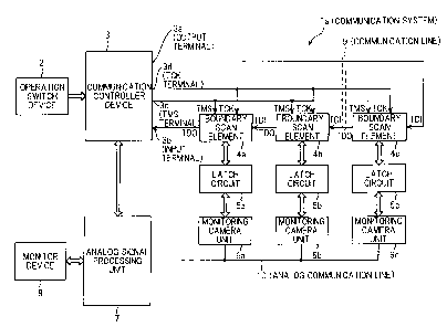
« Configuration of First Embodiment »
Fig. 1 is a block diagram showing a first embodiment
of the communication system of the present invention.
The communication system la shown in this figure
includes a plurality of boundary scan elements 4a-4c,
14
CA 02291692 1999-11-29
monitoring camera units (terminal units) 6a-6c connected
with the respective boundary scan elements 4a-4c through
latch circuits 5a-5c, a communication controller device 3
for controlling the monitoring camera units 6a-6c through
the boundary scan elements 4a-4c, a single analog
communication line (data communication line) 10 through
which picture signals of the monitoring camera units 6a-6c
are transmitted, and an analog signal processing unit 7
for receiving the picture signals transmitted from the
analog communication line 10; furthermore, to the
communication controller device 3 is connected an
operation switch device 2, and to the analog signal
processing unit 7 is connected a monitor device 8 for
displaying the picture signals output from the monitoring
camera units 6a-6c.
The boundary scan elements 4a-4c have the same
configuration as that shown in Fig. 4, and are connected
in series to the communication controller device 3.
Specifically, the output terminal 3a of the communication
controller device 3 is connected to the TDI terminal of
the boundary scan element 4c, the TDO terminal of the
boundary scan element 4c is connected to the TDI terminal
of the next boundary scan element 4b, and the TDO terminal
of the boundary scan element 4b is similarly connected to
the TDI terminal of the boundary scan element 4a. Finally,
the TDO terminal of the boundary scan element 4a is
connected to the input terminal 3b of the communication
controller device 3. Accordingly, the data being supplied
to the boundary scan elements 4a-4c or the data being
CA 02291692 1999-11-29
output from the boundary scan elements 4a-4c are always
transferred in the direction from the boundary scan
elements 4c to 4a.
Further, the TCK terminal and the TMS terminal of
each of the boundary scan elements 4a-4c are supplied with
a clock signal and a mode signal from the communication
controller device 3, respectively, and thereby the
respective boundary scan elements 4a-4c function
synchronously.
The input terminals and output terminals (not shown)
of the boundary scan elements 4a-4c are connected with the
corresponding latch circuits 5a-5c, respectively. Control
data set in the boundary cells are output through the
respective latch circuits 5a-5c to the corresponding
monitoring camera units 6a-6c, and the status data of the
monitoring camera units 6a-6c, such as data indicating
whether the monitoring operation is in action or not, data
indicating the direction of monitoring, and data
indicating the magnitude of the shooting lens, are input
through the latch circuits 5a-5c to the boundary cells.
The monitoring camera units 6a-6c are arranged at
positions corresponding to objects to be monitored, carry
out the shooting of the objects to be monitored while
switching the shooting directions and the magnitude of the
shooting lens in accordance with the control data output
from the corresponding latch circuits 5a-5c, and transmit
back to the corresponding latch circuits 5a-5c the
shooting conditions and the like as the status data. In
addition, the monitoring camera units 6a-6c directly
16
CA 02291692 1999-11-29
transmit the picture signals obtained by the shooting to
the analog communication line 10 without the intermediary
of the latch circuits 5a-5c.
The communication controller device 3 includes
hardware circuits, microprocessor circuits, and the like,
and transmits control data to the respective boundary scan
elements 4a-4c in accordance with selection indication
data output from the operation switch device 2, thereby
controlling the monitoring camera units 6a-6c. It also
receives the status data from each of the boundary scan
elements 4a-4c, and analyzes the same to check whether or
not the monitoring camera units 6a-6c are functioning
normally, and the like. Moreover, it controls the analog
signal processing unit 7 in accordance with the selection
indication data output from the operation switch device 2,
so that the picture signals transmitted from the analog
communication line 10 are displayed on the monitor device
8.
The analog communication line 10 is composed of a
coaxial cable and the like, and connects between the
analog signal input terminal of the analog signal
processing unit 7 and the analog signal output terminals
of the respective monitoring camera units 6a-6c in
parallel. And, it fetches a picture signal output from
any one of the monitoring camera units 6a-6c, and
transmits the same to the analog signal input terminal of
the analog signal processing unit 7.
The analog signal processing unit 7 includes an
analog signal input circuit for fetching a picture signal,
17
CA 02291692 1999-11-29
an analog signal processing circuit for applying
designated image processing to the picture signal fetched
by this analog signal input circuit, a picture signal
output circuit for outputting the picture signal image-
s processed by this analog signal processing circuit in the
form of an analog signal or in the form of a digital
signal, and a control circuit for controlling these
circuits in accordance with operation indication signals
from the communication controller device 3, and the like.
In accordance with instructions output from the
communication controller device 3, this analog signal
processing unit 7 fetches a picture signal supplied
through the analog communication line 10, and superimposes
thereon a status determination result and the like of the
respective monitoring camera units 6a-6c supplied from the
communication controller unit 3 before supplying the same
to the monitor device 8 in a designated signal form among
the analog signal form or the digital signal form.
The operation switch device 2 have a plurality of
push button switches and the like, generates selection
indication data and the like for selecting the monitoring
camera units 6a-6c and the like in accordance with the
operation content of the respective push button switches,
and supplies the same to the aforesaid communication
controller device 3. A user can operate this operation
switch device 2 to make the communication system la
execute particular processing.
The monitor device 8 is constituted by a CRT unit,
liquid crystal display unit, or the like having a display
18
CA 02291692 1999-11-29
capacity required to display pictures of the objects to be
monitored, and fetches the picture signal in the analog
signal form or picture signal in the digital signal form
output from the analog signal processing unit 7 to
displays the picture expressed by this picture signal.
K Operation of First Embodiment »
Next, referring to the block diagram shown in Fig. 1,
the operation of the communication system la will be
described in detail. The communication system 1a can be
manually switched to display the picture and the like of
any monitoring camera unit 6a-6c desired, and can be
automatically switched to display the picture and the like
of the respective monitoring camera units 6a-6c in
rotation.
<Manual Switching Operation of Monitoring Camera
Units 6a-6c>
When manual selection indication data are
transmitted from the operation switch device 2 to the
communication controller device 3, the communication
controller device 3 prepares control data required to turn
on one of the monitoring camera units 6a-6c designated by
the manual selection indication data and to turn off the
other monitoring camera units 6a-6c. These control data
are then transmitted through the communication lines 9 and
set into the boundary cells on the output Bides of the
respective boundary scan elements 4a-4c.
At the same time, from the communication control
device 3 to the analog signal processing unit 7 is output
an operation indication signal indicating a fetch
19
CA 02291692 1999-11-29
instruction for a picture signal, which makes the analog
signal processing unit 7 ready for the fetching operation
of picture signals.
Next, when a mode signal indicating an output
instruction for control data is output from the TMS
terminal 3c of the communication controller device 3, the
control data set in the boundary cells on the output sides
of the respective boundary scan elements 4a-4c are output
to the corresponding latch circuits 5a-5c, and further
transmitted to the respective monitoring camera units 6a-
6c. According to the content of the control data received,
each of the monitoring camera units 6a-6c recognizes
whether signal output permission is issued or not, and
only one of the monitoring camera units, e.g. the
monitoring camera unit 6c, transmits its picture signal
onto the analog communication line 10. The picture signal
transmitted is fetched into the analog signal processing
unit 7, and, further, a picture according to that picture
signal is displayed on the monitor device 8.
Subsequently, unless the operation switch device 2
is operated, the monitoring camera units 6a-6c hold their
states; and when the remaining monitoring camera unit 6a
or 6b is selected, manual selection indication data are
newly prepared, and the picture of either monitoring
camera unit 6a-6c selected is displayed on the monitor 8
through the procedures described above.
<Automatic Switching Operation of Monitoring Camera
Units 6a-6c>
When automatic selection indication data are
CA 02291692 1999-11-29
transmitted from the operation switch device 2 to the
communication controller device 3, the communication
controller device 3 prepares control data required to turn
on one of the monitoring camera units 6a-6c and to turn
off the other monitoring camera units 6a-6c. This is
followed by the same processing as that in the initiative
switching operation described above, so that the picture
of the monitoring camera unit selected, e.g. 6a, is
displayed on the monitor 8.
Then, after elapse of a certain time set in advance,
the communication controller device 3 prepares control
data required to turn on the monitoring camera unit 6b
which follows the monitoring camera unit 6a selected
initially and to turn off the remaining monitoring camera
units 6a and 6c. These control data are transmitted
through the communication lines 9, and the picture of the
monitoring camera unit 6b is displayed on the monitor 8
through the same processing as that in the case described
above.
Thereafter, the selecting operations for the
respective monitoring camera units 6a-6c described above
are cyclically repeated at each elapse of the certain time
set in advance, so that the pictures obtained by the
respective monitoring camera units 6a-6c are sequentially
displayed on the monitor device 8.
<Status Detecting Operation of Monitoring Camera
Units 6a-6c>
Here, in parallel to the manually-/automatically-
switched picture fetching operation or the image display
21
CA 02291692 1999-11-29
operation of the respective monitoring camera units 6a-6c
described above, status data indicating the operation
status and the like are output from the respective
monitoring camera units 6a-6c. These status data are
latched by the corresponding latch circuits 5a-5c before
transmitted to the input terminals of the respective
boundary scan elements 4a-4c and set into the boundary
cells.
Subsequently, when a TMS signal indicating a read
instruction is output from the TMS terminal 3c of the
communication controller device 3, the status data set in
the boundary cells are serially transferred from the TDO
terminals and supplied to the input terminal 3b of the
communication controller device 3.
The communication controller device 3 analyzes the
status data received, and makes judgements as to the
shooting conditions of the respective monitoring camera
units 6a-6c, whether or not the respective monitoring
camera units 6a-6c are functioning normally, whether or
not the communication lines 9 or the like are not broken,
or the like. These respective detection results and
respective judgement results can also be displayed on the
monitor device 8 through the analog signal processing unit
7.
« Effect of First Embodiment »
As has been described above, in the first embodiment
of the present invention, the picture signals transmitted
from the monitoring camera units 6a-6c are directly
transmitted to the analog signal processing unit 7 through
22
CA 02291692 1999-11-29
the analog communication line 10 without the intermediary
of the boundary scan elements 4a-4c. This allows the
high-rate transfer and processing of picture signals
without impairing the effect of the high-rate data
transfer due to the use of the boundary scan elements 4a-
4c. Moreover, the picture signals of the plurality of
monitoring camera units 6a-6c can be transmitted by a
single analog communication line 10, with the result of
simple wiring; besides, the synchronous functioning of the
boundary scan elements 4a-4c avoids the time rags and
interference to the picture signals in switching the
monitoring camera units 6a-6c.
<G Configuration of Second Embodiment »
Fig. 2 is a block diagram showing a second
embodiment of the communication system according to the
present invention.
The difference between the communication system lb
shown in this figure and the communication system 1a shown
in Fig. 1 consists in that specially-designed boundary
scan elements 11a-llc are used in place of the boundary
scan elements having the constitution shown in Fig. 4;
this realized the speed-up of the transfer of control data
and the like. Other configurations and functions are the
same as those of the communication system 1a; and to the
same parts are assigned the same numerals in Fig. 2.
Hereinafter, concrete description will be made on the
boundary scan elements 11a-11c.
As shown in Fig. 3, each of the boundary scan
elements lla-11c is incorporated into a chip case 12 as a
23
CA 02291692 1999-11-29
single package, and includes, similarly to the boundary
scan element shown in Fig. 4, boundary cells 19 and 20, a
TAP controller 25 for controlling input and output of data
to or from the boundary cells 19 and 20, a TDI terminal 14
for receiving serial data, a TDO terminal 15 for
transmitting serial data, a TCK terminal 17 into which a
clock signal is input, and a TMS terminal 16 for receiving
a mode signal for switching the operation mode of the TAP
controller 25; and, if required, it is further provided
with a bypass register 2l, an ID CODE register 22, an
instruction register 23, and the like (boundary scan
resister 24).
In the boundary scan elements lla-llc of Fig. 3,
however, the boundary cells 19 and 20 are not connected
all in series, and are divided into output cells (output-
side boundary cells) 20 and input cells (input-side
boundary cells) 19 corresponding to the output terminals
18 and input terminals 13 arranged on the exterior of the
chip case 12, respectively. The input cells 19 and the
output cells 20 are individually connected in series, and
are connected in parallel between the TDI terminal 14 and
the TDO terminal 15.
Then, as a special operation, the boundary scan
elements lla-11c have a mode in which either the input
cells 19 or the output cells 20 alone are brought into
their operative states and the other are brought into
their non-operative states.
Thereby, when the respective input cells 19 are put
in their operative states, the status data and the like
24
CA 02291692 1999-11-29
fetched into the respective input cells 19 through the
respective input terminals 13 can be directly output from
the TDO terminal 15 without being shifted through the
output cells 20 as conventionally.
~ Moreover, when the respective output cells 20 are in
their operative states, the control data and the like
input to the TDI terminal 14 can be shifted and set
directly into the respective output cells 20, and output
from the respective output terminals 18 to the external,
without being shifted through the input cells 19 as
conventionally.
By the use of the operation mode inherent in the
boundary scan elements 11a-11c described above, the
communication system lb composed of such boundary scan
elements 11a-llc is further improved in the data transfer
rate between the communication controller device 3 and the
respective boundary scan elements lla-11c as compared with
the communication system 1a described above.
« Other Embodiments»
Further, while in the first and second embodiments
described above, the picture signals in the analog signal
form are output from the respective monitoring camera
units 6a-6c and they are input through the analog
communication line 10 to the analog signal processing unit
7, picture signals in the digital signal form may be
output from the respective monitoring camera units 6a-6c
and they may be input through a digital communication line
(or a bus, an optical fiber cable, or the like) to a
digital signal processing unit.
CA 02291692 1999-11-29
In addition, while in the first and second
embodiments described above, the monitoring camera units
6a-6c are controlled as the terminal units of the
communication systems la and lb, other terminal units e.g.
a measuring device for measuring physical values of the
objects to be monitored, individual computer unit in
distributional arrangement, and the like may be controlled
to collect measurement, processing results, and the like
output from these respective measuring devices and
respective computer unit.
26