Note : Les descriptions sont présentées dans la langue officielle dans laquelle elles ont été soumises.
CA 02292542 1999-12-06
WO 98/58228 PCT/US98/12112
ELECTRONIC CIRCUITRY FOR TIMING AND DELAY CIRCUITS
BACKGROUND OF THE INVENTION
S Field of the Invention
The present invention pertains to electronic delay detonators and, in
particular,
to programmable electronic initiation delay detonators.
Electronic detonators are known for use in initiating explosive charges, e.g.,
for initiating booster charges used in mining and excavation applications.
Such deto-
nators are known for their precise delay characteristics relative to more
traditional
chemical-based delay units.
Related Art
U.S. Patent 5,377,592 to Rode et al, dated January 3, 1995, discloses an elec-
tronic digital delay unit powered by a pulse of energy generated by a
piezoelectric
transducer in response to an impulse-type initiation signal. The initiation
signal
stimulates the piezoelectric transducer to create a charge of electrical
energy that is
stored in a storage capacitor. Energy is drawn from the storage capacitor to
run a
timer circuit comprising an oscillator and a counter that counts oscillation
pulses from
the oscillator to a predetermined count. When the predetermined count is
reached, a
signal is generated to discharge the remaining energy from the storage
capacitor to the
electric igniter element, e.g., an exploding bridgewire. The detonator may be
equipped with an externally accessible programming interface so that the timer
circuit
may be programmed with a delay after the detonator is constructed.
U.S. Patent 5,435,248 to Rode et al, dated July 25, 1995, discloses an elec-
tronic range digital delay detonator comprising fusible links that are used to
perma-
nently program a desired function delay into the detonator circuit.
Electronic detonators of the type described in aforesaid U.S. Patent 5,435,248
and U.S. Patent 5,377,592 comprise conventional oscillators and counters.
CA 02292542 2003-02-04
2
SUMMA~?Y OF THE INVENTION
In one aspect, the present invention provides several novel features that find
utility in electronic delay detonators. One feature of the present invention
relates to an
oscillator circuit for generating a clock signal comprising a series of clock
pulses. The
oscillator circuit comprises a reference voltage means for producing a
reference
voltage. There are at least two capacitors in the oscillator, each capacitor
having one
of a charged state and a discharged state relative to the reference voltage. A
capacitor
in the discharged state has a voltage less than the reference voltage and is
designated a
discharged capacitor, and a capacitor in the charged state has a voltage that
exceeds
the reference voltage and is designated a charged capacitor. There is a
charging means
for charging a discharged capacitor to a charged state and a discharging means
for
discharging a charged capacitor, designated a charged working capacitor, to a
discharged state. The oscillator further comprises a comparator for generating
an
internal signal each time a charged working capacitor becomes a discharged
capacitor.
1 '> There is a switching means for performing a switching function comprising
effectively disconnecting a discharged capacitor from the discharging means
and
connecting it to the charging means, and for effectively disconnecting a
charged
capacitor from the charging means and connecting it to the discharging means,
and a
latch for issuing a clock pulse in response to the internal signals. The
switching means
may be responsive to the latch, for performing the switching function in
response to
clock pulses issued by the latch.
In accordance with another aspect of the present invention, there is provided
an oscillator circuit for generating a clock signal comprising a series of
clock pulses,
the circuit comprising:
(a) a reference voltage means for producing a reference voltage;
(b) at least two capacitors, each capacitor having one of a charged state
and a discharged state relative to the reference voltage, a capacitor in the
discharged
state having a voltage less than the reference voltage and being designated a
discharged capacitor, and a capacitor in the charged state having a voltage
that
exceeds the reference voltage and being designated a charged capacitor;
(c) a charging means for charging a discharged capacitor to a charged
state;
CA 02292542 2003-02-04
2a
(d) a discharging means for discharging a charged capacitor, designated a
charged working capacitor, to a discharged state;
(e) a comparator for generating an internal signal each time a charged
working capacitor becomes a discharged capacitor;
(f) switching means for performing a switching function comprising
effectively disconnecting a discharged capacitor from the discharging means
and
connecting the discharged capacitor to the charging means, and for effectively
disconnecting a charged capacitor from the charging means and connecting the
1 () charged capacitor to the discharging means in response to internal
signals generated
by the comparator; and
(g) a latch for issuing a clock pulse in response to the internal signals,
wherein the switching means also connects the at least two capacitors to the
same comparator.
1 'i An aspect of the invention provides a programmable electronic timer
circuit
for issuing a timer output signal after the expiration of a programmed time
delay
following the receipt of an electrical initiation signal, the timer circuit
comprising:
(a) an oscillator circuit for issuing, in response to a clock enable signal, a
clock signal comprising a series of clock pulses;
20 (b) a reset generation circuit for generating a power-on RESET signal;
(c) an initializable ripple counter configured to count clock pulses and to
produce the timer output signal when a predetermined count is reached, the
ripple
counter comprising a plurality of sequential counter stages each capable of
having
CA 02292542 2000-09-28
-3-
one of a set state and a clear state, and comprising a set input by which the
state of the
counter stage can be set and a clear input by which the state of the counter
stage can
be cleared, each counter stage further comprising at least one output for a
counter
stage signal that indicates the state of the counter stage;
(d) a program bank comprising both a setting circuit and a clearing circuit
associated with each counter stage, each setting circuit providing a set
signal to the set
input of the associated counter stage in response to a counter load signal
from a
control circuit and each clearing circuit providing a clear signal to the
clear input of
the counter stage in response to one of a counter load signal and the power-on
RESET
signal, wherein the clearing circuit produces a signal of finite duration and
wherein the
setting circuit is configured to provide a set signal having either of two
different finite
durations, one of which exceeds the duration of the clearing circuit signal,
wherein the
associated counter stage can receive the signals from the setting circuit and
the
clearing circuit simultaneously, and wherein the counter stage is configured
so that the
longer signal determines the initial state of the counter stage; and
(e) a control circuit which is responsive to a power-on RESET signal and
to an electrical initiation signal for issuing the counter load signal and the
clock enable
signal.
According to one aspect of the invention, each setting circuit may comprise a
non-volatile program means that can set to make the setting circuit provide
the signal
of longer duration than the clearing circuit signal. Optionally, each setting
circuit
comprises a programming input and a data input, wherein the state of the non-
volatile
program means is determined by the state of a data signal at the data input
when a
programming signal is received at the programming input.
According to another aspect of the invention, the non-volatile program means
may comprise an EEPROM cell.
According to still another aspect of the invention, the counter stage outputs
are
connected to the data input of the associated setting circuits whereby each
counter
stage can provide a data signal for the associated setting circuit.
The present invention also provides a lock-out electronic timer circuit,
CA 02292542 2000-09-28
-4-
powered by a power supply, for issuing a timer circuit output signal after the
expiration of a programmed tune delay following the receipt of an electrical
initiation
signal, the timer circuit comprising:
(a) an oscillator circuit which is responsive to a RESET START signal, for
issuing at least one reference clock signal comprising a series of reference
clock
pulses;
(b) a ripple counter configured to count reference clock pulses and to
produce the timer output signal when a predetermined count is reached;
(c) a clock gate through which the ripple counter receives the reference
clock pulses when the clock gate receives a CLKEN signal; and
(d) a control circuit comprising a control bank comprising three control
stages connected in ripple fashion, the three control stages comprising a lock-
out
control stage, a counter load control stage and a clock enable control stage,
each
control stage being capable of having one of a-set state and a clear state and
being
responsive to a RESET START signal that initializes each control stage to the
clear
state, and each control stage having a logic input and an output that provides
an output
signal indicating the state of the control stage;
the control circuit further comprising an enable overnde circuit for
generating
a CLKEN signal when the dock enable control stage generates a set signal and
further
comprising a programmable, non-volatile lock-out switch circuit capable of
having
one of a set state and a clear state, the lock-out switch circuit being driven
to the set
state in response to the output signal from the lock-out control stage and
assuming a
clear state in response to at least one programming signal, wherein the lock-
out switch
circuit has an output connected to the logic input of the lock-out control
stage, the
lockout control stage being configured to deliver a signal to the logic input
of the
count load control stage only when the lock-out switch circuit is in a clear
state when
it receives the initiation signal thus enabling the counter load control stage
and,
thereafter, the dock enable control stage, and which further provides a signal
to the
lock-out switch circuit to prevent the RESET START signal from re-initiating
the
control bank until the lock-out switch circuit is reset.
CA 02292542 2000-09-28
-$-
According to another aspect of the invention, a transducer-circuit assembly
comprising:
S a transducer module for converting a shock wave pulse into a pulse of
electrical energy;
an electronics module secured to the transducer module, the electronics
module comprising
(a) a delay circuit comprising (i) storage means connected to the
transducer module for receiving and storing electrical energy from the
transducer
module; (ii) a switching circuit connecting the storage means to an initiation
element
for releasing energy stored in the storage means to such initiation element in
response
to a signal, from a timer circuit; and (iii) a delay portion comprising the
timer circuit
of Claim 3 or Claim 8 operatively connected to the switching circuit for
controlling
the release to such initiating element by the switching circuit of energy
stored in the
storage means; and
(b) an initiation element operatively connected to the storage means
through the switching circuit for receiving the energy from the storage means
and for
generating an output initiation signal in response thereto.
Any one or more of the foregoing features may be incorporated into a
detonator. Such a detonator may comprise, e.g., a housing having a closed end
and an
open end, the open end being dimensioned and configured for connection to an
initiation signal transmission means; an initiation signal transmission means
in the
housing for delivering an electrical initiation signal to the input terminal
of a delay
circuit; a power source for providing power to initiate an output initiation
means; a
delay circuit in the housing comprising, as described herein, and detonator
output
means disposed in the housing for generating an explosive output signal upon
discharge of the storage means.
Further aspects of the invention are as follows:
A detonator comprising:
a housing having a closed end and an open end, the open end being
dimensioned and configured for connection to an initiation signal transmission
means;
CA 02292542 2000-09-28
-Sa-
an initiation signal transmission means in the housing for delivering an
electrical initiation signal to the input terminal of a delay circuit;
a power source for providing power to initiate an output initiation means;
a delay circuit in the housing comprising (i) an input terminal for receiving
the
initiation signal, (ii) a switching circuit connecting the storage means to an
output
terminal for releasing energy stored in the storage means to a detonator
output means
in response to a signal from a timer circuit, and (iii) the timer of Claim 3
or Claim 8
operatively connected to the switching circuit for controlling the release to
the
detonator output means by the switching circuit of energy stored in the
storage means;
and
detonator output means disposed in the housing in operative relation to the
output terminal for generating an explosive output signal upon discharge of
the
storage means.
A lock-out electronic timer circuit, powered by a power supply, for issuing a
timer circuit output signal after the expiration of a programmed time delay
following
the receipt of an electrical initiation signal, the timer circuit comprising:
(a) an oscillator circuit which is responsive to a RESET START signal, for
issuing at least one reference clock signal comprising a series of reference
clock
pulses;
(b) a ripple counter configured to count reference clock pulses and to
produce the timer output signal when a predetermined count is reached;
(c) a clock gate through which the ripple counter receives the reference
clock pulses when the clock gate receives a CLKEN signal; and
(d) a control circuit for generating a CLKEN signal, the control circuit
comprising a control bank and a lock-out cell and being responsive to a RESET
START signal and to clock pulses;
wherein the control bank is responsive to the lock-out cell and the lock-out
cell
is thereafter responsive to the control bank, wherein the lock-out cell and an
initial
RESET START signal enable the control circuit to generate the CLKEN signal in
response to clock pulses and thus enable operation of the oscillator and the
ripple
CA 02292542 2000-09-28
-Sb-
counter, and the lock-out cell prevents the generation of a subsequent CLKEN
signal
to lock out subsequent operation of the timer in response to another RESET
START
S signal.
BRIEF DESCRIPTION OF THE DRAWINGS
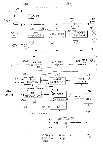
Figure 1 is a schematic block diagram of a digital delay circuit in accordance
with a particular embodiment of the present invention;
Figure 2A is a schematic block diagram of the run control circuit of the
circuit
of Figure 1;
Figure 2B is a schematic circuit diagram of a particular embodiment of the run
control circuit of Figure 2A;
Figure 3A is a schematic block diagram of the oscillator circuit portion of
the
circuit of Figure 1;
Figure 3B is a schematic circuit diagram of a particular embodiment of the
oscillator circuit portion of Figure 3A;
Figure 3C is a circuit diagram of one embodiment of comparator 34e of Figure
3B;
Figure 3D is a circuit diagram of one embodiment of the bias circuit 34s of
Figure 3B;
Figure 4A is a schematic block diagram of a programmable counter in
accordance with a particular embodiment of the counter portion of the circuit
of
Figure 1;
CA 02292542 1999-12-06
WO 98/58228 PCT/US98/12112
-6-
Figure 4B is a schematic diagram of a counter stage and an associated setting
circuit and clearing circuit according to a particular embodiment of the
counter of
Figure 4A;
Figure 4C is a circuit diagram of an alternative embodiment of a setting
circuit
of the programmable counter of Figure 4A;
Figure 5 is a partly cross-sectional perspective view of a transducer-circuit
as-
sembly comprising an electronics module and sleeve together with a transducer
mod-
ule;
Figure 6A is a schematic, partly cross-sectional view showing a delay detona-
for comprising an encapsulated delay circuit in accordance with one embodiment
of
the present invention; and
Figure 6B is a view, enlarged relative to Figure 6A, of the isolation cup and
booster charge components of the detonator of Figure 6A.
DETAILED DESCRIPTION OF THE
INVENTION AND PREFERRED EMBODIMENTS THEREOF
Electronic circuitry in accordance with the present invention comprises an ini-
tiation delay circuit that features one or more of several novel aspects
which, while
they may be employed independently of one another in detonator delay circuits
and in
other circuitry, are preferably combined in a single circuit as described
herein.
A schematic representation of an electronic initiation delay circuit that may
incorporate one or more features of the present invention is provided in
Figure 1. Ini-
tiation delay circuit 10 is powered by a storage capacitor 14 that takes its
charge from
the output of a piezoelectric transducer 12. The piezoelectric transducer 12
is well-
known in the art for producing a pulse of electrical energy in response to a
pressure
pulse that may be delivered by, e.g., a non-electric signal transmission line
such as
detonating cord or shock tube or by a small, near-by charge of explosive
material.
The electrical energy produced by transducer 12 provides an electrical
initiation signal
to delay circuit 10 at input terminal 18a. Most of the energy is stored by
storage ca-
pacitor 14, which thereafter provides electrical energy to power initiation
delay circuit
10 and to activate the electrical initiation element such as semiconductor
bridge
CA 02292542 1999-12-06
WO 98/58228 PCT/US98/12112
_7_
("SCB") 16 connected to circuit 10. Semiconductor bridges are well-known in
the art
for use in initiating detonator output charges.
The transducer and capacitor allow the delay circuit of the present invention
to
be used with non-electric initiation signal lines but, in alternative
embodiments, the
circuit may be connected to an electrical initiation system, i.e., one in
which initiation
signals and, optionally, power, are conveyed to the detonator as electrical
signals
along fuse wires. Non-electric signal transmission lines are preferred over
fuse wires
where it is desired to avoid electromagnetic signal interference from radio
waves,
stray ground currents, lightning, etc. As will be seen, the pressure pulse
that stimu-
lates piezoelectric transducer 12 may comprise an initiation signal from which
the cir-
cuit measures a delay and fires the detonator.
In a typical embodiment, detonator delay circuit 10 is assembled into two ma-
jor components, a triggering portion 18 and a delay portion 28, both of which
com-
prise constituent circuits. Triggering portion 18 may draw power from a power
source, e.g., a storage capacitor 14, and may provide a path through which
capacitor
14 may receive the pulse of electrical energy from piezoelectric transducer
12, e.g.,
via a steering diode 20 that inhibits current flow back to transducer 12.
Preferably,
storage capacitor 14 comprises a 0.5 microfarad capacitor capable of providing
4 mi-
croamps for at least 10 seconds. In an alternative embodiment, triggering
portion 18
may draw power from a battery. Triggering portion 18 provides a controllable
trigger
function that inhibits energy from a power source from initiating the
electrical initia-
tion element until a firing signal is received from the delay portion 28,
indicating that
the desired delay interval has passed. The trigger control function may be
provided
principally via a switching element such as a silicon-controlled rectifier
("SCR") 22
through which the power source, e.g., storage capacitor 14, is connected to
SCB 16.
In the illustrated embodiment, the switching element prevents the discharge of
capaci-
for 14 to output terminal 18b, and thus to SCB 16 until the receipt of a
signal from
trigger control circuit 24. Trigger control circuit 24 pulls SCR 22 into a
conductive
state in response to a triggering signal from delay portion 28 that indicates
that the
desired delay interval has elapsed. Triggering portion 18 preferably also
comprises a
voltage regulator 26 that draws some power from capacitor 14 to provide power
to the
delay portion 28 of detonator delay circuit 10. Triggering portion 18
preferably also
CA 02292542 1999-12-06
WO 98/58228 PCT/US98/12112
_$_
comprises a set voltage circuit 30 that generates an approximate 12 volt
signal desig-
nated PROGP, which is provided to delay portion 28 through input 42c upon
receipt
of an initiation signal. The PROGP signal is used by the delay portion 28, as
dis-
cussed below. Triggering portion I8 is also configured to produce a power
signal
VDD of approximately 5 volts, derived from the power source, upon receipt of
the
initiation signal.
Preferably, triggering portion 18 is fabricated as a dielectrically isolated
bipo-
lar complementary metal oxide silicon (DI BiCMOS) integrated circuit chip
because
such circuitry is well-suited for controlling signals of the magnitude
required to power
the circuit and to reliably fire the initiation element. Delay portion 28 can
be imple-
mented as a standard CMOS (complementary metal oxide silicon) circuit chip.
Preferably, the delay portion 28 is powered from voltage regulator 26 of the
triggering portion 18 through input 42f at a voltage level designated VDD
(usually
about 5 volts) {sometimes referred to herein as "VDD signal"). After a
predetermined
delay following the receipt of the power-up VDD signal at input 42f, delay
portion 28
generates a triggering signal on output pin 42d that is conveyed to the
trigger control
circuit 24 of triggering portion 18 to allow SCR 22 to energize SCB 16.
Preferably,
delay portion 28 comprises several constituent circuits, including a timer
circuit 32 to
measure the delay interval. The timer circuit 32 of delay portion 28 comprises
an
oscillator 34 and a counter 36. Preferably, timer circuit 32 is programmable
and
counter 36 comprises a ripple counter 38 and a program bank 40 that can set
the initial
value of the ripple counter 38. Delay portion 28 preferably also includes a
run control
circuit 46 which, after receiving the PROGP signal, prevents timer circuit 32
from-
being re-initialized after a transient power loss. Delay portion 28 preferably
operates
in two modes: a programming mode in which the delay interval to be counted by
the
circuit is determined, and a delay mode in which it counts the delay interval
upon be-
ing powered up at the VDD voltage level from triggering portion 18. Delay
portion
28 operates in its delay mode unless other particular signals of the proper
voltage are
provided to the run control circuit 46, as discussed below.
As indicated above, one feature of the present invention relates to a run
control
circuit 46 that generates signals which control the power-on reset, run
sequencing and
control of other functions of the detonator delay circuit 10. For example, as
will be
CA 02292542 1999-12-06
WO 98/58228 PCT/US98/12112
_9_
discussed further below, run control circuit 46 will assure that once the
timer circuit
32 has begun counting in the delay mode, it will not be re-initiated after a
transient
power loss. Accordingly, run control circuit 46 will prevent the firing of the
detonator
should a transient power loss threaten the accuracy of the delay interval, as
described
below.
Run control circuit 46 can be understood by reference to the schematic illus-
tration thereof in Figure 2A. Run control circuit 46, in the illustrated
embodiment,
comprises a control power-on reset ("POR") circuit 46a which is responsive to
delay
portion 28 being powered up at the VDD voltage level. POR circuit 46a is also
re-
sponsive to an overnding RESET signal generated by the reset generation
circuit 48
(Figure 1) which is used to program the timer 32 when delay portion 28 is in
its pro-
gramming mode, as described below. POR circuit 46a responds to the VDD signal
and to the overnding RESET signal, as discussed below, by generating a RESET
START signal that is conveyed, for a limited time, to oscillator 34 and to
each stage
I S of a control bank comprising at least three control stages 46b, 46c and
46d. Prefera-
bly, each control stage is configured to have a single data input and two
outputs, i.e.,
normal and inverted outputs. Control stage 46b is referred to as the lock-out
control
stage, control stage 46c is referred to as the counter toad control stage, and
control
stage 46d is referred to as the clock enable control stage. The RESET START
signal
generated by POR circuit 46a clears each of the control stages by setting the
normal
output of each control stage to an inactive or low logic state, and it
initiates the oscil-
lator 34, as will be discussed below. Control stages 46b, 46c and 46d are
connected
together in ripple fashion to carry a signal from one to the next in
accordance with a
clock signal CLK2A provided by the oscillator 34.
Run control circuit 46 further comprises a lock-out switch circuit 46e which
is
configured to receive input signals from lock-out control stage 46b and, from
off chip
sources, a PROGP signal at input 42c (Figure 1 } and a V 18 signal. The PROGP
sig-
nal is received at input 42c after triggering portion 18 receives the electric
initiation
signal and the V 18 input signal, which is used during programming, as
described be-
low. Lock-out switch circuit 46e comprises a lock-out cell (described further
below)
that may have either an active state or an inactive state. The lock-out cell
is non-
volatile, meaning that its state will be preserved even in the event of a loss
of power to
CA 02292542 1999-12-06
WO 98/58228 PCT/US98/12112
-10-
any part of timer circuit 10, and it will only change upon receipt by lock-out
switch
circuit 46e of particular signals, as described herein. For example, lock-out
switch
circuit 46e may comprise a non-volatile, but erasable, electrically
programmable read-
only memory (EEPROM) cell. Lock-out switch circuit 46e is configured so that
when
time delay portion 28 is powered by the VDD signal for the first time after
being pro-
grammed, the lock-out cell will be in the active state and the initial state
of lock-out
signal on line 46g will be active. The two outputs of control stage 46b are
provided to
lock-out switch circuit 46e, as described below, and the normal output of
control stage
46b is additionally provided to the input of counter load stage 46c.
The normal output of counter load control stage 46c is not only connected to
an input of the clock enable control stage 46d, but is also provided as a
counter load
RST signal to the timer, as will be described below. ~ Upon receipt of an
active input
signal from counter load control stage 46c, clock enable control stage 46d
generates
an active output signal on its normal output that is provided as an input to
enable
override circuit 46f, and an inactive output signal RESET START Z on its
inverted
output. The inactive RESET START Z signal releases fire resetting circuit 54
(Figure
1 ), thereby allowing a triggering signal to be provided to triggering portion
18 after
the predetermined delay interval. Enable override circuit 46f receives the
output of
clock enable control stage 46d and, from a source that will be described
below, a sig-
nal designated HV, which is provided when delay portion 28 is placed into its
pro-
gramming mode. Enable override circuit 46f emits a clock enable signal CLKEN
when it receives an active signal from stage 46d, unless it receives an active
HV sig-
nal. Thus, enable overnde circuit 46f is disabled by an active HV signal.
Upon power-up of delay portion 28 in the delay mode, the lock-out signal on
line 46g will be placed in its active state and POR circuit 46a clears control
stages
46b, 46c and 46d, i.e., their normal outputs are inactivated. Once the POR
circuit 46a
times out and the RESET START signal becomes inactive, lock-out control stage
46b
responds to the receipt of a pulse of clock signal CLK2A, i.e., it "clocks",
by generat-
ing a normal output signal Q that follows the logic state of the lock-out
signal on line
46g. This change in the normal output of control stage 46b from inactive to
active
erases the lock-out cell, i.e., puts the cell in the inactive state, but lock-
out switch cir-
cuit 46e will maintain an active lock-out signal on line 46g as long as POR
circuit 46a
CA 02292542 1999-12-06
WO 98/58228 PCT/US98/12112
-11-
does not generate a subsequent RESET START signal. The active normal output of
lock-out control stage 46b on line 46j will, on the next clock pulse, activate
the output
from counter load control stage 46c. The active output from stage 46c provides
the
RST signal and an active input to clock enable control stage 46d. With an
active in-
s put, the next clock pulse will cause stage 46d to provide an active signal
to enable
override circuit 46f on the normal output. Enable override circuit 46f then
produces
the active clock enable signal CLKEN. The active input to clock enable control
stage
46d also causes stage 46d to provide an inactive signal on its inverted
output, i.e., the
RESET START Z signal will now be inactive. As long as the input signal on line
46g
provided to lock-out control stage 46b is active, subsequent clock pulses
CLK2A will
not affect the state of the output from stage 46b. Thus, it can be seen that
the active
RST and CLKEN signals and the inactive RESET START Z signal will continue to
be produced until another RESET START signal clears the control stages, i.e.,
until
the POR circuit 46a is reactivated.
The RST signal and the CLKEN signal may be necessary for the operation of
the detonator delay circuit as will be described below. Since these signals
are derived
from the outputs of ripple-connected stages, it will be understood that they
will not be
produced unless the input to lock-out control stage 46b, which is received
from lock-
out circuit 46e, is in its active state when control stages 46b, 46c and 46d
receive
clock pulses CLK2A after the RESET START signal subsides. However, lock-out
switch circuit 46e is configured so that its ability to generate the active
signal on line
46g upon power-up depends on the active state of the lock-out cell. As
described
above, lock-out control stage 46b causes lock-out switch circuit 46e to erase
the lack-
out cell. Thus, even if a new RESET START signal is received, and control
stages
46b, 46c and 46d are cleared, the RST and CLKEN signals will not be generated,
be-
cause the signal on line 46g is inactive. In other words, control circuit 46
locks out
subsequent operation of timer circuit 10 until the Lock-out cell is
reactivated as de-
scribed herein.
The RST signal produced by run control circuit 46 in normal delay mode op-
eration is conveyed to timer circuit 32 and to fire resetting circuit 54
(Figure 1). The
active RESET START Z signal produced by run control circuit 46 in normal delay
mode operation is conveyed to fire resetting circuit 54 only in response to
the RESET
CA 02292542 2001-O1-15
-12-
START signal, e.g., at power-up. The active RESET START Z signal holds fire
resetting circuit 54 in its reset state so that it cannot enable fire output
circuit 44 to pro-
s vide a triggering signal to triggering portion 18 through output 42d. Fire
resetting circuit
54 is configured so that upon receipt of an inactive RESET START Z signal and
the RST
signal (which are generated after the RESET START signal subsides and control
stages
46b, 46c and 46d receive a seriea of clock pulses from signal CLK2A), it
generates a
signal designated CND that is conveyed to fire output circuit 44 to initialize
that circuit.
Then, upon receipt of a timer output signal from counter 38, the fire output
circuit 44
(Figure 1) will issue the triggering signal on pin 42d.
Inputs for signals V 18 and PROGP to lock-out switch circuit 46e are employed
to by-pass the lock-out function of run control circuit 46, described above,
i.e., to allow
run control circuit 46 to initiate the oscillator 34 and thus enable timer 32
without
locking out subsequent timer functions, for programming purposes, as will be
described
below.
A schematic circuit diagram of a particular implementation of a run control
circuit in accordance with the present invention is shown in Figure 2B. With
reference
to Figure 2B, it can be seen that during normal operation, when the set
voltage circuit 30
(Figure 1 ) generates the PROGf signal (approximately 12 volts) and the POR
circuit 46a
issues the RESET START signal, the program gate of EEPROM cell I49 in lock-out
switch circuit 46e is held low and that the drain of transistor IS 1
determines the state of
the signal on line 46g. Provided that the EEPROM cell I49 was previously
cleared to a
high impedance mode when the delay portion 28 was programmed, the drain of
transistor
I51 will be high, thus providing an active lock-out signal on line 46g to lock-
out control
stage 46b. Later, when the outputs of stage 46b toggle, the gate of transistor
I52 is
driven low. The program gate, comprising transistor I57, which was holding the
program gate of EEPROM cell I49 low, is then released, and EEPROM cell I49 is
allowed to go to a conductive skate. As discussed above, this condition
provides a
permanent" inactive input to control stage 46b upon generation of a RESET
START
signal due to a transient power loss. Future restarts of timer 32 are disabled
because the
drain of transistor I51 will be low and the signal on line 46g will be
inactive. If, due to a
transient power loss resulting from, for example, an intermittent connection
between
capacitor 14 and triggering por~:ion 18 in which a
CA 02292542 1999-12-06
WO 98/58228 PCT/US98/12112
-13-
subsequent RESET START signal is generated by POR circuit 46a, EEPROM cell I49
will not be cleared and the control stages will remain locked out.
The source of the CLK2A signal on which the run control circuit 46 depends
can be any conventional oscillator circuit. The present invention, however,
provides a
S novel oscillator illustrated schematically in Figure 3A. Broadly described,
oscillator
34 operates by providing an RC circuit for the discharge of a charged
capacitor. The
charge carried by the capacitor is monitored by a comparator which generates a
signal
when the capacitor voltage falls below a reference voltage REF, i.e., when the
capaci-
tor becomes discharged. The signal is used by a switching means that
substitutes a
charged capacitor for the discharged capacitor and connects the discharged
capacitor
to the power source that charges it to a voltage that exceeds REF. Typically,
then, the
oscillator comprises two capacitors, although in other embodiments more than
two
capacitors may be employed.
With reference to the embodiment depicted schematically in Figure 3A, the
oscillator 34 comprises a first capacitor 34a and a second capacitor 34b. A
switching
circuit 34c serves to connect one capacitor to an off chip resistor connected
to node
34d through which the capacitor is discharged. The resistor at node 34d is
connected
to the chip at the SETR input 42g (Figure 1). Switching circuit 34c also
connects the
other capacitor to a charging source. In response to a signal received on line
34i, the
switching circuit 34c effectively reverses the position of the two capacitors.
The ca-
pacitor charge, i.e., the charge on the capacitor that is being discharged
through node
34d or a related charge, e.g., the charge on node 34d, is compared to a
reference volt-
age by comparator 34e. When the capacitor charge falls below the reference
volt$ge,
comparator 34e generates a signal that is conveyed to a latch 34f. Upon
receipt of the
comparator signal, latch 34f generates a signal that is taken as the output
signal of the
oscillator on line 34g. The output of latch 34f may also be provided as the
switching
signal to switching circuit 34c, along switch signal line 34i. Thus, as
capacitors 34a
and 34b are alternately charged and discharged, latch 34f will produce a
series of
pulses comprising a clock signal. As indicated in Figure 3A, the clock signal
on line
34g is designated CLK2A, and this is the clock signal that drives the ripple
operation
of run control circuit 46. Figure 3A also illustrates a clock gate 34h that
receives an
output signal from latch 34f but which requires the CLKEN signal from run
control
CA 02292542 1999-12-06
WO 98/58228 PCT/US98/12112
-14-
circuit 46 in order to produce a CLK2 signal corresponding to the clock signal
pro-
duced by latch 34f. The CLK2 signal is used to increment the ripple counter.
To-
gether, the counter and the oscillator comprise a timer, the operation of
which is con-
trolled by run control circuit 46 through clock gate 34h. Without an active
CLKEN
signal, clock gate 34h will not generate the CLK2 signal even though latch 34f
is gen-
erating CLK2A signals for use elsewhere in delay portion 28. Thus, the
operation of
the timer as a whole and, in particular, the operation of the counter in
response to the
clock pulses, depends on the presence of an active CLKEN signal.
The frequency of the oscillator is the frequency with which each output Q, QZ
I0 returns to a given state, e.g., the frequency with which output Q toggles
to the high or
active state. It will be understood by one of ordinary skill in the art that
the resistance
value of the resistor on node 34d will affect the time constant for the
discharge of a
capacitor connected thereto, and that the resistor can be chosen to yield a
desired os-
cillation frequency. The oscillator may have a frequency or period of, e.g.,
about 50
1 S microseconds.
A schematic circuit diagram of a particular implementation of an oscillator
for
use in accordance with the present invention is shown in Figure 3B. Here it
can be
seen that first capacitor 34a and second capacitor 34b are embedded within a
collec-
tion of transistors that comprise switching circuit 34c. Switching circuit 34c
effec-
20 tively connects the discharged capacitor to a power source for recharging
while con-
necting the charged capacitor to a resistor at node 34d to be discharged. It
can also be
seen that the output of latch 34f comprises two outputs Q and QZ, and that the
output
Q controls transistors 34j and 34k via line 34iQ while the output QZ controls
transis-
tors 34m and 34n via line 34iQZ. Together, lines 34iQ and 34iQZ comprise
switch
25 signal line 34i of Figure 3A.
Oscillator 34 (Figure 3B) comprises forced start circuitry comprising charge
control circuit 34p, flip-flop 34q, start-up circuit 34r and bias circuit 34s,
to initiate
the operation of the oscillator at power-up even when a large capacitance is
imposed
on the resistor on node 34d for testing or programming purposes. At power-up,
30 charge control circuit 34p turns on transistors 34t and 34u, thus beginning
the charg-
ing process for capacitors 34a, 34b and overcoming any stray capacitance on
node
34d. When the RESET START signal becomes active, the output of start-up
circuit
CA 02292542 1999-12-06
WO 98/58228 PCT/US98/12112
-15-
34r causes output signal Q of flip-flop 34q to go low, so the "on" signal
provided to
transistors 34t and 34u remains on. Charging continues until the capacitor
voltage
sensed by the comparator 34e at INP exceeds 2/3 VDD. At that point, comparator
34e
switches to a high state, causing output Q of flip-flop 34q, which is
connected to
charge control circuit 34p, to go high. In response, charge control circuit
34p turns off
transistors 34t and 34u. The voltage at the INP input to comparator 34e then
starts to
fall, discharging capacitor 34a through the resistor at node 34d. When INP
falls be-
low 2/3 VDD, the comparator switches to a low state, causing latch 34f to
toggle.
Normal oscillator function then proceeds as described above.
Figure 3C indicates a preferred circuit configuration for comparator 34e,
which embodies a high gain, double-stage, low current draw, fast-switching
circuit.
The bias input signal is current mirrored at M9, M8, M7 and M5. Transistors
M1,
M2, M3 and M4 comprise the first stage of the input differential amplifier and
transis-
tors M 13, M 14, M 15 and M 1 b comprise the second stage.
Figure 3D illustrates a preferred circuit configuration for bias circuit 34s
of
Figure 3B. Transistor b5 ensures that the quad transistor set bl, b2, b3 and
b4 powers
up upon receipt of the RESET START signal. The quad set provides a stable
voltage
source over circuitry variations typical in CMOS manufacturing by taking
advantage
of the differences of threshold voltages between p-type and n-type
transistors. The
remaining transistors in circuit 34s sets the bias of comparator circuit 34e
and limits
the current drawn by the start-up circuit 34r.
The clock signals from oscillator 34 (Figure 3A) can be supplied to any con-
ventional ripple counter that may be programmed to generate a timer output
signal
after counting a specified number of clock pulses. One aspect of the present
inven-
tion, however, relates to a novel programmable counter 36 (Figure 1) that can
be used
in a detonator circuit. Programmable counter 36 comprises a ripple counter 38
that
comprises a plurality of counter stages (such as D-type latches) arranged in
ripple
fashion. Each counter stage 38a, 38b, etc. (Figure 4A), is capable of having
either one
of a "set" state and a "clear" state and comprises inputs by which the state
of the
counter stage can be initialized. Each counter stage comprises at least one
output for
providing a signal that indicates the state of that counter stage. Typically,
the output
is designated Q and each counter stage also provides an inverse output, e.g.,
QZ. Pro-
CA 02292542 2001-O1-15
-16-
grammable counter 36 also comprises a program bank comprising a plurality of
setting
circuits 40a, 40a', etc., and a plurality of clearing circuits 40b, 40b',
etc., there being a
setting circuit and a clearing circuit associated with each counter stage.
Outputs of
setting circuits 40a, 40a', etc., and of clearing circuits 40b, 40bt, etc.,
are connected to
appropriate inputs of the associated counter stage and the setting circuits,
clearing
circuits and counter stages are configured so that an active signal from a
setting circuit
will place the counter stage in the set state and an active signal from the
clearing circuit
will place the counter stage in the clear state. The counter stages are
configured so that
when a clear signal and a set signal are received simultaneously, the signal
of longer
duration will determine the state: of the counter stage. Ripple counter 38 has
an inverting
circuit which inverts the polarity of the PROG signal issued by the PROG
circuit 52
(Figure 1) to generate the VEN signal.
The first counter stage 38a (Figure 4A) receives clock pulses from an
oscillator and
may receive the gated clock signal CLK2 described above with reference to
Figure 2A. The setting circuits have inputs for signals designated VPP, VEN
(from the
PROG circuit 52) and RST; the clearing circuits are provided with inputs for
the RST
signal and a RESET signal from reset generation circuit 48 (Figure 1 ).
Each setting circuit can assume either of two states in which it generates a
set
signal of long or short duration, respectively. The state of the setting
circuit can be 20
fixed by a data signal provided at a suitable data input P. In a preferred
embodiment, an
output signal from the associated counter stage provides the data signal at
data P of the
setting circuit to facilitate a parl:icular programming method described
below.
To facilitate programming, delay portion 28 (Figure 1) comprises a control
input
42a, a power input 42f (for a power signal designated VDD, typically about 5
volts), a
reset generation circuit 48 and a program input 42b (sometimes designated V
18), the
latter being a mufti-function input, as will be explained below.
The procedure for programming the counter schematically illustrated in Figure
4A
is as follows. First, power-up signals of about 5 volts are provided at inputs
42b and 42f
(Figure I) from an external programming device. A logic high or active CONTROL
signal is provided from the external device via input 42a to reset generation
circuit 48.
Reset generation circuit 48 generates a RESET signal which is provided to POR
circuit
46a (Figure 2A) of run control circuit 46 (Figure 1) to override
CA 02292542 1999-12-06
WO 98/58228 PCT/US98/12112
-17-
the internal POR function and reset the entire delay portion 28. When the
CONTROL
signal is drawn low, the POR circuit 46a (Figure 2A) generates a RESET START
sig-
nal that resets the run control stages and activates the oscillator circuit
34. Oscillator
34 begins cycling and drives the control stages of the run control circuit 46.
When
circuit 46f generates the CLKEN signal, clock pulses are released to the
ripple counter
38, which starts to increment. The oscillator 34 and counter 36 are allowed to
cycle
for the desired time interval, at which point the signal at input 42b is
raised above
VDD by at least one volt, i.e., VDD + 1. Preferably, the signal at input 42b
is initially
0.5 volts less than VDD (i.e., VDD - 0.5) and is raised to 2 volts greater
than VDD
(VDD + 2) after the desired time interval has elapsed.
As indicated in Figure 1, input 42b is connected to a V/H circuit 50 which
buffers and distinguishes between various signals from input 42b and generates
ap-
propriate output signals. When the signal at 42b is increased to exceed VDD by
more
than 1 volt at the end of the desired time delay, the V/H circuit produces an
HV signal
that is conveyed to circuit 46f (Figure 2A) of run control circuit 46. Circuit
46f re-
sponds by inactivating the CLKEN signal, thus stopping the timer by preventing
the
oscillator from further incrementing the counter via gate 34h (Figure 3A). VIH
circuit
50 also produces a programming signal VPP whenever the signal at input 42b
exceeds
6 volts. (The effect of the VPP signal will be discussed further below.)
Accordingly,
a signal of at least 0.5 VDD introduced at input 42b will result in the
generation of a
PROG signal. A signal at input 42b that exceeds VDD + 1 will result in the
genera-
tion of an HV signal that stops the counter, and a signal at input 42b that
exceeds 6
volts will result in the generation of a VPP signal. During programming, the
signal-at
input 42a will reach about 14 volts, and lock-out switch circuit 46e (Figure
2A) is
configured so that such a signal resets the lock-out bit thereon.
In view of the function of V/H circuit SO as described above, providing an ini-
tial signal at input 42a of between 0.5 VDD and VDD + 1 concurrently with a
control
signal at input 42a (both of which are connected to reset generation circuit
48) yields a
RESET signal that clears the ripple counter 38 and holds the POR circuit 46a
(Figure
2A) in the reset state. When the CONTROL signal goes low, the internal POR
func-
tion concludes, the oscillator 34 (Figure 1 ) starts, and the counter stages
increment.
After the desired time interval has passed, the signal at input 42a is raised
above VDD
CA 02292542 2001-O1-15
-18-
+ 1, causing V/H circuit 50 to produce the HV signal that stops the counter as
described
above. The signal at input 42b is then increased to a level of at least 6
volts, which
causes V/H circuit 50 to generate the VPP programming signal, which allows the
state of
the setting circuit to be determined by the state of the data signal at the
setting circuit
data input. The high level V 18 signal also resets the lock-out bit in the run
control
circuit 46 to permit subsequent timer function. Thus, by initiating and
terminating the
CONTROL signal and adjustin~; the signal at input 42b appropriately, the power-
up se-
quence and clock operation that occur in normal operation (i.e., as the result
of an input
signal at input 18a that results in a PROGP signal at 42c) can be synchronized
with
measurement of a desired time delay by an external programming device, to
properly
program the timer circuit with t:he desired time delay.
In the illustrated preferred embodiment, the setting circuits receive the
output
signals from the associated counter stages, so that the state of each counter
stage at the
time when the counter is stopped, i.e., at the end of the desired interval, is
reflected by
the state of the associated setting circuit. Preferably, each setting circuit
comprises a
non-volatile circuit element such as an EEPROM cell that is programmed by the
state of
the input data signal to the setting circuit. Accordingly, once the state of
the setting
circuit has been programmed, power can be withdrawn from the timer circuit and
the
configuration of the counter at t:he end of the desired delay will be
retained.
In operation, once the timer has been reset in response to a RESET signal, the
initial states of the counter stages must be loaded from the associated
setting circuits.
This is accomplished when the RST signal is generated by the run control
circuit
illustrated in Figures 2A and 2>=3. The RST signal allows both the setting
circuit and the
clearing circuit associated with each counter stage to convey a signal to the
counter
stage.
The setting circuit and t:he clearing circuit are configured so that after the
RST
signal pulse goes low, they generate their signals to the associated counter
stage
simultaneously but for different time intervals. Generally, the setting
circuits are
configured so that when they are unprogrammed, the time constant for the
setting circuit
is about one-half of the time constant of the clearing circuit. Accordingly,
the clear
signal will be of longer duration than, and will prevail over, the set signal
of an
unprogrammed setting circuit, and the counter stage will be cleared. On the
other hand,
CA 02292542 1999-12-06
WO 98158228 PCTIUS98/12112
-19-
the setting circuits are configured so that, if the non-volatile program
means, e.g., the
EEPROM cell, is programmed, the time constant of the setting circuit is
extended be-
yond the time constant of the clearing circuit, so that after the RST signal
dies, the set
signal will prevail over the clear signal and the counter stage will be set or
"loaded"
with the programming of the setting circuit.
Additional detail for particular embodiments of setting circuits and clearing
circuits for use in a counter according to the present invention is seen in
Figure 4B,
which shows a counter stage 38' with its associated setting circuit 40a" and
associated
clearing circuit 40b". In setting circuit 40a", Q2 indicates the non-volatile
EEPROM
cell.
Once programming is complete, subsequently received signals PROGP and
VDD at inputs 42c and 42f, respectively, will cause POR circuit 46a to
generate a
RESET START signal for the various circuit components of delay portion 28, and
it
causes oscillator 34 to begin functioning. When the PROGP signal and the
initial
I S pulses from oscillator 34 are received by run control circuit 46, 'run
control circuit 46
produces the RST signal, the CLKEN signal, and the RESET START Z signal which
enable other circuits in delay portion 28 to function. At the same time, a
lock-out
portion of run control circuit 46, i.e., lock-out switch circuit 46e, is set
to prevent sub-
sequent operation of the run control sequence. Accordingly, in the event of a
transient
power loss at input 42f after timer operation has begun, the restoration of
power to
input 42f will not result in the reloading of the counter or re-initiation of
the timer be-
cause the non-volatile lock-out cell of run control circuit 46, which was set
prior to the
loss of power, will prevent run control circuit 46 from enabling these
functions. Spe-
cifically, lock-out switch circuit 46e will continue generating an inactive
output signal
despite the loss and re-instatement of power to delay portion 28, and the
inactive sig-
nal received by lock-out control stage 46b will prevent the generation of
active RST
and CLKEN signals. Thus, the delay circuit of the present invention assures
that the
detonator will not fire if a transient power loss occurs during the delay
interval.
In an alternative embodiment of a programmable electronic timer circuit in
accordance with this invention, the non-volatile program means of the setting
circuit
may comprise a fusible link instead of an EEPROM cell. A circuit diagram for
such a
setting circuit is shown in Figure 4C. Setting circuit 140a" has the inputs
for the same
CA 02292542 1999-12-06
WO 98/58228 PCTIUS98/12112
-20-
signals as setting circuit 40a" of Figure 4B, i.e., VEN, VPP, RST, data (Q),
and gen-
erates the same output signal, SDN (set). The programming of setting circuit
140a",
and the loading of an associated counter stage therefrom is accomplished in
generally
the same way as for setting circuits comprising EEPROM cells. However, the pro-
s gramming procedure results either in leaving the fusible link 142 intact, or
in causing
it to open. Specifically, when an active signal from the corresponding counter
stage is
received on the data input during the programming process, fusible link 142
remains
intact. Subsequently, when the settings of the program bank are loaded into
the
counter, the intact fusible link effectively short-circuits the output signal
of setting
circuit 140a". Accordingly, the clearing signal from the clearing circuit
outlasts the
setting signal from the setting circuit, and the corresponding counter stage
is cleared.
Conversely, when an inactive signal or "zero" is received at the data input
during pro-
gramming, the fusible link is opened. When the associated counter stage is
later
loaded, setting circuit 140a" is able to produce a setting signal (SDN) that
outlasts the
clearing signal from the associated clearing circuit, and the counter stage
will then he
set.
Typically, more current is required to open a fusible link than to set an
EEPROM cell. Accordingly, setting circuit 140a" has a somewhat different
configu-
ration than setting circuit 40a" of Figure 4B. For example, circuit elements
I12 and
I14 of setting circuit 140x" are larger than corresponding elements of circuit
40a" such
as QI and Q4, so that they can handle sufficient current to open the fusible
link at volt-
ages consistent with CMOS circuitry.
An alternative programming method would be to trim (i.e., open) the appro-.
priate fusible links using a laser instead of running the counter for a
desired time in
terval and using the output signals from counter stages to control fuse-
opening cur
rents. In this alternative approach, more reliance is placed upon the accuracy
of the
oscillator frequency than in the previously described programming method. In
the
previously described method, the circuit is allowed to run for a period of
time meas-
ured against an external known clock, and when the desired interval is
reached, the
counter is stopped and the program bank is programmed according to the output
sig-
nals of the counter stages. Thus, all the timers will measure the interval
counted by
the external clock even if oscillator frequencies (and therefore the program
counts)
CA 02292542 1999-12-06
WO 98/58228 PCTIUS98/12112
-21-
vary from chip to chip. The trimming method, however, is insensitive to
variations in
oscillator frequency and can only establish a known delay if the oscillator
frequency is
known in advance. Therefore, the trimming method requires greater precision in
os-
cillator manufacture.
While, in the embodiment of Figure 1, delay portion 28 is used in connection
with a triggering portion 18 to control the firing of an SCB for the
initiation of a deto-
nator, the triggering signal produced by delay portion 28 can be used to
control any
device that must operate within a predetermined time interval from the receipt
of the
initiation signals provided to delay portion 28.
I 0 Similarly, programmable timer circuit 32 can be used in devices other than
detonators wherever an electronically programmable and non-volatile timer is
needed.
Likewise, oscillator 34, which is advantageously employed as part of a timer,
can be
used as part of any other device requiring a clock pulse.
An electronic delay circuit in accordance with the present invention can be in-
I 5 corporated into a transducer-circuit assembly generally shown in Figure 5
for conven-
Tent incorporation into a detonator. Transducer-circuit assembly 155 comprises
an
electronics module 154 that comprises the delay circuit 10 of Figure 1 with an
initia-
tion element 146 (e.g., an SCB) attached thereto. Figure 5 shows various
components
of delay circuit 10, including delay portion 28 with an associated resistor
134d
20 (attached to node 34d, Figure 3A), a triggering portion 18, a storage
capacitor 14, an
optional bleed resistor I 16 (for slowly discharging capacitor 14 should the
detonator
fail to fire after capacitor 14 is charged, in embodiments that do not include
the lock-
out feature described above) and output leads 137 that provide an output
terminal to
which storage capacitor 14 is discharged. These various components are mounted
on
25 lattice-like portions or traces 141 of a lead frame and, except for output
leads (or out-
put "terminal") 137, are disposed within an encapsulation 115. The transducer-
circuit
assembly 155 comprises initiation element 146 which comprises semiconductor
bridge 16 (which is connected across output leads 137), an initiation charge
146a,
which preferably comprises a fine particulate explosive material such as BNCP
30 (tetraammine-cis-bis (5-nitro-2H-tetrazolato-NZ) cobalt (III) perchlorate),
DXN-l,
DDNP, lead azide or lead styphnate, in an initiation shell 146b that is
crimped onto
neck region 144 of encapsulation 115 and which holds initiation charge 146a in
en-
CA 02292542 1999-12-06
WO 98/58228 PCT/US98/12112
-22-
ergy transfer relation to semiconductor bridge 16. Initiation charge 146a is
preferably
pressed into initiation shell 146b to a density of less than 80 percent of its
theoretical
maximum density (TMD). For example, the initiation unit may be pressed into
shell
146b at a pressure of about 1,000 psi. Preferably, SCB 16 is secured to output
leads
137 in a manner that allows SCB 16 to protrude into, and to be surrounded by,
initia-
tion charge 146a. Alternatively, such materials may be rendered in the form of
a
slurry or bead mix that can be applied onto the SCB. Output initiation element
146
may comprise part of the output means of a detonator and may be used, e.g., to
initiate
the base charge or "output" charge of the detonator in which transducer-
circuit as-
sembly 155 is disposed, as described below.
Encapsulation 11 S preferably engages a sleeve 121 only along longitudinally
extending protuberant ridges or fins (which are not visible in Figure 5) and
thus es-
tablishes a gap 148 between encapsulation 115 and sleeve 121 at the
circumferential
regions about encapsulation 115 between the fins. (Alternatively,
encapsulation 115
may comprise a shock-absorbing material that may optionally make full contact
with
sleeve 121.) Encapsulation 115 optionally defines scallops 150 that make test
leads
152 accessible but which preferably allow the leads to remain within the
surface pro-
file of encapsulation 115, i.e., the leads preferably do not extend into gap
148. If
scallops 150 are omitted, it is preferred that the test leads do not extend
across gap
148 to contact the surrounding enclosure. Accordingly, before the electronics
module,
which comprises the various circuit elements, output initiation element 146
and en-
capsulation 115, is placed within sleeve 121, leads such as leads 152 can be
accessed
to test the assembled circuitry. Then, electronics module 154 can be inserted
into-
sleeve 121 and leads 152 will not contact sleeve 121.
Electronics module 154 is designed so that output leads 137 and initiation in-
put leads 156, through which storage capacitor 14 can be charged, protrude
from re-
spective opposite ends of electronics module 154. A transducer module 158 com-
prises a piezoelectric transducer 12 and two transfer leads 162 enclosed
within trans-
ducer encapsulation 164. Transducer encapsulation 164 is dimensioned and
config-
ured to engage sleeve 121 so that transducer module 158 can be secured onto
the end
of sleeve 121 with leads 162 in contact with input leads 156. Preferably,
encapsula-
tion 11 S, sleeve 121 and transducer encapsulation 164 are dimensioned and
config-
CA 02292542 1999-12-06
WO 98/58228 PCT/US98I12112
-23-
cared so that, when assembled as shown in Figure 5, an air gap indicated at
166 is es-
tablished between encapsulation 115 and transducer encapsulation 164. In this
way,
electronics module 154 is at least partially shielded from the detonation
shock wave
that causes piezoelectric transducer 12 to create the electrical pulse that
initiates elec-
tronics module 154. The pressure imposed by such detonation shock wave is
trans-
ferred through transducer module 158 onto sleeve 121, as indicated by force
arrows
168, rather than onto electronics module 154. The various circuit packages and
ele-
ments may be mounted directly on the metal traces 141 of a lead frame or,
alterna-
tively, on a polymeric or ceramic substrate in a chip-on-board type
arrangement.
Referring now to Figure 6A, there is shown one embodiment of a delay deto-
nator 200 comprising an electronics module in accordance with the present
invention.
Delay detonator 200 comprises a housing 212 that has an open end 212a and a
closed
end 212b. Housing 212 is made of an electrically conductive material, usually
alumi-
num, and is preferably the size and shape of conventional blasting caps, i.e.,
detona-
toys. Detonator 200 comprises an initiation signal transmission means for
delivering
an electrical initiation signal to the delay circuit. As indicated above, the
initiation
signal transmission means may simply comprise fuse wires connected to input
termi-
nals of the delay circuit. Preferably, however, the detonator is used as part
of a non-
electrical system and the initiation signal transmission means comprises the
end of a
non-electric signal transmission line (e.g., shock tube) and a transducer for
converting
the non-electric initiation signal to an electrical signal, as described
herein. In the il-
lustrated embodiment, the delay detonator 200 is coupled to a non-electric
initiation
signal means that comprises, in the illustrated case, a shock tube 2i0,
booster charge
220 and transducer module 158. It will be understood that non-electric signal
trans-
mission lines besides shock tube, such as a detonating cord, low-energy
detonating
cord, low velocity shock tube and the like may be used. As is well-known to
those
skilled in the art, shock tube comprises hollow plastic tubing, the inside
wall of which
is coated with an explosive material so that, upon ignition, a low-energy
shock wave
is propagated through the tube. See, for example, Thureson et al U.S. Patent
4,607,573, issued August 26, 1986. Shock tube 210 is secured in housing 212 by
an
adapter bushing 214 that surrounds tube 210. Housing 212 is crimped onto
bushing
214 at crimps 216, 216a to secure shock tube 210 in housing 212 and to form an
envi-
CA 02292542 1999-12-06
WO 98158228 PCT/US98/12112
-24-
ronmentally protective seal between housing 212 and the outer surface of shock
tube
210. A segment 210a of shock tube 210 extends within housing 2I2 and
terminates at
end 210b in close proximity to, or in abutting contact with, an anti-static
isolation cup
218.
Isolation cup 218 has a friction fit inside housing 212 and is made of a semi-
conductive material, e.g., a carbon-filled polymeric material, so that it
forms a con-
ductive grounding path from shock tube 210 to housing 212 to dissipate any
static
electricity which may travel along shock tube 210. Such isolation cups are
well-
known in the art. See, e.g., U.S. Patent 3,981,240 to Gladden, issued
September 21,
1976. A low-energy booster charge 220 is positioned adjacent to anti-static
isolation
cup 218. As best seen in Figure 6B, anti-static isolation cup 218 comprises,
as is
well-known in the art, a generally cylindrical body (which is usually in the
form of a
truncated cone, with the larger diameter end disposed towards the open end
212a of
housing 212) which is divided by a thin, rupturable membrane 218b into an
entry
chamber 218a and an exit chamber 218c. The end 210b of shock tube 210 (Figure
6A) is received within entry chamber 218a (shock tube 210 is not shown in
Figure 6B
for clarity of illustration). Exit chamber 218c provides an air space or stand-
off be-
tween the end 210b of shock tube 210 and booster charge 220 which are disposed
in
mutual signal transfer relation to each other. In operation, the shock wave
signal
emitted from end 210b of shock tube 210 will rupture membrane 218b, traverse
the
stand-off provided by exit chamber 218c and initiate booster charge 220.
Booster charge 220 comprises a small quantity of a primary explosive 224
such as lead azide (or a suitable secondary explosive material such as BNCP),
which.
is disposed within a booster shell 232 and upon which is disposed a first
cushion ele-
ment 226 (not shown in Figure 6A for ease of illustration). First cushion
element 226,
which is annular in configuration except for a thin central membrane, is
located be-
tween isolation cup 2 l 8 and explosive 224, and serves to protect explosive
224 from
pressure imposed upon it during manufacture.
Isolation cup 218, first cushion element 226, and booster charge 220 may con-
veniently be fitted into a booster shell 232 as shown in Figure 6B. The outer
surface
of isolation cup 218 is in conductive contact with the inner surface of
booster shell
232 which in turn is in conductive contact with housing 212 to provide an
electrical
CA 02292542 1999-12-06
WO 98/58228 PCT/US98/12112
-25-
current path for any static electricity discharged from shock tube 210.
Generally,
booster shell 232 is inserted into housing 212 and housing 212 is crimped to
retain
booster shell 232 therein as well as to protect the contents of housing 212
from the
environment.
A non-conductive buffer 228 (not shown in Figure 6A for ease of illustration),
which is typically 0.015 inch thick, is located between booster charge 220 and
trans-
ducer module 158 to electrically isolate transducer module 158 from booster
charge
220. Transducer module 158 comprises a piezoelectric transducer (not shown in
Fig-
ure 6A) that is disposed in force-communicating relationship with booster
charge 220
I O and so can convert the output force of booster charge 220 to a pulse of
electrical en-
ergy. Transducer module 158 is operatively connected to electronics module 154
as
shown in Figure 5. The initiation signal transmission means comprising shock
tube
segment 210a, booster charge 220 and transducer module 158 serves to deliver
to de-
lay circuit 10, in electrical form, a non-electric initiation signal received
via shock
tube 210, as described below.
The enclosure for the initiation and output charges provided by detonator 200
comprises, in addition to housing 212, the optional open-ended steel sleeve
121 that
encloses electronics module 154. Electronics module 154 comprises at its
output end
an output initiation element 146 (shown in Figure 5), which comprises part of
the out-
put means for the detonator. Adjacent to the initiation element of electronics
module
154 is a second cushion element 242, which is similar to first cushion element
226.
Second cushion element 242 separates the output end of electronics module 154
from
the remainder of the detonator output means, comprising an output charge 244
that is.
pressed into the closed end 212b of housing 212. Output charge 244 comprises a
sec-
ondary explosive 244b that is sensitive to the initiation element of
electronics module
154 and that has sufficient shock power to detonate cast booster explosives,
dynamite,
etc. Output charge 244 may optionally comprise a relatively small charge of a
pri-
mary explosive 244a for initiating secondary explosive 244b, but primary
explosive
244a may be omitted if the initiation charge of electronics module 154 has
sufficient
output strength to initiate secondary explosive 244b. The secondary explosive
244b
has sufficient shock power to rupture housing 212 and detonate cast booster
explo-
sives, dynamite, etc., disposed in signal transfer proximity to detonator 200.
The out-
CA 02292542 1999-12-06
WO 98/58228 PCTIUS98/12I12
-26-
put means for the detonator comprises those components, including reactive
materials,
e.g., explosives, that are initiated by the discharge of the storage means to
the output
terminal. Thus, in the embodiment illustrated in Figures 5, 6A and 6B, the
detonator
output means comprises the initiation element 146, initiation charge 146a and
output
charge 244.
In use, a non-electric initiation signal traveling through shock tube 210 is
emitted at end 210b. The signal ruptures membrane 218b of isolation cup 2I8
and
first cushion element 226 to activate booster charge 220 by initiating primary
explo-
sive 224. Primary explosive 224 generates a detonation shock wave that imposes
an
output force on the piezoelectric generator in transducer module 158. The
piezoelec-
tric generator is in force-communicating relationship with booster charge 220
and so
converts the output force to an electrical output signal in the form of a
pulse of electri-
cal energy that is received by electronics module 154. As indicated above,
electronics
module 154 stores the pulse of electric energy and, after a predetermined
delay, re-
leases or conveys the energy to the detonator output means. In the illustrated
em-
bodiment, the charge is released to the initiation element, which initiates
output
charge 244. Output charge 244 ruptures housing 212 and emits an explosive
output
signal that can be used to initiate other explosive devices, as is well-known
in the art.
While the invention has been described in detail with reference to a
particular
embodiment thereof, it will be apparent that upon a reading and understanding
of the
foregoing, numerous alterations to the described embodiment will occur to
those
skilled in the art and it is intended to include such alterations within the
scope of the
appended claims.