Note : Les descriptions sont présentées dans la langue officielle dans laquelle elles ont été soumises.
CA 02294188 2006-03-30
1
CALIBRATION SYSTEM FOR A PHOTOMULTIPLIER TUBE
BACKGROUND
The following relates to an optical system and its
method of operation.
Today, a number of machines, such as medical analyzers
and the like, operate or otherwise perform their functions
by looking at or reading a signal. In some cases, this
signal may be a light signal generated by a particular
marker or label attached to an item of interest. In order
to read this light signal, these machines may use an
optical system which gathers the light signal and guides
the gathered light signal to a reader, such as an element
that produces an electrical signal in response to the
gathered and guided light signal.
For such machines to operate as intended, it is
desirable to check or to calibrate the optical system from
time to time. Depending on the type of machine involved,
this checking may be rather difficult. Also, the method or
device used to check the optical system may not always
accurately check the optical system. Accordingly, it is
desirable to provide an improved optical system.
Si7bIlMARY
Optical systems are provided. In one embodiment, the
optical system includes a detector for detecting a light
signal. A light signal gatherer and guider is optically
connected with the detector for gathering the light signal
and guiding the light signal to the detector. The light
signal gatherer and guider has a check signal entrance
location disposed along an outer surface of the light
signal gatherer and guider. A check signal source is
optically connected with the light signal gatherer and
guider so that a check signal generated by the check signal
source randomly illuminates the check signal entrance
location on the outer surface of the light signal gatherer
and guider.
CA 02294188 2006-03-30
2
In accordance with the invention, there is provided an
optical system comprising:
(a) a detector for detecting a light signal;
(b) a light signal gatherer and guider optically
connected with the detector (a) for gathering the light
signal and guiding the light signal to the detector (a),
the light signal gatherer and guider (b) having an outer
surface and an end;
(c) a check signal entrance location disposed along
the outer surface of the light signal gatherer and guider
(b) ;
(d) a check signal source optically connected with
the light signal gatherer and guider (b) so that a check
signal generated by the check signal source (c) randomly
illuminates the check signal entrance location on the outer
surface of the light signal gatherer and guider (b), and
(e) a diffuser optically located between the check
signal source (d) and the light signal gatherer and guider
(b).
BRIEF DESCRIPTION OF DRAWINGS
FIG. 1 is a cut-away view of an optical system
described herein;
FIG. 2 is spectral distribution of acridinium;
FIG. 3 is a representation of an image pattern of an
element optical system of FIG. 1;
FIG. 4 is a schematic diagram of a portion of the
optical system of FIG. 1;
FIG. 5 is a polar plot of a frequency response around
a feedback loop comprising the optical system of FIG. 1;
FIGS. 6 and 7 show magnitude and phase response,
respectively, of a transfer function using Bode plots; and
FIG. 8 represents transient response of the optical
system of FIG. 1 with respect to a step input.
DETAILED DESCRIPTION OF ILLUSTRATED EMBODIMENTS
One embodiment of an optical system 20 is illustrated
in FIG. 1. For the sake of clarity of understanding, the
CA 02294188 2006-03-30
3
optical system 20 will be discussed with respect to a
particular utilization or employment. For instance, the
optical system 20 may be used with the constructions
disclosed in U. S. Patent 5,856,194, Arnquist et al, issued
January 5, 1999, assigned to Abbott Laboratories. It is to
be noted, however, that the optical system 20, possibly
with suitable modifications, may be used in other
employments without departing from the scope of the
appended claims.
For the purposes of this discussion, the optical
system 20 is used to quantitatively detect light emitted
from a label, such as lumophore molecules, for example,
that have been tagged to conjugate molecules which, in
turn, have been constructed to react with a specific item
of interest or analyte molecules in a sample. Luminescence
or generation of a light signal is achieved through
addition of an activator reagent (sometimes referred to as
a"trigger") and subsequent chemical reaction with any
lumophore tagged molecules present in a container, such as
a reaction vessel. The luminescent light or light signal
produced during such a reaction may be directly or
indirectly proportional to an amount of analyte present in
the sample, depending on the type of assay or determination
of item of interest in the sample.
Detection of the light signal may be accomplished by
using a photon counting module to measure chemical
luminescence. The photon counting module, in one
embodiment, may comprise a detector, such as an end window
photomultiplier tube and the like, operated in a photon
counting mode and an optical performance check signal
source, such as a blue light emitting diode and the like.
The photomultiplier tube is optically connected to the
reaction vessel in a read chamber by means of a light
signal collector and guide, such as a fused quartz light
CA 02294188 1999-12-14
WO 99/09381 PCT/US98/17047
4
pipe and the like. In a particular employment, once the
reaction vessel enters the read chamber, a shutter closes around
the reaction vessel to block ambient or environmental light. A
magnet removes magnetic particles from suspension, and trigger
reagent is added to initiate the luminescent reaction or
generation of the light signal.
Performance of the optical system may be determined using a
dilution series of label, for instance, acridinium amide,
standards. Relative light units are measured over the photon
counting module's dynamic range, which may be substantially
within the range of about several million to less than about 20,
after dark count subtraction. Both low end photon counting
.module sensitivity and high end linearity may be quantitated for
a given population of optical systems and may be compared to
similar parameters for immunoassays requiring a low level of
analyte detection and a wide calibration dynamic range.
Each photon counting module may be calibrated against a
standard to correct for gain and linearity variations. Multiple
data points are taken using a photon reference that closely
matches a spectral distribution of the label, i.e. an acridinium
and the like. These data points may be used to normalize a
response against the standard and to determine a required
linearity correction parameter.
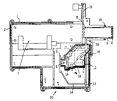
Figure 1 illustrates an exemplary construction of an
embodiment of an optical system 20. In this embodiment,
components of the optical system 20 are located in a housing 1,
which may be made of an injection molded polymer and the like.
The housing 1 incorporates a labyrinth seal 2 at its outer
perimeter. The seal 2 maintains substantially light tight
conditions within the interior of the housing 1.
The housing 1 includes an internal chamber 3, also bounded
by a labyrinth seal 4. The internal chamber 3 houses elements
which direct light, shown in dotted lines in Figure 1, from a
calibration signal source or check signal source 5, which may be
a blue light emitting diode and the like. The check signal
source 5 may be mounted on a printed circuit board 6 to
facilitate assembly of the optical system 20.
tl
CA 02294188 1999-12-14
WO 99/09381 PGT/US98/17047
A photon counting module 7 comprises a photomultiplier
tube, a photomultiplier tube socket, a voltage divider circuit,
a high voltage power supply, a high gain AC amplifier, a
discriminator, a reference voltage, a pulse shaper and a
prescaler, not shown in Figure 1 for clarity. Output from the
prescaler is connected to a high speed digital counter which is
used to count a number of photon pulses. Light, such as light
from the check source 5, light signal emissions from a sample in
a reaction vessel, etc., are gathered and guided to the
photomultiplier tube by a light gatherer and guider or light
pipe 8. The light pipe 8 is maintained in a desired orientation
by an end cap 9 which contains seals 10 and 11. The seals 10
and 11 reduce the likelihood that liquids or other contaminates
might enter the housing 1.
In an exemplary embodiment, the photon counting module 7
may be Part Number: P30CWAD5-07 available from THORN EMI
Electron Tubes Ltd. of Middlesex, England. The light pipe 8 is
available from Collomated Holes, Inc. of Campbell, California.
The check source 5 may be Part Number: NLPB300A from Nichia
Chemical Industries, LTD. of Tokushima, JAPAN.
Intensity of the check source 5 is adjusted by using a
silicon photodiode 12 and analog electronics disposed on a
printed circuit board 13. In a particular embodiment, the
photodiode 12 may be Part Number: OPT301M available from Burr-
Brown Corporation of Tucson, Arizona.
A conductor 14 is routed from the analog electronics board
13 to a check source 5 operating board 6 to supply power to the
check source 5 and form a closed loop control system for the
check source 5. The light output of the check source 5 is
scattered using diffuser 15 to create a lambertian source. in a
particular embodiment, the material comprising the diffuser 15
may be 500 grit ground glass and the like. Alternate materials,
such as opal glass and the like, may also be used. In a
specific embodiment, the diffuser 15 may be Part Number: 55.3000
available from Rolyn Optics Company of Covina, California.
The scattering provided by the diffuser 15 decreases
optical system 20 sensitivity to position between the check
CA 02294188 1999-12-14
WO 99/09381 PCT/US98/17047
6
source 5 image and the silicon photodiode 12. This scattering
creates a system of random illumination across the surface of
the light pipe 8 at the check source 5 signal entrance location
30 and therefore makes the optical system 20 tolerant to
manufacturing variations. The check source 5 signal is not
focused onto the light pipe 8, rather the check source 5 signal
randomly illuminates a portion outer surface area of the light
pipe 8 at the entrance location 30.
Light exiting the diffuser 15 illuminates the silicon
photodiode 12 after passing through a first glass plate 16.
This first glass plate 16 acts as a beam splitter and is offset
at an angle measuring about 45 degrees with respect to a line
intersecting the check source 5 and the photodiode 12. Light
striking the silicon photodiode 12 produces a photocurrent
proportional to an adjustable reference voltage on the analog
electronics board 13.
A portion of the light striking the first glass plate 16 is
reflected toward a second glass plate 17 also offset at an angle
measuring about 45 degrees. The second glass plate 17 reflects
a portion of the light striking the second glass plate 17 toward
a third glass plate 18 offset at an angle measuring about 45
degrees. After striking the third glass plate 18, the light
reflected from the surface of the third glass plate 18 is
optically coupled to a side of the light pipe 8 at the entrance
location 30. The area of illumination that subtends the light
pipe 8 at the entrance location 30 is, in an exemplary
embodiment, approximately 0.076 square inches. The entrance
location 30 is positioned along a portion of a circumference of
the light pipe 8 such that the check source 5 signal enters the
light pipe 8 at the entrance location 30 substantially along a
radius or at the side of the light pipe 8. It is to be noted
that the check source 5 signal does not enter the light pipe
substantially along an axis or at an end of the light pipe 8.
The light striking the side of the light pipe 8 is
optically coupled, i.e. gathered and guided, into the
photomultiplier tube for checking performance of the photon
counting module 7. A shutter mechanism 19 may be provided to
CA 02294188 1999-12-14
WO 99/09381 PCT/US98/17047
7
protect a photocathode of the photomultiplier tube from direct
exposure to ambient light during installation, removal,
cleaning, etc. of the light pipe 8.
In'a specific embodiment, a gallium nitride blue light
emitting diode was selected as the check source 5 because its
output closely or substantially matches the spectral
distribution of acridinium, which is shown in Figure 2. By
substantially matching the output of the check source 5 with the
spectral distribution of a given marker to be used with the
optical system 20, a probability of generating errors in optical
system 20 normalization due to varying spectral responses of
various photomultiplier tubes is reduced. Put more generally,
the check source 5 may be chosen such that the check signal
generated by the check source 5 is substantially matches, in
relevant aspects, the light signal to be detected by the
detector (photomultiplier tube) comprising the optical system
20.
An image of the check source 5 has a pattern substantially
similar to that shown in Figure 3. The pattern comprises rings
of varying intensity 21 and 22 and a center 23 of an image of
the check source 5. This pattern can shift across the surface
of the silicon photodiode 12 due to variations in, e.g., check
source 5 construction, check source 5 positioning, photodiode 12
positioning, and glass plate 16 (beam splitter) tolerances, etc.
These variations may effect photodiode 12 response. Photodiode
12 response variations, in turn, can contribute to a significant
control response difference from one optical system 20 to
another.
To reduce an effect of such variations, the diffuser 15 is
placed in front of the check source 5. Light that strikes the
diffuser 15 is scattered in all directions, thereby appearing to
have substantially the same brightness when viewed at any angle.
A perfect diffuser, or lambertian source, will have a brightness
at any angle whose radiation per unit area is defined by Io cos
q, where Io is the intensity of an element of area in a
direction perpendicular to the surface and q is the angle to the
CA 02294188 1999-12-14
WO 99/09381 PCT/US98/17047
8
surface normal. The partial diffusion properties of the
diffuser 15 are sufficient to provide an effective lambertian
source of light.
Light exiting the diffuser 15 strikes the first glass plate
16, offset at an angle of about 45 degrees, which acts as a beam
splitter, thereby separating the incident light beam from one
beam into two. A portion of the light is transmitted through
the first glass plate 16 and a portion is reflected. The
portion of the light which is reflected from the surface of the
first glass plate 16 is given by the Fresnel reflection equation
below:
R- I sin2 (I- I') + tan2
2 sin I') t ;2(1+ I')
where I and I' are the angles of incidence and refraction.
For the optical system 20, I= 45 degrees and I' = 27.7
degrees. Using the above equation yields a reflection value of
approximately 5.3%. Therefore, the amount of energy transmitted
to the photodiode 12 is given by the equation T = 1 - R or
94.7%. Allowing a majority of the energy to be transmitted to
the photodiode 12 serves three main purposes:
11 Allows enough energy to pass to the photodiode 12 so
the signal-to-noise ratio of the photodiode 12 is not
significant.
2] Allows the gain of a transimpedance amplifier to be a
reasonable value.
3] Provides a method of attenuating the light to a level
which is acceptable to the photon counting module 7.
The multiple glass plates, three in this embodiment,
provide a means of steering the light beam from the check source
to the light pipe 8. However, the multiple glass plates 16,
17 and 18 attenuate the light emitted by the check source 5 to a
CA 02294188 1999-12-14
WO 99/09381 PCT/US98/17047
9
level acceptable to the photon counting module 7. At the
wavelengths of interest, each glass plate 16, 17 and 18 can be
treated as having a substantially uniform spectral transmission
(neutral density) with an optical density (O.D.) given per the
following formula:
O.D.=1og[2]
where T is the amount of reflected energy.
In a particular embodiment, each glass plate 16, 17 and 18
then has an O.D. value of approximately 1.276. The diffuser 15
has a total transmission of approximately 70% which equates to
an O.D. value of about 0.155. An approximation of the effective
total density of the optical system 20 can be given as the sum
of the individual densities. Therefore, the optical system 20
O.D. is approximately 3.983 from the check source 5 to the light
pipe 8. This means is that only about 0.01% of the light from
the check source 5 strikes the side of the light pipe 8 at the
entrance location 30.
The light striking the side of the light pipe 8 can be
treated as skew rays. These skew rays rotate with each
reflection with the amount of rotation being dependent on the
entrance position and angle. A portion of the light will
eventually emerge from the end of the light pipe 8 closest to
the photomultiplier tube.
The electronics used to control the check source 5 are
shown in Figure 4. Input power and control signals to the
analog electronics board 13 come in through connector Jl,
indicated by reference character 24, on the printed circuit
board 13. The circuit requires +12Vdc, -12Vdc and ground for
power with a 16-bit Digital-to-Analog Converter (DAC) 25 with
serial data interface requiring the following additional lines:
Clear, Serial Data Clock and Serial Data Input signals. The
output of the DAC 25 is used as a reference voltage to control
the intensity of the check source 5 and is operated in the
bipolar mode with an output range of -5Vdc to +5Vdc. The
CA 02294188 1999-12-14
WO 99/09381 PCT/US98/17047
bipolar mode was chosen to provide a method of turning the check
source 5 off completely because of the offset voltages and
currents of the various components in the circuit. This method
reduces a need to manually adjust the circuit using, for
instance, potentiometers.
In an exemplary embodiment, the silicon photodiode 12 is an
opto-electronic device containing a photodiode and
transimpedance amplifier on a single chip 26. The photodiode
12 current is wavelength dependent, is defined as the
responsivity in amperes/watt (A/W), and is proportional to the
radiant power (watts) falling on the photodiode 12. Therefore,
the final photodiode 12 current becomes a convolution between
the spectral output of the check source 5 and the responsivity
of the photodiode 12. Selected as a balance between signal-to-
noise ratio, signal bandwidth and elimination of any special
board design or handling requirements, the transimpedance
amplifier has a gain of about 30 x 106. The dynamic range of
the reference voltage can be adjusted by connecting a power
supply to the check source 5 current limiting resistor 27 and
varying the voltage so a count value at the upper range of
linearity for the photon counting module 7 is achieved.
The resolution of the reference voltage, or Least
Significant Bit (LSB), due to the DAC 25, can be calculated as
follows:
LSB = OutputVolt ageRange - 10 V = 153 V [3)
2Numberoi ts - 2717
The final resolution of the reference voltage used to control
the check source 5 intensity is adjusted using resistors RA and
RB (Figure 4) :
LSBFina1= LSB* R R R = ]139v [4]
A B
CA 02294188 1999-12-14
WO 99/09381 PCT/US98/17047
11
This reduces the dynamic range of the reference voltage to
substantially within the range of -454mV to +454mV. The output
of the transimpedance amplifier and the reference voltage are
applied to differential DC amplifier 28. Assuming ideal
conditions and noting that R1/R8 = R6/R2, the output voltage
reduces to
Vl-[R8]*(VT-VR) [5]
The output of the differential DC amplifier 28 is applied to
noninverting amplifier 29. Again, assuming ideal conditions,
the output voltage becomes:
V2 1+ ~] *(V1) [6]
Combining these two equations yields the voltage that drives the
check source 5:
V2 =~1+RS]*[R8]*(VT_VR~ [7]
The voltage of the transimpedance amplifier is:
VT= R3*Iphotod;ode [8]
where, because of output scaling,
I V [9]
ph c di de R 3
therefore, the transimpedance output is equal to the voltage
driving the check source 5,
VT=V2 [10]
CA 02294188 1999-12-14
WO 99/09381 PCT/US98/17047
12
Inserting this relationship into equation [7] above and solving
for V2 shows the relationship between the reference voltage and
check source 5 drive voltage:
V2 VR
=
1 [11]
1+ R4 * R1
I RS R8
At low frequencies, where loop gain is high, the closed loop
gain is determined by the feedback network. Equation [11] shows
that the drive voltage to the check source 5 is equal to the
reference voltage when the gain of the feedback network is
large. Solving equation [11] yields:
V2 =1.00001 VR [121
At low frequencies, the fractional part in the denominator
approximates the gain error. For this system, the fractional
part is substantially equal to about 100,100 or 100dB, which
equates to a gain error of approximately 0.001%.
Table 1 shows the spice pole/zero analysis of the closed
loop system.
CA 02294188 1999-12-14
WO 99/09381 13 PCT/US98/17047
TABLE 1
Spice Plus Version 3.1.6
CIRCUIT NAME: OPA627 - START OF DECK
PZ analysis.
GAIN = 0.90089
po Scxz Input = S output = D,0
# REAL IMAG MAG (HZ) PHASE (DEG)
1 -2.57450e+01 0.00000e+00 2.57450e+01 180
2 -1.53552e+02 1.44671e+02 2.10969e+02 136.71
3 -1.53552e+02 -1.44671e+02 2.10969e+02 -136.71
4 -2.07695e+03 0.00000e+00 2.07695e+03 180
-2.07696e+03 4.39471e-03 2.07696e+03 180
6 -2.07696e+03 -4.39471e-03 2.07696e+03 -180
7 -1.66619e+05 0.00000e+00 1.66619e+05 180
8 -8.46518e+05 0.00000e+00 8.46518e+05 180
9 -4.33646e+06 0.00000e+00 4.33646e+06 180
-1.52124e+07 0.00000e+00 1.52124e+07 180
11 -1.88109e+07 0.00000e+00 1.88109e+07 180
12 -1.88110e+07 0.00000e+00 1.88110e+07 180
13 -2.97395e+07 8.23882e+06 3.08596e+07 164.52
14 -2.97395e+07 -8.23882e+06 3.08596e+07 -164.52
-5.94630e+07 0.00000e+00 5.94630e+07 180
16 -2.28514e+08 0.00000e+00 2.28514e+08 180
17 -9.94344e+08 0.00000e+00 9.94344e+08 180
EROS HZ) Input = S Output = D, 0
# REAL IMAG MAG (HZ) PHASE (DEG)
1 -2.79222e+01 0.00000e+00 2.79222e+01 180
2 -1.59314e+02 0.00000e+00 1.59314e+02 180
3 -2.07695e+03 0.00000e+00 2.07695e+03 180
4 -2.07696e+03 3.87238e-03 2.07696e+03 0.00010683
5 -2.07696e+03 -3.87238e-03 2.07696e+03 -0.00010683
6 -8.43968e+05 0.00000e+00 8.43968e+05 180
7 -4.33721e+06 0.00000e+00 4.33721e+06 180
8 -1.52145e+07 0.00000e+00 1.52145e+07 180
9 -1.88109e+07 0.00000e+00 1.88109e+07 180
10 -1.88109e+07 0.00000e+00 1.88109e+07 180
11 -2.28514e+08 0.00000e+00 2.28514e+08 180
i
SUBSTiTtJCE SHEET (RULE 26)
CA 02294188 1999-12-14
WO 99/09381 PCT/US98/17047
14
The analysis shows that all zeros are in the Left-Hand-Plane
(LHP) for a minimum phase transfer function and there are no
poles in the Right-Hand-Plane (RHP).
Figure 5 is a polar plot of the frequency response around
the feedback loop. The Nyquist stability criterion was used on
this plot to determine the stability of the linear control
system. When a system has no poles in the RHP, then the
feedback system is stable if and only if the contour does not
encircle the -1,0 point. Per this criterion, the plot
represents a stable system with infinite gain margin.
Figures 6 and 7 show the magnitude and phase response,
respectively, of the transfer function using Bode plots. The
magnitude plot shows that the break frequency, or 3dB frequency,
is approximately 2.5Khz.
Even though an optical system 20 may be stable, it is also
desirable to determine if the transient response is acceptable.
Figure 8 represents the transient response of the optical system
20 with respect to a step input. The transient response shows
that the optical system 20 settles within about 0.1% within
about 44ms with minimal overshoot.
In one instance, during calibration of the photon counting
module 7, the check source 5 is adjusted to various intensity
levels within the linear range of the photomultiplier tube using
the DAC 25. Prior to turning the check source 5 on, a
background reading is taken. The output pulses of the
photomultiplier tube are integrated over approximately 3 seconds
using about 0.1 second intervals at each intensity level. A
linear regression is performed on the data to determine a slope
in Relative Light Units/DAC after it has been normalized to a
standard and background corrected. This slope value is then
stored in the optical system 20.
During initialization of an instrument using the optical
system 20 or other diagnostic procedures, for example, the DAC
25 is incremented using the same values defined during
calibration. A linear regression is again performed on the data
to determine a slope after it has been normalized and background
corrected. Maintenance or repair is desirable when the slope
CA 02294188 1999-12-14
WO 99/09381 PCT/US98/17047
changes by a predetermined percentage from the predetermined
slope.
while a specific embodiment of the optical system 20 has
been described to facilitate understanding, it is to be noted
that the optical system 20 can be modified to meet particulars
of a given employment.