Note : Les descriptions sont présentées dans la langue officielle dans laquelle elles ont été soumises.
CA 02297686 2000-02-O1
1
Multi-pole angle-connecting device
Field of Invention
The invention concerns a mufti-pole angle-connecting device with a planar
filter, in particular
for soldering onto a printed circuit board, each pole being assigned a
continuous signal
conductor, the ends of which on one side can be soldered to corresponding
soldering points
of the printed circuit board, and the ends of which on the other side are
designed as connector
pins or plug-in sockets.
Background Art
Such angle-connecting devices are provided with C or Pi filters with at least
one capacitor for
the respective signal line. The filtering is preferably performed directly in
the input of a
device connected to the signal line, at the plug-in connector, by planar
filters, which however
require space, which is available only with difficulty in the angle-connecting
devices that can
be soldered onto printed circuit boards.
Summary
According to one aspect of the present invention, there is provided an angle-
connecting
device of a generic type which can be produced cost-effectively and can be
soldered easily
onto printed circuit boards.
This aspect is achieved, according to one embodiment of the present invention,
by providing
a mufti-pole angle-connecting device including a planar filter suitable for
soldering onto a
printed circuit board, each pole having opposed ends operatively associated
with a
continuous signal conductor, one of the opposed ends connected to a
corresponding contact
:30 point of the printed circuit board and the other opposed end provide a
connector pin or plug
in socket characterized in that the device includes a metallic filter holder,
the planar filter
comprising a filter plate
CA 02297686 2000-02-O1
2
positioned on the filter holder, the filter plate including a plurality of
apertures there-through,
the signal conductors each including a soldering pin, the soldering pins
extending through the
apertures, the filter holder having clearance holes for passage of the
soldering pins, the device
fizrther including a metallic collar, the filter holder and the collar
providing a ground
connection.
According to a preferred embodiment, the planar filter is designed as a
monolithic or planar
filter plate. The filter plate includes openings or apertures, through which
the soldering pins
of the signal conductors are led and filtering capacitors connected to the
respectively led-
through signal conductors are provided for at least a portion of the signal
conductors.
Positioned onto the filter plate is a metallic filter holder, which is
connected to the metal
housing of the angle-connecting device and has corresponding openings, wherein
the
corresponding openings are provided with diameters larger than the diameters
of the signal
conductors to avoid short-circuits.
The side of the filter plate facing the printed circuit board is covered with
a centering plate
for stabilization. As a result, the planar filter or the filtering plate
itself is protected against
erects of heat during soldering of the angle-connecting device onto the
printed circuit board.
This centering plate is preferably formed from a ceramic mass or,
alternatively, from a
plastic of high heat resistance, in particular provided with a fiber
reinforcement which
increases the mechanical stability of such a plate. Suitable as fiber
reinforcement are, for
example, glass fibers and other fibers, for example carbon fibers or
temperature-resistant
synthetic fibers, for instance PTFE fibers. Such plates with thicknesses in
the range of 0.4 to
0.8 mm are produced with good dimensional stability, for example by the
injection-molding
technique. To be able to fit centering plates into the basic body in a secured
manner, a
latching engagement is provided. To this end, the basic body and the centering
plate include
corresponding latching locations, which are adapted to lock the assembled
angle-connecting
device.
:i 0
The metallic filter holder is advantageously provided onto the side of the
connector pins or
plug-in sockets, having an angled offset, which extends to such an extent that
the plate of the
CA 02297686 2000-02-O1
" 3
filter holder terminates with a lower edge of the filter. For the lead-
throughs of the signal
lines, this filter holder has openings corresponding to the lead-throughs of
the filter, which
have a diameter of adequate size to avoid short-circuits to ground with
respect to the signal
lines. Provided in this intermediate space, formed by this angled offset
between the filter
holder and the molding provided with the connector pins or plug-in sockets, is
a plastic insert
which, inserted with something of a form fit, stabilizes the angled oi~set and
prevents
movement of the molding in relation to the filter holder; at the same time,
this centering plate
is supported by means of an elevated, peripheral edge region against the
underside of the
plate of the filter. For securing the plate-shaped filter in the filter
holder, latching hooks are
provided, which interact with corresponding designed and arranged mating
latching locations
on the plate of the filter.
In an advantageous alternative embodiment, in particular for angle-connecting
devices,
especially if their terminals have to be bent at a subsequent time, the planar
filter is protected
from mechanical stresses by a supporting Garner. Provided as the supporting
Garner is a
printed circuit board or a preferably ceramic substrate sheet, which has the
same pattern of
holes for the connector pins to be led through as the planar filter. This
supporting Garner is
positioned against one side of the planar filter to bear with surface area
contact in such a way
that the connector pins can be led through the aligned lead-through openings
of both the
planar filter and of the supporting Garner. The supporting plate
advantageously lies on the
side of the planar filter that is facing the bending side in the event of
subsequent bending of
terminals or connector pins. The lead-throughs are metallized, so that the
terminals can be
securely soldered on the supporting carrier. At the same time, these lead-
throughs are
designed in such a way that the contact points of the planar filter are
included in being
soldered by solder flowing through by capillary action and the planar filter
is included and
brought into electrical contact by one soldering operation.
Desirably, the angle connecting device as described above, wherein the
soldering pins or
soldering pin ends are soldered proximate the supporting Garner forming a
plurality of
soldering joints such that the solder of each of the soldering joints includes
the respective
metallized terminal locations of the planar filter.
CA 02297686 2000-02-O1
4
BRIEF DESCRIPTION OF THE DRAWINGS
The principle of the invention is explained in more detail on the basis of the
exemplary
S embodiments represented in Figures 1, 2 and 3, in which
Figure 1 illustrates a front view of an angle connecting device on a printed
circuit board
(shown partially in section);
Figure 2 illustrates a cross sectional schematic side view of the present
invention; and
Figure 3 illustrates a detailed schematic view of a section of Figure 2 of the
present
invention.
DETAILED DESCRIPTION OF THE PREFERRED EMBODIMENT
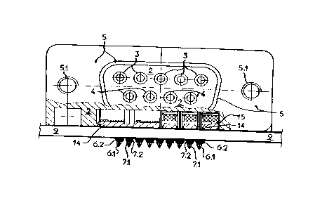
Figure 1 illustrates an angle-connecting device l, according to a preferred
embodiment of the
present invention, having been soldered onto a printed circuit board 9
(schematically
indicated, broken away). The angle-connecting device 1 as illustrated, is
positioned with its
basic body 2, surrounded by collar 5, onto the printed circuit board 9. The
soldering ends 6.1
and 7.1 of the signal lines, having an angle of approximately 90 °,
which pass through the
filter 10, are guided through perforations in the printed circuit board 9 to
the conductor tracks
provided therein, and are soldered to the latter via the soldering joints 6.2
and 7.2,
respectively.
The collar 5 surrounding the basic body 2 serves on the one hand for guiding
the connector
mating piece ( not shown in any more detail), which is connected to this angle
connecting
device and for the fastening of which screw connectors 5.1 are provided. On
the other hand,
the collar 5 establishes the connection of the ground connection, important
for trouble free
operation. For this purpose, the collar 5 is designed as a metallic body,
which is connected to
the general ground (not shown in any more detail) of the printed circuit board
9. The angle-
CA 02297686 2000-02-O1
connecting device designed in this way can be placed easily and un-
problematically onto a
printed circuit board and connected to the soldering joints provided for this
purpose of the
conductor tracks on this printed circuit board 9 via the soldering points 6.2
and 7.2,
respectively.
5
Figure 2 shows a cross section through such an angle-connecting device 1. The
basic body 2,
produced as a molding from plastic , receives the contact elements,
represented here as plug
in sockets 3 and 4, which are connected during plugging to the mating pieces
of the mating
contact to be connected,; these plug in sockets 3 and 4 are provided with
soldering pins 6 and
7. Such plug in sockets are produced , for example, by stamping from sheet
metal and rolling,
or by turning from suitable metal bars. The soldering pins 6 and 7, bent
around by 90°, form
the soldering ends 6.1 and 7.1 of the signal conductors, which are led-through
ducts 11,
provided in the filter plate 10, and are connected via soldering rings 11.1 to
the signal layers
of the capacitors (not shown here in any more detail), which are provided in
the filter plate 10
and the counter-electrodes of which are led out and connected to the general
ground.
The plate-shaped filter 10, for instance a planar filter known per se, lies in
a filter holder 12,
which receives it, holds it and shields it with its trough shaped design. For
this purpose, this
filter holder 12 is formed from metal sheet and is connected to the ground fo
the printed
circuit board (not shown in any more detail). Since the collar 5 is also
connected to this filter
holder 12, a continuous ground connection is endured without significant
inductances.
This filter holder 12 is provided outside the filter with an angled offset
12.1, which is chosen
such that the thickness corresponds to the plate of the filter 10, so that the
underside of the
plate of the filter 10 and the underside of the angled offset 12.1 are in
line. This angled offset
is filled with a plastic insert 13, which is inserted in said offset
essentially with a form fit. On
its underside facing the printed circuit board, the filter 10 is covered by a
centering plate 14.
This centering plate 14 is supported with its elevated , peripheral edge 15
against the
underside of this plate and is latched with the basic body 2 via latching
locations 16 on both
end faces. This centering plate 14 has the effect of interrupting a heat flow
occurnng during
the soldering on of the angle connecting device 1, the air filled cavity
formed by the elevated,
peripheral edge contributing in particular to this effect.
CA 02297686 2000-02-O1
6
Figure 3 shows in detail from Figure 2 an advantageous application of a filter
10, through
which soldering ends 6.1 and 7.1 bent away for connection to a printed circuit
board 9 are
led. Since, when pressure is applied to the soldering pins 6 and 7, extending
from the angle
connecting device 1, the bent away soldering ends 6.1 and 7.1 are moved, the
filter 10 is
S subjected to great mechanical stress at the locations of the soldering rings
11. To prevent
damage here, for instance tearing open of the soldering joints, a supporting
carrier 20 which
is provided with openings 21 in the same pattern of holes as the filter 10 is
inserted, facing
the bending location, so that the soldering ends 6.1 and 7.1 can be readily
led through the
filter 10 with the supporting carrier 20. The openings 21 in the supporting
carrier 20 enclose
the soldering ends 6.1 and 7.1 in such a way that during soldering the solder
flows through by
capillary action and plays a part in erecting the connection to the filter 10.
The soldering
pins or their soldering pin ends (6, 7; 6.1, 7.1) of the signal lines are
soldered in the region of
each of the soldering joints (22) such that the solder of each of the
soldering joints (22)
includes the respectively corresponding metallized terminal location (22.1) of
the planar
filter (10). This design has the advantage that the signal lines can be
initially installed in their
extended form; subsequent bending in desired directions no longer stresses the
planar filter;
shearing forces transmitted to the angle-connecting device 1 during insertion
also cannot
mechanically reach the filter 10 any longer. This embodiment is particularly
suitable in the
case of filters 10 which are extremely thin, and the substrate of which is
ground to size, since
the supporting plate can in this case bear with surface area contact.