Note : Les descriptions sont présentées dans la langue officielle dans laquelle elles ont été soumises.
.CA 02297716 2000-04-04
-1-
AUTOMATIC GAIN CONTROL CIRCUIT AND OPTICAL RECEIVER
Field of Invention
This invention relates to automatic gain control circuits. In particular, this
invention relates to an automatic gain control circuit particularly suitable
for processing the
output of an optical detector converting optical high-definition television
signals to electrical
signals for transmission to a receiver.
Background of the Invention
Optical fiber has become a popular medium for the transmission of
telecommunications sign;rls. The speed and accuracy of optical signals allows
for the
transmission of large voh.unes of information over a single optical fiber, and
with current
compression techniques the capacity of optical fiber transmission systems is
virtually
unlimited. Thus, optical fiber transmission systems are particularly useful
for high speed
transmissions involving large concentrations of data, such as high-definition
television
signals.
However, telecommunications equipment such as transmitters and receivers
still operate by processing; electrical signals. In a typical digital
television receiver, for
example, data is input to the receiver circuitry as a series of electrical
pulses. These pulses
represent pixel image data such as chrominance and luminance, synchronization
data such as
horizontal sync, vertical sync and frame sync, along with other
characteristics of the televised
image and associated data such as audio, closed captioning etc. The electrical
pulses occupy
standardized positions within a telecommunications signal, which are thus
decoded by the
receiver circuitry to creatf; an image on the television screen.
High-definition television (HDTV) has presented a considerable challenge to
conventional telecommunications technologies, due to the volume of information
required to
construct an HDTV image. Fiber optic telecommunications technology provides a
partial
solution, since the data rate of optical fiber transmissions easily
accommodates the 1.485
Gb/s data rate standard for HDTV transmissions. However, an opto-electric
coupler interface
is required which is capable of translating optical (typically laser-
generated) pulses received
.
CA 02297716 2000-04-04
-2-
from an optical fiber to corresponding electrical pulses which can be
processed by an HDTV
receiver.
One type of opto-electric coupler suitable for standard optically transmitted
telecommunications sign;~ls is a laser optical receiver, which emits a low
level electric pulse
corresponding to each optical pulse sensed by an optical detector. Existing
laser optical
receivers are capable of resolving optical pulses only to a power level of
approximately -15
dBm. However, SMPTE specification 292M for a laser optical receiver for HDTV
applications requires that the sensitivity of the receiver extend to at least -
20 dBm.
Conventional optical detectors tend to poorly process so-called "pathological"
signals, i.e. signals having; large numbers of consecutive zeros or ones,
because of the high
DC content and low frequency content resulting from the absence of zero-to-one
and one-to-
zero crossover points. Also, the output signal level from a conventional
optical detector tends
to fluctuate widely, while the DC restoration circuitry used to equalize the
signal output from
the optical receiver requires a relatively constant input signal in order to
perform properly.
Thus, conventional optical receivers are poorly suited for use in high-speed
applications such
as HDTV.
Summarrr of the Invention
The present invention overcomes these disadvantages by providing an optical
receiver having a sensitivity extending well below -20dBm, and an automatic
gain control
circuit therefor. The gain control circuit of the invention is self
stabilizing and provides a
consistently accurate and uniform output signal level to the DC restoration
circuitry, even
under pathological signal conditions.
The invention accomplishes this by coupling the low level signal produced by
an optical detector to a si~mal amplifier, the gain of which is controlled by
a negative
feedback circuit. The feedback circuit comprises a signal level detection
circuit coupled to
the amplifier output, in the preferred embodiment comprising high-speed
Schottky diodes
acting in conjunction with an operational amplifier. The Schottky diodes are
coupled to
ground through AC bypass capacitors, and oriented in opposite directions.
Thus, when the
amplified signal exceeds <~ conduction threshold of the Schottky diodes the AC
bypass
capacitors are respectively charged and drained, establishing a voltage
difference between the
CA 02297716 2000-04-04
-3-
input terminals of the operational amplifier. A current output from the
operational amplifier
to reduce the voltage difference is also fed to the gain control pin of the
signal amplifier,
reducing its gain.
The circuit of the invention thus establishes a negative feedback loop with
the
differential amplifier, to maintain a constant differential signal output
level. The differential
output signal is equalized. for transmission to switching, routing or
processing equipment or
to an HDTV receiver.
In the preferred embodiment the amplifier is a double-ended differential
amplifier, with the optical detector output fed into the high input and the
low input coupled to
ground, and the signal level detection circuit coupled in parallel to the
differential outputs.
Also, in the preferred embodiment the Schottky diode circuit clips peak levels
of the
differential output signal whenever they exceed a saturation voltage, which
further stabilizes
the differential output signal and avoids overloading of the DC restoration
circuitry.
The present invention thus provides an automatic gain control circuit,
comprising a differential ;amplifier having a high input adapted to receive a
high input signal,
a low input adapted to receive a low input signal, a high output for
outputting an amplified
high output signal, a low output for outputting an amplified low output signal
substantially
symmetrical with the high output signal, and a gain control input for
receiving a gain control
signal which controls the gain of the differential amplifier, and a feedback
circuit comprising
a signal level detection circuit comprising a first pair of diodes having
coupled anodes and
having cathodes respectively connected to the high output and low output, and
a second pair
of diodes having coupled cathodes and having anodes respectively connected to
the high
output and low output, and an operational amplifier having an inverting input
connected to
the coupled anodes of the first pair of diodes and to a first end of a first
capacitor, a non-
inverting input connected to the coupled cathodes of the second pair of diodes
and to a first
end of a second capacitor., the other ends of the first and second capacitors
being connected to
ground, and an output connected through a resistor to the inverting input and
connected to the
coupled anodes of the first pair of diodes, wherein an increase in the level
of the amplified
output signals causes a current to be withdrawn from the first capacitor which
lowers a
voltage at the inverting input and causes a current to be injected into the
second capacitor
which raises a voltage at the non-inverting input, causing a voltage
difference between the
CA 02297716 2000-04-04
-4-
output of the operational amplifier and the inverting input, whereby current
flowing from the
output of the operational amplif er to the inverting input flows to the gain
control input of the
differential amplifier to rc;duce the gain of the differential amplifier.
The present invention further provides an optical receiver for converting an
optical signal to an electrical signal, comprising an optical detector for
producing an electrical
input signal corresponding to an optical input signal detected by the optical
detector, a
differential amplifier having a high input adapted to receive the electrical
input signal, a low
input adapted to receive a low input signal, a high output for outputting an
amplified high
output signal, a low output for outputting an amplified low output signal
substantially
symmetrical with the high output signal, and a gain control input for
receiving a gain control
signal which controls the gain of the differential amplifier, and a feedback
circuit comprising
a signal level detection circuit comprising a first pair of diodes having
coupled anodes and
having cathodes respectively connected to the high output and low output, and
a second pair
of diodes having coupled cathodes and having anodes respectively connected to
the high
output and low output, and an operational amplifier having an inverting input
connected to
the coupled anodes of the first pair of diodes and to a first end of a first
capacitor, a non-
inverting input connected to the coupled cathodes of the second pair of diodes
and to a first
end of a second capacitor., the other ends of the first and second capacitors
being connected to
ground, and an output cormected through a resistor to the inverting input and
connected to the
coupled anodes of the first pair of diodes, wherein an increase in the level
of the amplified
output signals causes a current to be withdrawn from the first capacitor which
lowers a
voltage at the inverting input and causes a current to be injected into the
second capacitor
which raises a voltage at the non-inverting input, causing a voltage
difference between the
output of the operational amplifier and the inverting input, whereby current
flowing from the
output of the operational amplifier to the inverting input flows to the gain
control input of the
differential amplifier to reduce the gain of the differential amplifier.
The present invention further provides an automatic gain control circuit,
comprising an amplifier having an input adapted to receive an electrical input
signal, an
output for outputting an amplified output signal, and a gain control input for
receiving a gain
control signal which controls the gain of the amplifier, and a feedback
circuit comprising a
signal level detection circuit comprising a first pair of diodes having
coupled anodes and
having cathodes respectively connected to the output and to a reference
voltage, and a second
CA 02297716 2000-04-04
-5-
pair of diodes having coupled cathodes and having anodes respectively
connected to the
output and to the reference voltage, and an operational amplifier having an
inverting input
connected to the coupled anodes of the first pair of diodes and to a first end
of a first
capacitor, a non-inverting; input connected to the coupled cathodes of the
second pair of
diodes and to a first end of a second capacitor, the other ends of the first
and second
capacitors being connecte-d to ground, and an output connected through a
resistor to the
inverting input and connected to the coupled anodes of the first pair of
diodes, wherein an
increase in the level of th~~ amplified output signal causes a current to be
withdrawn from the
first capacitor which lowf;rs a voltage at the inverting input and causes a
current to be injected
into the second capacitor which raises a voltage at the non-inverting input,
causing a voltage
difference between the output of the operational amplifier and the inverting
input, whereby
current flowing from the ~~utput of the operational amplifier to the inverting
input flows to the
gain control input of the differential amplifier to reduce the gain of the
differential amplifier.
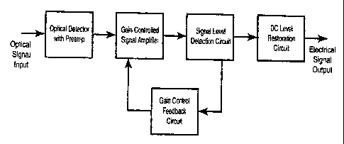
Brief Description of the I>rawin s
In drawings which illustrate by way of example only a preferred embodiment
of the invention,
Figure 1 is a block diagram illustrating an opto-electric coupler circuit of
the
invention,
Figure 2 is a schematic diagram of the opto-electric coupler circuit of Figure
l,
and
Figure 3 illustrates the waveforms of an HDTV signal through the stages of
the opto-electric coupler circuit of Figure 1.
Detailed Description of the Invention
Figures 1 and 2 illustrate a preferred embodiment of the invention for
converting
a laser optical signal recei~red through an optical fiber transmission system
to a digital electrical
signal adapted for processing by an HDTV receiver. T'he optical detector OD,
for example
FRM3Z231 by Fujitsu (Trademark), has an input optically coupled to an optical
fiber
transmission system (not shown) and a single-ended output for outputting an
electrical input
signal V;" corresponding to the optical input signal.
CA 02297716 2000-04-04
-6-
The optical detector OD output is coupled to the high input pin 1 of a
differential
amplifier U1 through two AC coupling capacitors C 16, C 17. Capacitors C 16, C
17 provide a
low RC time constant to stabilize pathological portions of the optical input
signal, i.e. segments
of the telecommunications signal having lengthy series of consecutive zeros or
ones, which tend
to have a large DC content and a low frequency content due to the absence of
zero-to-one and
one-to-zero crossovers and thus are subject to unusually high signal
degradation.
The differc;ntial amplifier U1, for example a Hewlett-Packard (Trademark) IVA-
05208 silicon bipolar 1.5 ~Ghz variable gain differential amplifier, has
differential input and
differential output capability. The low input pin 4 of the differential
amplifier Ul is coupled to
ground through capacitors C21, C22. A differential signal having a voltage
Vo"t proportional to
the voltage drop between V;" and ground is output as a differential signal
Vo"t represented by a
voltage difference between the high signal Vo"t+ output from pin 6 and the low
signal Vo"t-
output from pin 7. The gaiin of the differential amplifier U1 is controlled by
a feedback voltage
Vg~ at gain control pin 8,1>rovided by the feedback circuit FB described
below.
The high signal output pin 6 and the low signal output pin 7 of the
differential
amplifier U1 are coupled 1:o DC restoration circuit U2, for example a Gennum
(Trademark)
GS 1504 HDTV adaptive equalizer which serves as a serial digital receiver
interface, outputting a
digital HDTV signal along standard SOS2 cable to an HDTV signal receiver or
processor such as
a router, distribution amplifier, switcher or the like.
The high signal output pin 6 and the low signal output pin 7 are also
respectively
coupled to a feedback circuit FB through capacitors C9, C10 and C11, C12. In
the preferred
embodiment the feedback circuit FB comprises a signal level detection circuit,
connected in
parallel with the equalizer U2, and an operational amplifier U3. The signal
level detection circuit
preferably comprises high-speed dual common anode diode D1 and high-speed dual
common
cathode diode D2. The diodes D1, D2 may for example be commercially available
dual
Schottky (surface-barner) diodes, which are preferred for their high speed
operation and
sensitivity.
The common anodes of diode D1 are coupled to the inverting pin 3 of an
operational amplifier U3, and the common cathodes of diode D3 are coupled to
the non-
CA 02297716 2003-11-13
_7_
inverting pin t of the operational amplifier U3. The output from pin 4 of the
difaterential
amplifier tT3 is coupled through feedback circuit F13 to the gaita control pin
8 of differential
amplifier Ul, and through resistor R4 and capacitor G31 to the inverting input
pin 3 of op atop
U3. Input pin 3 of op amp U3 is coupled through resistor R3 to the damping
capacitor C27.
In operation, the optical detector UD outputs a low power signal Vi"
corresponding in frequency, and roughly proportional in amplitude, to optical
pulses received
from an optical fiber transmission system (not shown). The signal V~, has a
generally sinusoidal
waveform, due to the very low output level of the detector Ol~ (down to as low
as -23 d.t~m),
and can thus be considered as a low level analog input signal.
The signal V;" is filtered through capacitors C 16, C 17, which help to
stabilize
pathological portions of the signal V;", and input to high input pin 1 of
differential amplifier U 1.
The low input pin 4 oi'dii~erential amplifier Ul is biased to ground through
capacitors C2I,
C22, which in the circuit illustrated with V~~ _ +5 V and VSS = -5 V is held
at a slightly positive
voltage by voltage divider VD.
The differential amplifier U1 outputs a dil~erent~ial signal having a voltage
V~"~
proportionate to the voltage drop between Vi~ and ground, representing a
voltage difference
between a high signal Vo,~a. output from higli signal output pin 6 and a
mirror-image low signal
VQ,n output fr~~m low signal output pin ?_
The differential output signal V~"~ is AC coupled through a tapping circuit
comprising capacitors C9, C10 and C11, C12, and input to SDl+pin 4 and SDI-
pin 5 of
equaliser I12 tier DC restoration. The output of the equalizer U2 is coupled
to conventional SUfZ
coaxial cable which routes the equali~xd sigmal to HDTV equipment for fiurthcr
processing, or to
an HDTV receiver.
The gain of the differential amplifier U1 is controlled by a feedback voltage
Vx,;
at gain control pin 8, provided by the feedback circuit FB. When no liglxt
pulse is exciting
optical detector UD, the circuit is at a steady slntte. Tn this state there is
none or very little current
flowing through R3 and hence R4, th«s the output at pin 4 of operational
ampliticr U3 is
approximately at th,e same potential as pins 1 and 3 of its input. The voltage
divider VD sets up a
law DC bias (for example arcsund +2 V) at pin 1 of U3 and h~ce from output pin
4 of. the
CA 02297716 2000-04-04
_g_
operational amplifier U3 the gain control signal Vg~ is also low so the
differential amplifier U1 is
set to maximum gain. With no light pulse exciting the optical detector , the
differential input to
pins 4 and S of DC adaptive equalizer U2 is zero, and no signal is output from
the optical
receiver circuit.
When an optical pulse is detected by optical detector OD its output goes high
and
emits a signal V;", which is filtered through capacitors C 16, C 17 and fed to
input pin 1 of
differential amplifier Ul, which goes high. The voltage difference between
pins 1 and 4 of
differential amplifier U1 i;~ amplified and output from pins 6 and 7 of
differential amplifier U1
as symmetrical high and low signals Vo"t+ and Vo"t_, respectively, to produce
differential output
Slgnal Vouh
When the differential output signal Vo"t exceeds about 0.3 V (the conduction
threshold of the Schottky tiiodes), common cathode diode D2 injects current
into capacitor C28,
causing pin 1 of operational amplifier U3 to go high. Similarly, since Vo"t+
and Vo"t_ are
symmetrical, common anode diode D1 withdraws current from damping capacitor
C27 and pin
3 of operational amplifier U3 goes low. The output voltage Vg~ from pin 4 of
operational
amplifier U3 goes high to bring the voltage at inverting input pin 3 up to the
voltage at non-
inverting input pin 1. At the same time, the output voltage Vg~ is fed back to
gain control pin 8 of
differential amplifier Ul, reducing its gain.
The differential output signal Vo"t is thus fed to the input of the DC
restoration
circuitry at a consistent peak level, well within the ideal operating range of
the adaptive
equalizer U2. The automatic gain control circuit of the invention thus
provides the required
sensitivity and dynamic range to, and compensates for fluctuations in, the low
level output of the
optical detector OD.
The diodes D1, D2 thus serve a number of purposes. Primarily the diodes D1, D2
act as a charge pump, pushing current into capacitor C28 and drawing current
from capacitor
C27 whenever the differential output signal Vo"t rises, and thus act in
conjunction with the
operational amplifier U3 to create a negative feedback loop that controls the
gain of differential
amplifier U1. The diodes l~l, D2 clip the signal Vo"t when the level of
signals Vo"t+ and Vo"t_
exceed a saturation voltage, which helps to reduce the likelihood of
overloading adaptive
equalizer U2. Diodes D1, :D2 also provide some degree of loading due to the
intrinsic impedance
of the Schottky barner, which helps to eliminate reflections at the standard
HDTV frequency of
CA 02297716 2000-04-04
-9-
1.485 Gb/s. The diodes D 1, D2 provide rf detection and a convenient means for
termination to
the circuit board transmission line. Furthermore, their symmetrical
implementation provides
symmetrical clipping and loading on the signal propagating along the
transmission line.
Utilizing a differential amplifier U1 with differential input and differential
output
provides the advantage that the amplified output signal from the differential
amplifier Ul is
doubled in amplitude, which allows for greater control of the feedback voltage
Vg~. This
configuration also allows ~Por better termination to the transmission line.
However, a single-
ended version of the automatic gain control circuit and optical receiver
should also be effective,
with one end of each diode D 1, D2 connected to the amplified output and the
other ends of the
diodes coupled to a steady DC reference voltage.
A preferred embodiment of the invention having been thus described by way
of example only, it will bE: apparent to those skilled in the art that certain
modifications and
adaptations may be made without departing from the scope of the invention. The
invention
includes all such embodiments as fall within the scope of the appended claims.