Note : Les descriptions sont présentées dans la langue officielle dans laquelle elles ont été soumises.
CA 02298456 2000-02-16
TITLE OF THE INVENTION
Optical Recording Medium
BACKGROUND OF THE INVENTION
Field of the Invention
This invention relates to a phase change optical recording medium. More
particularly, it relates to a phase change optical recording medium capable of
high-
speed direct overwriting.
Description of the Prior Art
As a practical example of an overwritable optical disc, employing a phase
change recording material, a so-called DVD-RAM is commercialized, in which a
linear
velocity of 6 m/sec, a bit length of 0.41 /,cm, track pitch of 0.74 pm, a
laser wavelength
of approximately 650 nm, a data transfer rate of 11 Mbpa and a recording
capacity of
2.6 GB have been realized.
For realizing a larger capacity and a higher transfer rate, it is effective to
reduce
the spot size of the recording laser and to raise the recording linear
velocity. As a
practical technique for reducing the spot size of the recording laser light,
there are a
method of shortening the laser wavelength and a method of increasing the
numerical
aperture of the objective lens.
In particular, if the method of reducing the laser wavelength and the method
of '
increasing the numerical aperture of the objective lens are used in
combination, the
spot size may be made smaller than if one or the other method by itself is
used. For
1
CA 02298456 2000-02-16
example, if a blue to purple laser having a wavelength in the vicinity of 400
nm is used
as a light source and an objective lens with a numerical aperture NA of 0.85
is used,
it is theoretically possible to realize a still higher recording density.
However, the condition for performing direct overwrite at an elevated speed on
the phase change optical disc is more stringent for the following reason:
In general, in a phase change optical disc, the laser light of a high power is
illuminated thereon to fuse the recording layer by raising its temperature to
higher than
the fusing temperature of the recording layer. The recording layer then is
quenched
to write recording marks. The recorded marks are crystallized, that is erased,
by being
maintained in a temperature range intermediate between the crystallization
initiating
temperature and the melting point of the recording layer for a time necessary
for the
recording layer to become crystalline.
If the method for shortening the laser wavelength or the method of increasing
the numerical aperture of the objective lens is adopted, and/or under the
conditions of
a higher recording linear velocity, the temperature on. a point.on the optical
disc is
changed within a shorter time than conventionally. Fig.24 shows, as an example
showing the results of how the temperature on a given point on the disc is
varied- with
lapse of time. As may be seen from Fig.24, the time during which the
temperature is
kept higher than the crystallization temperature, assumed to be 400 C as an
example,
becomes shorter the shorter is the recording and/or reproducing wavelength.
Thus, in a recording material having the crystallization speed which is the
same
2
CA 02298456 2000-02-16
. , , .
as the conventional speed, it becomes difficult to crystallize, that is to
erase, the
recorded amorphous marks.
If, in case of a direct overwrite (DOW) in which recording is made as the sole
laser light power level is controlled temporally, the spot size is small, or
the recording
linear speed is high, the result is promoted distortion of the mark shape
ascribable to
the difference in the physical properties between the amorphous phase and the
crystalline phase, as characteristic of the phase-change recording. That is,
under this
condition, if a mark is overwritten in superposition on already written
recording marks,
the recording marks tend to be larger in size than if the marks are newly
written in a
blank crystalline state area.
This is caused.by the difference in the response to the laser light (optical
constant), the manner of heat transmission caused by the reaction with the
laser light
(thermal conductivity) or in the manner of use of the heat between the
amorphous
phase and the crystalline phase. It is noted that latent heat at the time of
fusion is
unnecessary. Meanwhile, if the spot size is large,.with the linear. speed
being low,
temporary temperature changes of the recording film are moderate, such that
heat is
conducted before the already present marks reach the laser so that the
crystallization
temperature is kept from the outset. Therefore, the state equivalent to a
state in.which
the marks in actuality were not present (preceding crystallization) is
realized, thus
evading the aforementioned problem.
Due to this problem, a higher recording density and a higher transfer rate are
3
CA 02298456 2000-02-16
difficult to achieve in case of a routinely used phase change optical disc
having a four-
layer structure comprised of a ZnS-Si02 layer, a recording layer, a ZnS-Si02
layer and
a reflective layer with the Ac/Aa ratio being lower than 0.9, Ac being a rate
of
absorption for the recording layer in the crystalline state and Aa being a
rate of
absorption for the recording layer in the amorphous state. For example, it has
been
shown experimentally that, as the linear speed is higher, the j itter value
become worse,
as shown for example in Fig.25.
For solving this difficulty, it may be envisaged to increase the
crystallization
temperature of the recording layer. That is, it suffices if the time necessary
for
crystallization is shortened to raise the rate of erasure to render preceding
crystallization liable to occur more readily.
However, it is virtually impossible to find a material in which phase change
may
occur reversibly and which has a crystallization temperature not lower than
that
realized in the past and to apply this material to an optical disc.
With this in view, there is proposed in Japanese Laying-Open Patent H-1-92937,
Japanese Laying-Open Patent H-6-195747 or in Japanese Laying-Open Patent H-9-
532424 a technique in which the crystallization promoting material, effective
in
improving the crystallization speed of the amorphous phase is provided
adjacent to the
recording layer in place of raising the crystallization speed of the recording
material
itself, in order to increase the crystallization speed of the recording layer.
This technique has, however, a drawback that it tends to lower the storage
stability of
4
CA 02298456 2000-02-16
the recording marks in a temperature range encountered under the routine using
conditions and that the recording marks are erased by the laser light used for
reproduction.
On the other hand, there is also proposed in, for example, Japanese Laying-
Open Patent H-8-124218 or Japanese Laying-Open Patent H-9-91755 a technique in
which the state of the. rate of absorption usually higher in the amorphous
phase than
in the crystallization phase is reversed by controlling the layering structure
of the
optical thin film, that is in which the temperature rising rate of the
crystalline portion
and that of the amorphous portion are balanced relative to each other to
correct the
distortion of the mark shape, that is the technique of controlling the rate of
absorption
to correct the distortion of the mark shape.
This technique has, however, a drawback that the degree of freedom in optical
designing, such as rate of absorption or reflectance, is lowered, and that the
durability
against repeated overwriting is not that high.
Moreover, in the short wavelength conditions, the time during which the
temperature higher than the crystallization temperature is maintained becomes
shorter,
with the result that the basic erasure capability, such as erasure ratio by
the dc light,
which is an indispensable condition for producing the effect of controlling
the rate of
absorption, falls short.
SIJMMARY OF TBE INVENTION
It is therefore an object of the present invention to provide an optical
recording
CA 02298456 2000-02-16
medium which is able to cope with high recording density and a high transfer
rate
corresponding to the shortened wavelength and which is able to realize optimum
direct
overwrite without lowering the repetitive durability or storage stability of
recorded
signals.
The present invention provides an optical recording medium including a
recording layer formed at least of a phase change material, with the
wavelength of the
recording and/or reproducing laser light being 380 to 420 nm, wherein a ratio
Ac/Aa,
where Ac is the absorption rate of said recording layer in a crystalline state
and Aa is
the absorption rate of said recording layer in an amorphous state, is not less
than 0.9,
and wherein a crystallization promoting layer promoting the crystallization of
said
phase change material is contacted with at least one surface of said recording
layer.
The basic concept of the present invention is to use absorption rate control
and
crystallization promotion in combination. By such combination, it is possible
to
positively compensate the difference between the physical properties of the
crystal
phase and those of the amorphous phase to realize optimum direct overwrite.
The individual techniques, that is the absorption rate control and
crystallization
promotion, can be suppressed so that these problems are not apparent, such
that
repetitive durability or storage stability of the recorded signals is not
impaired.
The absorption rate control and crystallization promotion represent techniques
contradictory for the layer of the phase change material, such that, if these
are
combined together, it may be feared that the merits of the two techniques
cancel each
6
CA 02298456 2000-02-16
other. For this reason, attempts in combining these two techniques have
scarcely been
made in the prior art.
The present inventors have found that a problem arises that absorption rate
control fails to lead to the lowered jitter value even with absorption rate
control such
that some measured need to be taken to combat this problem.
The present inventors have investigated into the combination of the absorption
rate control and. crystallization promotion and have arrived at the
information that the
shortcomings ofthe respective techniques are hardly manifested subjectto
appropriate
designing.
That is, the absorption rate control lowers the absorption of the recording
film
by a layered film structure, as a result of which the erasure sensitivity is
lowered, even
if the recording medium is superior in repetitive reproduction and durability.
Conversely, if high-speed crystallization is enabled by the provision of the
crystallization promoting layer, the repetitive reproduction and durability
are not
optimum, even if erasure sensitivity is improved.
If the two techniques are combined together, recording marks are erased when
desired, thus enabling high-speed overwrite. On the contrary, the recording
marks are
not erased when it is not desired to erase the marks. For example, the cross-
write
characteristics are improved to optimize the storage stability, while the rise
in the j itter
value accompanying the increased number of times of playback is only small.
7
CA 02298456 2000-02-16
This finding has not been premeditated in the past, and has been first reached
by the present iriventors.
According to the present invention, high speed or high transfer rate and large
capacity, as two major factors required in achieving high performance of the
optical
disc, may be realized, whilst the high reliability, which is in a relation of
trade-off with
respect to the high speed of the optical disc, can be achieved simultaneously.
That is, the present invention provides a technique of realizing the high
performance and high reliability in a well-balanced manner and hence a
technology
which is indispensable for laser wavelength shortening, multi-layering of the
optical
disc, realization of a finer spot size or near-field recording with a phase
change
recording.medium.
BRIEF DESCRIPTION OF THE DRAWINGS
Fig. 1 is a schematic cross-sectional view showing essential portions of a
basic
illustrative structure of an optical disc embodying the present invention.
Fig.2 is a diagrammatic view for defining thereflectance, transmittance and
the
absorption rate in a multi-layer film.
Fig.3 is a graph showing temperature dependency of the nucleation speed and
the crystal growth speed.
Fig.4 is a schematic cross-sectional view showing an illustrative structure of
an
optical disc having a reflective layer.
Fig.5 is a schematic cross-sectional view showing an illustrative structure of
an
8
CA 02298456 2000-02-16
optical disc having a light transmission protective layer.
Fig.6 is a schematic cross-sectional view showing an illustrative structure of
an
optical disc having multi-layered reflective and recording layers.
Fig.7 is a schematic cross-sectional view showing an illustrative structure of
an
optical disc having dielectric layers between neighboring layers.
Fig.8 is a a schematic cross-sectional view showing an illustrative structure
of
an optical disc having a light absorption control layer.
Fig.9 is a graph showing changes in optical constants of the recording layers
with the recording and/or reproducing wavelengths.
Fig. 10 is a diagrammatic view showing an illustrative optical disc employing
a
transmission type reflective layer.
Fig. 11 is a graph showing changes in Ac, Aa, Rc and Ra of a recording layer
at
a wavelength of 640 nm.
Fig.12 is a graph showing changes in Ac, Aa, Rc and Ra of a recording layer at
a wavelength of 407 nm.
Fig. 13 is a diagrammatic view of an optical disc of Example 1.
Fig.14 is a graph showing changes in Ac, Aa, Rc and Ra of a recording layer at
a wavelength of 407 nm.
Fig.15 is a graph showing changes in Ac?Aa at a wavelength of 407 nm.
Fig.16 is a graph showing changes in the jitter value with the number of times
of direct overwrite operations.
9
CA 02298456 2000-02-16
Fig.17 is a schematic cross-sectional view showing an illustrative structure
of
an optical disc manufactured according to an alternative embodiment.
Fig. 18 is a schematic cross-sectional view showing a structure of an optical
disc
manufactured according to another alternative embodiment.
Fig. 19 is a schematic cross-sectional view showing a structure of an optical
disc
manufactured according to still another alternative embodiment.
Fig.20 is a schematic cross-sectional view showing a structure of an optical
disc
manufactured according to still another alternative embodiment.
Fig.21 is a schematic cross-sectional view showing a structure of an optical
disc
manufactured according to still another alternative embodiment.
Fig.22 is a schematic cross-sectional view showing a structure of an optical
disc
manufactured according to yet another alternative embodiment.
Fig.23 is a graph showing changes in the jitter value with the number of times
of overwriting in case of using a GaN based semiconductor laser.
Fig.24 is a graph showing difference in the crystallization temperature
holding
time with the difference in the linear speed, numerical aperture NA and the
wavelength.
Fig.25 is a graph showing the relation between the linear velocity and the
jitter
in a conventional phase change optical disc.
DESCRIPTION OF THE PREFERRED EMBODIMENTS
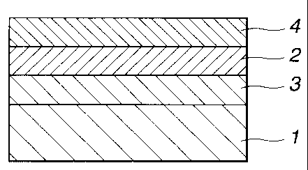
Referring to the drawings, an optical recording medium (optical disc)
according
CA 02298456 2000-02-16
to the present invention will be explained in detail.
Fig.1 shows a basic structure of an optical disc embodying the present
invention. On a transparent substrate 1, with a thickness not less than 0.3
mm, there
is formed a recording layer 2. In contact with both surfaces of the recording
layer 2
are formed crystallization promoting layers 3, 4.
Only one crystallization promoting layer may be formed on one or the other
surface of the recording layer 2.
In a phase change optical recording medium, the ratio Ac/Aa, where Ac is the
absorption rate of a recording layer 2 when the recording layer is in the
crystalline
state and Aa is the absorption rate of a recording layer 2 when the recording
layer is
in the amorphous state, is routinely on the order of 0.8.
According to the present invention, the ratio Ac/Aa, where Ac is the
absorption
rate of a recording layer 2 when the recording layer is in the crystalline
state and Aa
is the absorption rate of a recording layer 2 when the recording layer is in
the
amorphous state, is set, by proper film designing, to not less than 0.9, for
the
wavelength of the recording and/or reproducing laser light, hereinafter the
same. In
particular, the absorption rate Aa when the recording layer is in the
amorphous state
is preferably not less than 60%.
By setting the absorption rate ratio Ac/Aa to not less than 0.9, the
crystalline
portion tends to be heated more easily, relatively, such that the size of the
recording
mark written in a portion of the blank crystalline state can be made to
approach to the
11
CA 02298456 2000-02-16
size of the recording mark overwritten on the recording mark in the amorphous
state.
However, if the ratio Ac/Aa is increased excessively, the possibility is high
that
the direction in which the ratio is increased affects the reflectivity
designing or thermal
designing to deteriorate the comprehensive balance of the optical recording
medium.
This naturally sets a range of allowance, that is an upper limit, of the
aforementioned absorption rate ratio. However, this range of allowance also
differs
with the wavelength of the recording and/or reproducing light, such that, with
the
wavelength ranging between 380 nm and 420 nm, the absorption rate ratio is
preferably set to not larger than 2.5.
Meanwhile, the absorption rate ratio Ac for the crystalline state of the
recording
layer is the absorption rate ratio in the recording layer in the crystalline
state with
respect to the wavelength of the recording and/or reproducing laser light.
Similarly,
the absorption rate ratio Aa for the amorphous state of the recording layer is
the
absorption rate ratio in the recording layer in the amorphous state.
These values cannot be measured directly in a multi-layered structure. It is
necessary to calculate the intensity of lighjt absorbed in the recording layer
as resut of
multi-path interference by the multiple layers and to divide the cal;culated
light
intensity with the incident light intensity.
Thus, according to the present invention, the absorption rates Ac, Aa as
follows:
In the case of the multi-layer film (m layer) shown in Fig.2, the reflectance
R
the transmittance T and the absorption rate ratio of the disc, the absorption
rate ratio
12
CA 02298456 2000-02-16
A12 in the I2 layer, such as a recording layer and the absorption rate ratio
A,,n-, in the
Im-1 layer, such as the recording layer, are defined as follows:
reflectance R of the disc: 100xIr/I (%)
transmittance T of the disc: 100xIt/I (%)
absorption rate ratio A of the disc: 100X(I - Ir - It)/I (%)
absorption rate A12 in the 12 layer (e.g., recording layer): 100 X I2/I (%)
absorption rate Alm-, in the I,m-, layer (e.g., reflecting layer): 100 x
I,m_1/I (5)
it being assumed that the light incidence occurs only in the perpendicular
direction, with the oblique incident component being disregarded, and that the
respective interfaces are planar, with the effect of micro-irregularities of
the groove
etc being disregarded, and that only multi-path interference on the multi-
layer film
being taken into account, with the reference incident light intensity I being
the actual
incidfent light intensity Ix less the intensity of the reflected light Iy on
the surface.
In the above definition, Ir is the intensity of the reflected light from the
multi-
layer film, It is the intensity of light transmitted through the multi-layer
film, I12 is the
intensity of light absorbed by the 12 layer, such as the recording layer and
Iim-, is the
intensity of light absorbed by the Im-, layer, such as a reflective layer.
The absorption rate ratio Ac or Aa is the intensity of light absorbed by the
recording layer in the crystalline or amorphous state as a result of multi-
path
interference divided by the intensity of the incident light I to the multiple
films.
The above calculations of the multi-path interference are possible by
13
CA 02298456 2000-02-16
introducing the characteristic matrix if the laser light wavelength, film
thicknesses of
the respective layers and complex refractive index (n -1k) are known.
There are a number of publications issued concerning the methods for
calculating the multi-path interference, such as, for example, Tatsuo Tsuruta,
"Applied
Optics I" (1-2-2: Light Intensity), "Applied Optics II" (4-3-2: Multi-Layer
Film)
issued by Baifukan Publishing Company Ltd., and Shiro Fujiwara (editor),
Optical
Technical Series II "Optical Thin Film" (Capter 3, Multi-layer Film and four-
Terminal
Circuit), issued by Kyoritsu Publishing Company Ltd.
As may be seen from these publications, the relation between the tangential
component of the electrical and magnetic fields on the Jth boundary and those
on the
(J-1)st boundary can be known.
The light energy I can be represented by an average value < S I > of the
absolute
values of the pointing vector S, whilst the absorption AJ and the absorption
rate ratio
of the J'th layer can be represented by A, = I,_, - I, and by (IJ-, - I,)/Io;
where Io is the
incident light energy after subtraction of surface reflection), respectively.
The algorithm for these calculations are well-known, such that these
calculatins
can be made by emnploying the algorithms. The expression "only so-and-so in a
monolayer" means the case for m = 1.
The operation of the crystallization promoting layers 3, 4 is hereinafter
explained.
In general, the crystallization of the amorphous phase proceeds in two stages,
14
CA 02298456 2000-02-16
namely in the nucleation stage and in the crystal growth stage. If assumed
that the
generation of crystal nuclei occurs at random in all sites in the interior of
the
amorphous phase, the nucleation speed is increased with rise in temperature to
reach
the maximum value at a temperature slightly above the glass transition
temperature Tg,
with the nucleation speed rapidly decreasing at temperatures higher than the
temperature slightly above the glass transition temperature. On the other
hand, the
growth speed U becomes maximum at a temperature close to the melting point Tm.
In the case of the amorphous mark of the optical disc, in which the layer of
the
recording material 3 has two surfaces, in contradistinction to the above-
mentioned
supposition, nucleation is likely to take place on the boundary surfaces
between a layer
of the recording material 3 and layers on its both sides. In this case, the
chemical or
physical properties of the boundary surfaces are known to affect the frequency
of the
nucleation appreciably.
Thus, according to the present invention, the crystallization promoting layers
3, 4 are-provided adjacent to the recording layer 2 to control the generation
frequency
of the crystal nuclei. It is noted that only one of the layers 3, 4 suffices.
That is, by
providing the crystallization promoting layers 3, 4 adjacent to the recording
layer 2,
it is possible to promote the growth of crystal nuclei to raise the speed of
crystallization. This leads to a sufficient overwrite erasure ratio, even
under high
transfer rate condition, thus assuring satisfactory jitter values.
It is noted that the crystallization promoting layers 3, 4 may be the same
layer
CA 02298456 2000-02-16
operating simultaneously as the dielectric layers. For example, ZnS-Si02, in
particular
having a molar ratio of approximately 4:1, may be used as an ordinary
dielectric layer,
or the dielectric material itself may be formed of a crystallization promoting
material.
That is, if the crystallization promoting layer formed of a crystallization
promoting
material, enumerated below, is provided adjacent to the recording layer 2, it
does not
matter whether or not there is provided the dielectric layer or what sort of
the material
is used for the dielectric layer. It has also been known that, if the
crystallization
promoting layer is provided adjacent to at least one of the surfaces of the
recording
layer 2, the nucleation speed of the recording layer 2 is higher than if there
lacks the
crystallization promoting layer. It is however noted that the crystallization
promoting
effect achieved is higher if the crystallization promoting layers are provided
adjacent
to both surfaces of the recording layer 2.
As the materials capable of promoting the crystallization, it has been known
thatt the materials used hitherto as a dielectric material in the optical
recording
medium, excluding sulfides, and having the value ofthe extinction coeff'icient
k for the
wavelength of the recording and/or reproducing laser of 0.3 or less, may be
used
satisfactorily. The crystallization promoting layer may be formed exclusiveluy
or
mainly of nitrides, oxides, carbides, fluorides, nitro-oxides, nitro-carbides
or oxo-
carbides of metal or metalloids, such as Al, Si, Ta, Ti, Zr, Nb, Mg, B, Zn,
Pb, Ca, La
or Ge. Specifically, layers constituted exclusively or mainly by AINx, where
0.5 s x
s 1, in particular AIN, A12O3-x, where 0 s x s 1, in particular A1203,
Si3N4_X, where 0
16
CA 02298456 2000-02-16
s x s l,in particular Si3N4, SiO,, where 1 s x s 2, in particular Si02, SiO,
MgO, Y203,
MgA1204, TiOX, where 1 s x s 2, in particular Ti02, BaTiO;1 StTiO3, TazO5-,,
where
0 s x s l,in particular Ta2O5, GaO, where 1 s x s 2, SiC, Ga-N, Ga-N-O, Si-N-
O,
CaF2, LaF, MgF2, NaF, ThF4, exhibit the function of promoting the
crystallization.
Also, layers formed of a miuxture of the above materials, for example, a layer
formed
of A1N-SiO21 similarly exhibits the function of promoting the crystallization.
However, these materials cannot be said to be sufficient in crystallization
promoting functions, such that optimum signal characteristics cannot be
achieved
under severe conditions.
Thus, of the materials havingthe function of promoting the crystallization,
one
ormore of Si-C, Si-C-O,.Si-C-H, Si-C-H-O, Si-N, Si-N-O, Si-N-H, Si-N-H-O; Si-C-
N,
Si-C-N-O, Si-C-N-H, Si-N-H-O, Si-O, Si-O-H, Al-N and Al-O, in particular, is
preferably used as the crystallization promoting layer.
Examples of the materilas include Si-C, Si3N41 Si02, A1N, A1203 and materials
mainly composed of these compounds and containing oxygen, hydrogen or
nitrogen.
It has been confirmed that these materials exhibit outstanding crystallization
promoting effect, in combination with absorption rate ratio control (Ac/Aa z
0.9),
characteristic of the present invention, to give a large jitter value
diminishing effect
and improved repeated overwrite durability, as demonstrated in the Examples of
the
invention. In the configuration shown in an illustrative Examole, such a
material
composed mainly of SiC and into which 0 or H was introduced was superior.
17
CA 02298456 2000-02-16
Moreover, optimum characteristics were achieved in cross-write or mark
preservation
stability. On the other hand, the above materials were superior as a material
contacting
with the recording layer in that these materials were not susceptible to
peeling or
alloying on an interface with the recording layer and exhibited only low light
absorption capability. The above accounts for the preferability of the above-
mentioned crystallization promoting materials.
Although the film thickness of the crystallization promoting layer is not
prescribed specifically, the film thickness of not less than I nm is desirable
for forming
a homogeneous film. For the configuration shown by the illiustrative example,
the film
thickness not less than 2 nm demonstrated a jitter value diminishing effect.
Although there is no limitation to the manufacturing method for the
crystallization promoting layer, several examples are. given below:
First, SiC can be formed by a SiC target by an RF sputtering method, using an
Ar gas.
. Si3N4 can be formed by film forming by a reactive sputtering an Si target
using
an N2 gas
Si02 can be formed by film deposition by RF sputtering a Si02 target using ab
Ar gas.
AIN can be formed by reactive sputtering an Al target using an ArN2 gas.
A1203 can be formed by reactive sputtering an Al target using e.g., an Al
target.
Si-C-H-O can be formed by film forming by RF sputtering a SiC target using
18
CA 02298456 2000-02-16
an Ar gas containing H20 in an amount of e.g., 300 ppm.
By providing the crystallization promoting layers 3, 4, generation of crystal
nuclei is promoted to raise the crystallization speed. This is extremely
advantageous
in direct overwriting.
However, if the cross-sectional speed is excessively high, the recording
marked
formed (amorphous marks) tend to be impaired in preservation stability.
Conversely,
if the crystallization speed is excessively low, the effect proper to the
crystallization
promoting layers 3, 4 cannot be expected to be displayed. In this
consideratin, the
crystallization speed needs to be controlled to a moderate value.
The above is the basic configuration of the optical disc embodying the present
invention. The layer structure can, however, be modified in desired manner.
Fig.4 shows an example of forming the reflecting layer 5. In this case, the
reflecting layer 5 and the recording layer are formed in this order on the
substrate 1.
Thus, the recording and/or reproducing laser is illuminated from the side of
the
recording layer 2 for recording and/or reproduction. In this case, a light
transmission
protective layer 6 is preferably formed on the recording layer 2.
Fig.5 shows an example of forming the light transmission protective layer. In
the present example, the reflecting layer 5, recording layer 2 and the light
transmission
protective layer 6 are sequentially formed and crystallization promoting
layers are
formed adjacent to both sides of the recording layer 2.
Thus, in the present optical disc, the recording and/or reproducing light is
19
CA 02298456 2000-02-16
illuminated from the side of the light transmission protective layer 6 for
recording
and/or reproduction for the recording layer 2.
The configuration of the optical disc is not limited to the above-described
configurations. For example, the recording layer 2 and the reflecting layer 5
may be
formed in this order on the transparent substrate 1 so that recording and/or
reproduction will be performed from the side of the transparent substrate 1.
However,
if the recording and/or reproduction is performed from the side of the light
transmission protection layer 6, the numerical aperture of the objective lens
can be
increased to achieve a high recording density as the skew margin is
maintained, thus
achieving an outstanding effect proper to the present invention. The reason is
that, by
reducing the size of the recording spot, the temperature on a given spot of
the optical
disc is changed in a short time so that direct overwriting is rendered more
difficult in
the same manner as when the linear speed is increased.
Alternatively, the recording layer may be constituted by a first recording
layer
2A and a second recording layer 2B, as shown in Fig.6. Moreover, the
reflectirig layer
may be a double-layer film constituted by a first reflecting layer 5A and a
second
reflecting layer 5B. By constituting the reflecting layer in a multi-layer
structure, such
as double-layer structure, the degree of freedom in optical designing is
increased. If
the reflecting layer is constituted by two or more layers, different as to the
material,
composition or complex refractive index, a dielectric layer(s) may be inserted
at
optional positions between the reflecting layers. The number of layers of the
dielectric
CA 02298456 2000-02-16
layers inserted is also optional.
In addition, dielectric layers 7 may be arranged between the light
transmission
protective layer 6 and the recording layer 2, between the recording layer 2
and the
reflecting layer 5 and between the reflecting layer 5 and the transparent
substrate 1.
The dielectric layers are arranged in this manner at least at one site. Fig.7
shows an
illustrative structure in which the dielectric layers 7 (7C, 7B, 7A) are
arranged at all
of the three sites.
By arranging these dielectric layers 7 and adjusting their film thicknesses,
it
becomes possible to control the optical properties to control the above-
mentioned
absorption rate ratio.
The respective dielectric layers 7 may each be formed as a multi-layered film,
e.g., a two-layered film. It is also possible to provide a light absorption
controlling
layer 8 at a site closer to the recording and/or reproducing light
illuminating side than
the recording layer 2, to control the absorption rate ratio, as shown in
Fig.8. It is
similarly possible in this case to arrange the dielectric layers 7 (7D, 7C,
7B, 7A) at
optional sites inclusive of the site between the light absorption controlling
layer 8 and
the light transmission protective layer 6 or the site between the light
absorption
controlling layer 8 and the recording layer 2.
The light absorption controlling layer 8 may similarly be constituted by two
or
more layers different as to the material type, composition or complex
refractive index.
In such case, a dielectric layer(s) may be inserted at optional positions
between the
21
CA 02298456 2000-02-16
reflecting layers. The number of layers of the dielectric layers inserted is
also optional.
Of the above-mentioned configurations, the preferred configuration is such a
one comprised of a reflecting layer, a first dielectric layer, a first
crystallization
promoting layer, a recording layer, a second crystallization promoting layer,
a second
dilectric layer and a light transmission protective layer, arranged
sequentially on a
substrate.
It is preferred in this case to set the thicknesses of the substrate,
reflecting layer,
first dielectric layer, first crystallization promoting layer, recording
layer, second
crystallization promoting layer, second dielectric layer and the light
transmission
protective layer to 1.0 to 1.2 mm, 5 to 200 nm, 5 to 70 nm, 1 to 20 nm, 5 to
25 nm, 1
to 20 nm and to-0.5 to 0.15 nm, with the second dielectric layer being a momo-
layer
or multi-layer film at least including a dielectric layer with a thickness of
5 to 100 nm.
In the optical disc of the above structure, the material used for the
transparent
substrate is preferably plastics materials, such as polycarbonate or acrylic
resin, in
view of cost. However, glass may also be used. For fabrication, an injection
molding
method, or a photopolymer (2P) method, employing a LTV light curable resin,
may be
used. However, any other suitable method, which possibly gives a desired disc
shape,
e.g., a disc shape with a thickness of 1.1 mm and a diameter of 120 mm, and
optically
sufficient substrate surface smoothness, may be used.
Although there is no particular limitation to the substrate thickness, the
thickness not less than 0.3 mm and not larger than 1.3 mm is particularly
preferred.
22
CA 02298456 2000-02-16
If the substrate thickness is smaller than 0.3 mm, disc strength tends to be
lowered.
Conversely, if the substrate thickness is thicker than 1.3 mm, the disc
thickness is
thicker than 1.2 mm of the CD or DVD, such that there is a possibility that
the same
disc tray cannot be used in commercializing a driving device adapted to cope
with all
of these discs.
Ifthe laser light for recording and/or reproduction falls on the light
transmission
protective layer, the substrate material may be an opaque material, such as
metal.
Conversely, if the laser light falls on the substrate, such a material that
scarcely
exhibits absorption capability for the wavelength of the recording and/or
reproducing
laser light (380 to 420 nm) is used. At any rate, the substrate type may be
optional.
Meanwhile, if the recording and/or reproducing light falls on the substrate,
the
forming sequence of the layers provided betweenthe substrate and the light
transmission protective layer is reversed from that when the recording and/or
reproducing light falls on the light transmission protective layer.
The surface of the optical disc provided witht the multi-layer recording. film
may be formed with inundated grooved tracks. The light beam is can be moved to
an
optional site on the disc with the groove as guide. The groove shape may be
spiral or
concentric or may be in the form of a pit string.
The light transmission protective layer is preferably formed of a material not
having the absorption capability with respect to the wavelength ofthe
recording and/or
reproducing laser (380 nm to 420 nm). Specifically, the light transmission
protective
23
CA 02298456 2000-02-16
layer is formed of a material having a transmittance not less than 80%. The
thickness
of the light transmission protective layer is preferably not larger than 0.3
mm. In
particular, a hitherto unprecedented high recording density can be achieved by
combining the thickness ranging between 3 and 177 m with a high numerical
aperture
NA, such as 0.85.
For preventing dust deposition or scratching on the surface of the light
transmission protective layer, a protective layer formed of an organic or
inorganic
material may be formed, which preferably has only negligible absorption
capability
with respect to the wavelength of the recording and/or reproducing laser
light.
The method for fabricating an optical disc for performing recording and/or
reproduction from the side of the light transmission protective layer may
roughly be
classified into the following two methods:
The first method layers a multi-layered film on a substrate formed with a
guide
groove and ultimately forms a smooth light transmission protective layer. The
second
method, on the other hand, layers a muti-layered film on a light transmission
protective
layer formed with a guide groove, and ultimately forms a smooth substrate.
Since the process step of forming inundsations on the light transmission
protective layer or the process step of forming a multi-layered film is not
necessarily
easy, the first method is more preferred in view of mass-producibility.
If the first method is used, such a method may be used in which an optically
sufficiently smooth sheet (film), 0.3 mm in thickness, formed of a plastics
material,
24
CA 02298456 2000-02-16
such as polycarbonate or acrylic resin, is stuck on UV light irradiation,
using a UV
light curable resin as an adhesive. Such a method may be used in which a UV
light
curable resin is applied to a desired thickness not larger than 0.3 mm, by
e.g., a spin
coater, followed by UV light irradiation.
The light transmission protective layer may be of any suitable configuration
or
may be formed by any suitable method provided that it has the transmittance
not less
than 90% and a thickness not larger than 0.3 mm. The light transmission
protective
layer may also be formed with an inundated grooved track(s). The inundated
grooved
track(s) may also be formed in the light transmission protective layer by
e.g., an
injection molding method, a photopolymer (2P) method, or a method of
transcribing
inundations by pressure bonding or pressurization.
In the optical disc of each of the above configurations, the recording layer 2
is
formed of a phase change material, that is, a material which undergoes
reversible
phase changes on illumination by a light beam. In particular, such a material
which
undergoes reversible phase changes on illumination of a light beam may be
used. Any
known suitable phase change materials, such as chalcogenic compounds or
chalcogen
as a sole material may be used.
Examples of these materials include such ones containing Te, Se, Ge-Sb-Te,
Ge-Te, Sb-Te, In-Sb-Te, Ag-In-Sb-Te, Au-In-Sb-Te, Ge-Sb-Te-Pd, Ge-Sb-Te-Se,
In=
Sb-Se, Bi-Te, Bi-Se, Sb-Se, Sb-Te, Ge-Sb-Te-Bi, Ge-Sb-Te-Co or Ge-Sb-Te-Au,
with
or without gaseous additions, such as nitrogen or oxygen. Of these, such a
material
CA 02298456 2000-02-16
mainly composed of Ge-Sb-Te is most preferred. The above materials may also be
added to with optional elements, such as Sb or Pd, or with gaseous elements,
such as
chlorine or oxygen.
If a Ge-Sb-Te material is used, such material having the composition
GexSbYTeZ,
where x, y, z in the composition denote atomic ratios of elements in question,
in a
range of 17 s x s 25, 17 s y s 26 and 45 s z s 65, gives optimum
characteristics.
These recording layers can be made to undergo reversible phase changes
between the amorphousstate and the crystalline state depending on the
magnitude of
the intensity of the light beam. The recording, reproducing, erasure,
overwrite or the
like operations may be carried out by exploiting optical changes, such as
those in
reflectance, caused by status changes. In general, crystallization, generally
termed
initialization, is effected after film formation, followed by recording and/or
reproduction.
Meanwhile, the recording layer may be constituted by two or more continuous
layers different as to one or more of material type, composition or complex
refractive
index.
The reflecting layer is preferably formed of inetals, metalloids,
semiconductors,
compounds or mixtures thereof, exhibiting reflective capability with respect
to the
wavelength of the recording and/or reproducing laser and thermal conductivity
of
0.0004 J/cm=K-S to 4.5 J/cm=K=8. Basically, any suitable reflecting layer used
in
conventional optical discs may be used.
26
CA 02298456 2000-02-16
Examples of the materials of the reflecting layer include Al, Ag, Au, Ni, Cr,
Ti,
Pd, Co, Si, Te, W, Mo, Ge, either singly or as alloys mainly composed of these
materials. Of these, Al-, Ag-, Au-, Si- or Ge-based materials are preferred in
view of
practical utility. The alloys may be enumerated by, for example, Al-Ti, Al-Cr,
Al-Co,
Al-Mg-Si, Ag-Pd-Cu, Ag-Pd-Ti and Si-B. These materials are selected in view of
optical and thermal characteristics. In general, if the film thickness of the
material is
set to a value sufficient not to permit transmission of light therethrough,
such as 50 nm
or more, the reflectance is increased, while heat is liable to be dissipated.
In particular,
Al- or Ag-based materials are preferred in that these exhibit high reflectance
not less
than 80% in a short wavelength range, such as a. = 400 nm. Also preferred are
alloys,
such as AI-Ti, Al-Cr, Al-Co, AI-Mg-Si, Ag-Pd-Cu and Ag-Pd-Ti:
If Ag is used, the sulfurizing reaction, such as reaction of ZnS-SiO2 with S,
is
feared to take place, so that it is more preferred to alloy Ag or to introduce
an S-free
dielectric material as an intermediate layer.
In the present specification, such a configuration is used in which a portion
of
a light beam incident from the light transmission protective layer is
transmitted
through the reflecting layer, by way of an example of realizing absorption
rate ratio
control (Ao/Aa _ 0.9). The reflecting layer used in this case is specifically
termed a
transmission type reflecting layer. As another example, there is applied a
configuration
in which a layer termed an absorption control layer is provided at an optional
position
between a light transmission protective layer and a crystallization promoting
layer
27
CA 02298456 2000-02-16
neighboring to the light transmission protective layer of the recording layer,
as will be
explained subsequently.
In the former configuration, employing the transmission reflecting layer, the
material type and the configuration for the reflecting layer are limited to a
narrower
range. In the latter configuration, employing the light absorption control
layer, and
other configurations, such as a configuration having multi-layered dielectric
layers,
any optional reflecting layer may be used provided that it satisfies the
aforementioned
condition, that is the condition that the reflecting layer is formed of
metals, metalloids,
semiconductors, compounds or mixtures thereof, exhibiting reflective
capability with
respect to the wavelength of the recording and/or reproducing laser of 380 nm
to 420
nm and thermal conductivity of 0.004 J/cm=K=S to 4.5 J/cm=K=S. T h e
transmission reflecting layer is preferably such a material that not only
satisfies the
definition of the reflecting layer that the reflecting layer is formed of
metals,
metalloids, semiconductors, compounds or mixtures thereof, exhibiting
reflective
capability with respect to the wavelength of the recording and/or reproducing
laser of
380 nm to 420 nm and exhibiting thermal conductivity of 0.004 J/cm=K=S to 4.5
J/cm=K=S, but also has the transmittance of the reflecting layer by itself of
not less than
10% or has the transmittance of the disc employing this reflecting layer of
not less
than 1%. If the transmittance is lower than this value, no marked absorption
rate ratio
controlling effect can be achieved. As an example, Si, Au or Ge, by itself, or
compounds or mixtures thereof containing these as main components, may be
used.
28
CA 02298456 2000-02-16
It is noted however that Al, Ag, Ni, Cr, Ti, Pd, Co, Ta, W or Mo may be used
provided that the layer thickness is not more than 10 nm. The transmission
reflecting
layer may also be formed of a mixture of the above-mentioned metals such as Au
or
metalloids with dielectric materials.
However, although the configuration employing the transmission reflecting
layer is particularly desirable for the laser light in the vicinity of the
wavelength of 640
nm, thevalue of a high Ac/Aa value is not necesarily obtained for the short
wavelength
laser having the wavelength of 380 nm to 420 nm.
Thus, for the short wavelength laser, with the wavelength of 3 80 to 420 nm,
Al-
or Ag-based material having high reflectance is particularly preferred.
. Meanwhile, the reflecting layer may be constituted by two or more layers
different as to at least one of the material type, composition and complex
refractive
index. These layers may be provided consecutively or with the interposition of
a
dielectric layer(s).
The material used for the dielectric layers 7 is preferably devoid of
absorption
capability with respect to the wavelength of the recording and/or reproducing
laser.
Specifically, such a material having the value of the extinction coefficients
k of not
larger than 0.3 is preferred. Such material may be enumerated by, for example,
a ZnS-
Si02 mixture, having, in particular, a molar ratio of approximately 4:1. In
addition,
materials other than the ZnS-Si02 mixture, used up to now for the optical
recording
medium, may be used for the dilelectric layer.
29
CA 02298456 2000-02-16
For example, layers composed of nitrides, oxides, carbides, fluorides,
sulfides,
nitro-oxidesm nitr-carbides, or oxo-carbides of metals and metalloids, such as
Al, Si,
Ta, Ti, Zr, Nb, Mg, B, Zn, Pb, Ca, La or Ge, and layers mainly composed of
these
compounbds, may be used. Specific examples include AINx (0.5 s x s 1), in
particular
A1N, A1203-X, where 0 s x s 1, in particular A1203, Si3N4-X, where 0 sx s l,
in particular
Si3N4, SiO,,, where 1 s x S 2, in particular Si02, SiO, MgO, Y203, MgA12O4,
TiO, ,
where 1 s x s 2, in particular Ti02, BaTiO31 StTiO3, Ta2O6-,, where 0 s x s 1,
in
particular Ta205, G6OX, where 1 s x s 2, SiC, ZnS, PbS, Ge-N, Ge-N-O, Si-N-O,
CaF2,
LaF, MgF2, NaF, ThF4. Alternatively, mixtures of these materials, for example,
layers
of A1N-Si02, may be used as dielectric layers.
Meanwhile, the dielectric layer may be constituted by two or more consecutive
layers different as to at least material typews, composition or complex
refractive index.
If the dielectric layer is constituted by two or more consecutive layers, it
is more
desirable from optical designing that the difference in the refractive index n
of two
neighboring dielectric layers be. of a larger magnitude. It is noted that the
optical
designing parameters includes relative ease with which the Ac/Aa ratio is
raised, and
that the complex refractive index for the recording and/or reproducing laser
is n-Ik.
In particular, the refractive index difference is desirably not less than 0.2.
If, with the
routinely used ZnS-Si02, with the molar ratio of 4: l, for example, the
absorption rate
ratio Ac/Aa can be raised easily by setting materials such as Si02, Light
interference
film, MgF21 CaF2, NaF, ZnS or Ti02 in a neighboring relation to one another.
For a
CA 02298456 2000-02-16
conl comprised of three or more consecutive layers, these three layers may all
be
different as to at least one of the material type, composition or complex
refractive
index. Alternatively, the same layer may be inserted twice or more, as in the
case of
ZnS-Si02/SiOZ/ZnS-Si02. At any rate, the number of layers may be arbitrary,
provided
that neighboring layers are of materials different with respect to at least
one of the
material type, composition or complex refractive index. The larger the number
of
layers, the higher becomes the degree of freedom in optical designing, and
hence the
easier it becomes to raise the Ac/Aa ratio. Although the site of the multi-
layer
dielectric layer may be any site shown, the optical effect is maximum if the
multi-
layer dielectric layer is set between the light transmission protective layer
and the
reflecting layer.
As explained in connection with the reflecting layer, a layer termed a light
absorption controlling layer is set in the present specification at an
optional postion
between the light transmission protective layer and the recording layer having
the
crystallization promoting layer. The light absorption controlling layer is
comprised of
metal elements, metalloid elements or semiconductors, exhibiting the
absorption
capability for the wavelength of the recording and/or reproducing laser, or
compounds
or mixtures thereof. It is noted that the transmittance of the light
absorption
controlling layer by itself is not less than 3%. In particular, the effect of
the absorption
rate control becomes higher if the absorption rate of the light absorption
controlling
layer by itself is not less than 3% and the transmittance of the light
absorption
31
CA 02298456 2000-02-16
controlling layer by itself is not less than 20%. If the absorption rate of
the sole layer
is lower than 3%, the recording and erasing sensitivity is lowered. For the
light
absorption controlling layer, Al, Ag, Au, Ni, Cr, Ti, Pd, Co, Si, Ta, W, Mo or
Ge by
itself or alloys mainly composed of these elements may be used. Of these, Au,
Al, Ag,
Si or Ge by itself, compounds or alloys composed mainly of these elements are
desirable in view of practical utility. If Au, Al or Ag is used, the film
thickness is
desirably set to 3 to 30 nm from optical considerations.
Other materials, such as Ni, Cr, Ti, Pd, Co, Ta, W or Mo may be used provided
that the film thickness is set to, for example, not larger than 15 nm. If, for
example,
a mixture of the above-mentioned metals or metalloids with dielectric
materials is
used, the transmittance is higher than if Au by itself is used, thus enabling
designing
of increading the thickness of the film thickness and increasing the degree of
freedom
in film thickness setting. The mixing ratio in this case can be suitably
adjusted with
the optical constant and thermal conduictivity as designing parameters. The
dielectric
material used may be selected optionally.
For example, the light absorption controlling layer may be constituted by a
mixture of a marterial composed mainly of Au, Al, Ag, Si or Ge, and a ZnS-Si02
mixture, with the molar ratio of the two components of the mixture being
approximately 4:1.
Meanwhile, the light absorption controlling layer may be constituted by two or
more consecutive layers which are different with respect to at least one of
the material
32
CA 02298456 2000-02-16
type, composition or complex refractive index. These layers may be consecutive
to one
another or arranged with the interposition of a dielectric layer(s). For
recording
and/or reproducing the optical recording medium, having the above-mentioned
struicture, the short wavelength laser, with the wavelength of 380 nm to 420
nm, or a
so-called blue laser or a blue purple laser, is used as the recording and/or
reproducing
laser. The light source for this recording and/or reproducing laser may be any
suitable
light source provided that it can emit the laser of the wavelength in
question.
Examples of the light source include a semiconductor laser and a gas laser.
Alternatively, a so-called SHG laser, employinf the second harmonics
generating
element, may be used.
Examples
The present invention will now be explained with reference to specific
Examples based on experimental results.
Investigations for coping with the tendency towards shorter wavelength
Example 1
Usually, the optical constant of the recording layer is appreciably changed
with
the wavelength of the recording and/or reproducing light. Fig.9 shows the
wavelength
dependency of the optical constant of Ge2Sb2Te5. Here, a sample obtained on
forming
a film of Ge2Sb2Te5 to a film thickness of not less than 100 nm on a silicon
wafer was
measured using a spectrometer. For example, the optical constants n, k for the
wavelength of 640 nm are (3.72, 3.52) and (3.05, 1.90) for the crystalline
state and for
33
CA 02298456 2000-02-16
1 .
the amorphous state, respectively, while those for the wavelength of 407 nm
are (2.05,
3.00) and (3.05, 1.90) for the crystalline state and for the amorphous state,
respectively.
Therefore, if the film structure suitable for the wavelength of 640 nm, as
shown
in Fig. 10, is employed, the results are not necessarily optimum for the
wavelength of
407 nm. Here, the thickness of the dielectric material was adjusted with
respect to the
difference in wavelength, that is the thickness was set to 60 nm and 30 nm for
the
wavelengths of 640 nm and 407 nm, such as to equate the reflectance Rc at the
time
of crystallization.
Fig.11 shows the relation between the Si film thickness and Ac, Aa for the
wavelength of 640 nm. For this wavelength, the rario of Ac/Aa = 1.24 for the
Si film
thickness of 40 nm is achieved.
However, with this type of the disc configuration, Ac and Aa is reversed for
the
wavelength of 407 nm, such that, even though the Ac/Aa ratio for the Si film
thickness
is approximately 0.93 so that the ratio is not less than 0.8, it is difficult
with this
structure to achieve the Ac/Aa ratio of not less than 1.2 for the wavelength
of 407 nm.
For the short wavelength range of 380 nm to 420 nm, the spot diameter is
diminished, as explained with reference to Fig.22, such that, even with the
same linear
speed, the time duringwhich trhe temperature is maintained at a value not
lower thali
the crystallixation temperature becomes shorter to render crystallization
difficult. It
is desirable, if possible, to achieve the Ac/Aa ratio not less than 1.2.
Therefore, this
34
CA 02298456 2000-02-16
configuration is not necessarily desirable.
Thus, the film structure shown in Fig. 13 has now been decided to be used. By
so doing, the difference between Ac and Aa becomes larger to enable the Ac/Aa
ratio
to be set to not less than 1.5, here 1.53.
Meanwhile, the values of the complex refractive index (n-ik), corresponding
to the wavelength h= 407 nm of the respective materials, used for
calculations, where
n is the refractive index and k is the extinction coefficient, are as follows:
polycarbonate substrate: n = 1.75
polycarbonate sheet: n = 1.75
ZnS-Si02: n = 2.35
Si02:n=1.5
SiC-H-O: n = 1.9
Si: n = 5.2, k = 1.7
Ga2Sb2Te6 (crystalline): n 2.05, k= 3.00
Ge2Sb2Te6 (amorphous): n 3.05, k = 1.90
Al alloy: n= 0.5, k= 4.2
Au: n = 2.1, k = 2.6 (used for other examples)
Ag: n = 0.16, k = 2.05 (used for other examples)
ZnS: n = 2.4 (used for other examples)
On the other hand, the complex refractive indices (n - ik), corresponding to
the
wavelength X of the respective materials used in the calculations = 640 nm (n
=
CA 02298456 2000-02-16
refractive index, k = extinction coefficient), are as follows:
polycarbonate substrate: n = 1.58
polycarbonate sheet: n = 1.58
ZnS-Si02: n = 2.13
SiC-H-O: n = 1.9
Si: n = 3.86, k = 0.34
Ga2Sb2Te6 (crystalline): n = 3.72, k= 3.52
Ge2Sb2Te6 (amorphous): n = 3.70, k = 1.73
Of this sample, the recording and/or reproducing characteristics were checked.
Measurements were made of the following items:
Items of Evaluation
(1) Changes in the jitter value with the number of times of direct
overrwriting (DOW)
The evaluation conditions for measurement of the above-mentioned evaluation
items are as follows:
=laser wavelength: 407 nm (crypton gas laser)
=NA of objective lens (two-set lens): 0.85
-(1, 7) demodulation
-channel clocks: 50 MHz, 55 MHz
=line density: 0.135 um/bit
=track pitch: 0.33 um (land groove recording)
=land/groove definition: recessed and convexed sides relative to the recording
and/or
36
CA 02298456 2000-02-16
reproducing light are lands and grooves, respectively (data corresponds to
groove
unless specified).
Fig.l6 shows the results of evaluation. The jitter values were not higher than
10% even after 1000 times of DOW.
Conversely, with the Si reflecting film type, shown in Fig.10, the jitter
value
exceeded 10% after 1000 times of DOW.
Other Examples
Example 2
In the present Example, an optical disc configured as shown in Fig.17 was
prepared. This optical disc is comprised of a transparent substrate 21, on
which are
deposited a reflecting layer 22, a first dielectric layer 23, a
crystallization promoting
layer 24, a recording layer 25, a second dielectric layer 27, a third
dielectric layer 28,
a fourth dielectric layer 29 and a light transmission protective layer 30. The
materials
and thicknesses of the respective layers are as follows:
transparent substrate 21: grooved polycarbonate substrate (1.2 mm in
thickness)
reflecting layer 22: Al alloy (165 nm in thickness)
recording layer 25:Ge2Sb2Te5 (14 nm in thickness)
light transmission protective layer 30: LTV light curable resin (0.1 mm in
thickness)
crystallization promoting layers 24, 26: SiC-H-O (4 nm in thickness)
first dielectric layer 23: ZnS-SiO2 (35 nm in thickness)
second dielectric layer 27: ZnS-Si02 (13 nm in thickness)
37
CA 02298456 2000-02-16
third dielectric layer 28: Si02 (65 nm in thiclcness)
fourth dielectric layer 29: ZnS-Si02 (60 nm in thickness)
In the present configuration, only the light transmission protective layer has
been changed from the polycarbonate sheet of Example 1 to the UV light curable
resin.
The calculated value of the Ac/Aa ratio of the present optical disc was: 1.53.
Similar evaluation was made of the present optical disc. It was found that the
jitter value following 1000 times of DOW was not higher than 10%.
Example 3
An optical disc of the same film structure as that of Example 2 was
fabricated.
The materials and the thicknesses of the respective layers were as follows:
transparent substrate 21: 'grooved polycarbonate substrate (1.1 mm in
thickness)
reflecting layer 22: Al alloy (165 nm in thickness)
recording layer 25:Ge2Sb2Te5 (14 nm in thickness)
light transmission protective layer 30: IN light curable resin (0.1mm in
thickness)
crystallization promoting layers 24, 26: SiC-H-O (4 nm in thickness)
first dielectric layer 23: ZnS-Si02 (45 nm in thickness)
second dielectric layer 27: ZnS-Si02 (20 nm in thickness)
third dielectric layer 28: Si02 (10 nm in thickness)
fourth dielectric layer 29: ZnS-SiO2 (60 nm in thickness)
The calculated value of the Ac/Aa ratio of the present optical disc was 1.47.
38
CA 02298456 2000-02-16
Similar evaluation was made of the present optical disc. It was found that the
jitter value following 1000 times of DOW was not higher than 14%.
Example 4
An optical disc of the same film structure as that of Example 2 was
fabricated.
The materials and the thicknesses of the respective layers were as follows:
transparent substrate 21: grooved polycarbonate substrate (1.1 mm in
thickness)
reflecting layer 22: Al alloy (165 nm in thickness)
recording layer 26:Ge2Sb2Te5 (14 nm in thickness)
light transmission protective layer 30: W light curable resin (0.1 mm in
thickness)
crystallization promoting layers 24, 26: SiC-H-O (4 nm in thickness)
first dielectric layer 23: ZnS-Si02 (25 nm in thickness)
second dielectric layer 27: ZnS-Si02 (13 nm in thickness)
third dielectric layer 28: Si02 (65 nm in thickness)
fourth dielectric layer 29: ZnS-SiO2 (60 nm in thickness)
The calculated value of the Ac/Aa ratio of the present optical disc was 1.56.
Similar evaluation was made of the present optical disc. It was found that the
jitter value following 1000 times of DOW was not higher than 11%.
Example 5
In the present Example, an optical disc configured as shown in Fig. 18 was
fabricated. The present optical disc is comprised of a transparent substrate
41 on
which were deposited a reflecting layer 42, a crystallization promoting layer
44, a
39
CA 02298456 2000-02-16
recording layer 45, a crystallization promoting layer 46, a second dielectric
layer 47
and a light transmission protective layer 48.
The materials and the thicknesses of the respective layers were as follows:
transparent substrate 41: grooved polycarbonate substrate (1.2 mm in
thickness)
reflecting layer 42: Al alloy (165 nm in thickness)
recording layer 45:Ge2Sb2Te5 (14 nm in thickness)
light transmission protective layer 48: polycarbonate sheet (0.1 mm in
thickness)
crystallization promoting layers 44, 46: SiC-H-O (4 nm in thickness)
first dielectric layer 43: ZnS-Si02 (40 nm in thickness)
second dielectric layer 47: ZnS-Si02 (90 nm in thickness)
It is noted that, in the present configuration, the dielectric layer is not
the multi-
layer, as in the previous Examples, so that the Ac/Aa ratio is lower, however,
the
Ac/Aa ratio is yet not lower than 1.2. The reason the Ac/Aa ratio is kept high
despite
this simplified structure is that the first dielectric layer 43 is of a
thicker thickness of
40 nm.
The calculated value of the Ac/Aa ratio of the present optical disc was 1.3 1.
Similar evaluation was made of the present optical disc. It was found that the
jitter value following 1000 times of DOW was not higher than 15%.
Example 6
An optical disc of the same film structure as that of Example 5 was
fabricated.
The materials and the thicknesses of the respective layers were as follows:
CA 02298456 2000-02-16
transparent substrate 41: grooved polycarbonate substrate (1.2 mm in
thickness)
reflecting layer 42: Al alloy (165 nm in thickness)
recording layer 45:Ge2Sb2Te; (14 nm in thickness)
light transmission protective layer 48: polycarbonate sheet (0.1 mm in
thickness)
crystallization promoting layers 44, 46: SiC-H-O (4 nm in thickness)
first dielectric layer 43: ZnS-Si02 (35 nm in thickness)
second dielectric layer 47: Si02 (90 nm in thickness)
The calculated value of the Ac/Aa ratio of the present optical disc was 1.25.
Similar evaluation was made of the present optical disc. It was found that the
jitter value following 1000 times of DOW was not higher than 15%.
Example 7
In the present Example, an optical disc configured as shown in Fig:19 was
prepared. This optical disc is comprised of a transparent substrate 51, on
which are
deposited a reflecting layer 52, a first dielectric layer 53, a
crystallization promoting
layer 54, a recording layer 55, a second dielectric layer 57, a third
dielectric layer 58
and a light transmission protective layer 59. The materials and thicknesses of
the
respective layers are as follows:
transparent substrate 51: grooved polycarbonate substrate (1.1 mm in
thickness)
reflecting layer 52: Al alloy (165 nm in thickness)
recording layer 55:Ge2Sb2Te5 (14 nm in thickness)
light transmission protective layer 59: polycarbonate sheet (0.1 mm in
thickness)
41
CA 02298456 2000-02-16
crystallization promoting layers 54, 56: SiC-H-O (4 nm in thickness)
first dielectric layer 53: ZnS-Si02 (36 nm in thickness)
second dielectric layer 57: ZnS-Si02 (13 nm in thickness)
third dielectric layer 58: Si02 (65 nm in thickness)
The calculated value of the Ac/Aa ratio of the present optical disc was 1.33.
Similar evaluation was made of the present optical disc. It was found that the
jitter value following 1000 times of DOW was not higher than 15%.
Example 8
In the present Example, an optical disc similar to that of was prepared. The
materials and thicknesses of the respective layers are as follows:
transparent substrate 51: grooved polycarbonate substrate (1.1 mm in
thickness)
reflecting layer 52: Al alloy (165 nm in thickness)
recording layer 55:Ge2Sb2Te5 (14 nm in thickness)
light transmission protective layer 59: LTV light curable resin (0.1 mm in
thickness)
crystallization promoting layers 54, 56: SiC-H-O (4 nm in thickness)
first dielectric layer 53: ZnS-Si02 (45 nm in thickness)
second dielectric layer 57: ZnS-Si02 (20 nm in thickness)
third dielectric layer 58: ZnS (50 nm in thickness)
The calculated value of the Ac/Aa ratio of the present optical disc was 1.38.
Similar evaluation was made of the present optical disc. It was found that the
jitter value following 1000 times of DOW was not higher than 15%.
42
CA 02298456 2000-02-16
Example 9
In the present Example, an optical disc configured as shown in Fig.20 was
prepared. This optical disc is comprised of a transparent substrate 61, on
which are
deposited a reflecting layer 62, a first dielectric layer 63, a
crystallization promoting
layer 64, a recording layer 65, a second dielectric layer 67, a light
absorption
controlling layer 68 and a light transmission protective layer 69. The
materials and
thicknesses of the respective layers are as follows:
transparent substrate 61: grooved polycarbonate substrate (1.2 mm in
thickness)
reflecting layer 62: Al alloy (165 nm in thickness)
recording layer 65:Ge2Sb2Te5 (14 nm in thickness)
light absorption controlling layer 68: Ag (16 nm in thickness)
light transmission protective layer 69: polycarbonate sheet (0.1 mm in
thickness)
crystallization promoting layers 64, 66: SiC-H-O (4 nm in thickness)
first dielectric layer 63: ZnS-Si02 (20 nm in thickness)
second dielectric layer 57: ZnS-Si02 (30 nm in thickness)
The calculated value of the Ac/Aa ratio of the present optical disc was 1.38.
Similar evaluation was made of the present optical disc. It was found that the
jitter value following 1000 times of DOW was not higher than 15%.
Example 10 .
In the present Example, an optical disc configured as shown in Fig.21 was
prepared. This optical disc is comprised of a transparent substrate 71, on
which are
43
CA 02298456 2000-02-16
deposited a reflecting layer 72, a first dielectric layer 73, a
crystallization promoting
layer 74, a recording layer 75, a crystallization promoting layer 76, a second
dielectric
layer 77, a light absorption controlling layer 78, a third dielectric layer 79
and a light
transmission protective layer 80. The materials and thicknesses of the
respective layers
are as follows:
transparent substrate 71: grooved polycarbonate substrate (1.1 mm in
thickness)
reflecting layer 72: Al alloy (165 nm in thickness)
recording layer 75:Ge2Sb2Te5 (14 nm in thickness)
light absorption controlling layer 78: Au (10 rim in thickness)
light transmission protective layer 80: polycarbonate sheet (0.1 mm in
thickness)
crystallization promoting layers 74, 76: SiC-H-O (4 nm in thickness)
first dielectric layer 73: ZnS-Si02 (35 nm in thickness)
second dielectric layer 77: ZnS-Si02 (50 nm in thickness)
third dielectric layer 79: ZnS-Si02 (10 nm in thickness)
The calculated value of the Ac/Aa ratio of the present optical disc was 1.27.
Similar evaluation was made of the present optical disc. It was found that the
jitter value following 1000 times of DOW was not higher than 15%.
Example 11
In the present Example, an optical disc configured as shown in Fig.22 was
prepared. This optical disc is comprised of a transparent substrate 81, on
which are
44
CA 02298456 2000-02-16
deposited a reflecting layer 82, a first dielectric layer 83, a second
dielectric layer 84,
a third dielectric layer 85, a crystallization promoting layer 86, a
reflecting layer 87,
a crystallization promoting layer 88, a fourth dielectric layer 89 and a light
transmission protective layer 90.
The materials and thicknesses of the respective layers are as follows:
transparent substrate 81: grooved polycarbonate substrate (1.1 mm in
thickness)
reflecting layer 82: Al alloy (165 nm in thickness)
recording layer 87:Ge2Sb2Te5 (14 nm in thickness)
light transmission protective layer 90: polycarbonate sheet (0.1 mm in
thickness)
crystallization promoting layers 86, 88: SiC-H-O (4 nm in thickness)
first dielectric layer 83: ZnS-Si02 (5 nm in thickness)
second dielectric layer 84: ZnS-Si02 (5 nm in thickness)
third dielectric layer 85: ZnS-Si02 (40 nm in thickness)
fourth dielectric layer 89: ZnS-Si02 (60 nm in thickness)
The calculated value of the Ac/Aa ratio of the present optical disc was 1.45.
Similar evaluation was made of the present optical disc. It was found that the
jitter value following 1000 times of DOW was not higher than 15%.
Example 12
In the present Example, a GaN based semiconductor laser, with a wavelength
of 400 nm, was used as a recording and/or reproducing laser. In the present
Example,
the optical disc configured similarly to the optical disc of Example 2 was
used. The
CA 02298456 2000-02-16
evaluation conditions are the same as those in the previous Examples, except
for:
laser wavelength: 400 nm
laser wavelength: 400 nm (GaN based semiconductor laser)
channel clocks: 62 MHz
liner density: 0.13 0 ,um/bit
The results of evaluation are shown in Fig.23. The jitter value was not higher
than 11% after 100 times of DOW.
46