Sélection de la langue

Search

Sommaire du brevet 2298790 

Énoncé de désistement de responsabilité concernant l'information provenant de tiers

Une partie des informations de ce site Web a été fournie par des sources externes. Le gouvernement du Canada n'assume aucune responsabilité concernant la précision, l'actualité ou la fiabilité des informations fournies par les sources externes. Les utilisateurs qui désirent employer cette information devraient consulter directement la source des informations. Le contenu fourni par les sources externes n'est pas assujetti aux exigences sur les langues officielles, la protection des renseignements personnels et l'accessibilité.

Disponibilité de l'Abrégé et des Revendications

L'apparition de différences dans le texte et l'image des Revendications et de l'Abrégé dépend du moment auquel le document est publié. Les textes des Revendications et de l'Abrégé sont affichés :

  • lorsque la demande peut être examinée par le public;
  • lorsque le brevet est émis (délivrance).
(12) Brevet: (11) CA 2298790
(54) Titre français: SEMI-CONDUCTEUR THERMOPHOTOVOLTAIQUE
(54) Titre anglais: THERMOPHOTOVOLTAIC SEMICONDUCTOR DEVICE
Statut: Durée expirée - au-delà du délai suivant l'octroi
Données bibliographiques
(51) Classification internationale des brevets (CIB):
(72) Inventeurs :
  • DIMATTEO, ROBERT STEPHEN (Etats-Unis d'Amérique)
(73) Titulaires :
  • ROBERT STEPHEN DIMATTEO
(71) Demandeurs :
  • ROBERT STEPHEN DIMATTEO (Etats-Unis d'Amérique)
(74) Agent: OSLER, HOSKIN & HARCOURT LLP
(74) Co-agent:
(45) Délivré: 2009-03-24
(86) Date de dépôt PCT: 1998-07-27
(87) Mise à la disponibilité du public: 1999-02-11
Requête d'examen: 2003-07-24
Licence disponible: S.O.
Cédé au domaine public: S.O.
(25) Langue des documents déposés: Anglais

Traité de coopération en matière de brevets (PCT): Oui
(86) Numéro de la demande PCT: PCT/IB1998/001130
(87) Numéro de publication internationale PCT: WO 1999007021
(85) Entrée nationale: 2000-01-28

(30) Données de priorité de la demande:
Numéro de la demande Pays / territoire Date
902,817 (Etats-Unis d'Amérique) 1997-07-30

Abrégés

Abrégé français

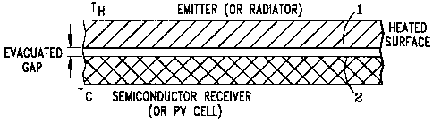
La présente invention concerne un procédé permettant de renforcer la génération des porteurs de charges, tels que les électrons et/ou les trous, dans des semi-conducteurs, tels que des cellules photovoltaïques et similaires, recevant un rayonnement d'une surface chauffée. En l'occurrence, on dispose la surface du semi-conducteur à environ un micron de la surface chauffée, le vide ayant été de préférence réalisé dans l'intervalle entre les deux surfaces.


Abrégé anglais


A technique for enhancing the generation of carriers (ex. Electrons and/or
holes) in semiconductor devices such as photovoltaic cells
and the like, receiving radiation from a heated surface, through the use of
micron juxtaposition of the surface of the device and the heated
surface and with the gap thereinbetween preferably evacuated.

Revendications

Note : Les revendications sont présentées dans la langue officielle dans laquelle elles ont été soumises.


7
CLAIMS:
1. A method of enhancing the generation of carriers in a semiconductor surface
receiving radiation from a heated surface heated to a temperature greater than
the semiconductor surface that comprises, placing the surfaces in
juxtaposition,
and characterised by adjusting the gap between the surfaces to micron scale
separation.
2. A method as claimed in claim 1 wherein the gap is evacuated and the
separation
is adjusted to the order of 0.01 to 100 microns.
3. A method as claimed in claim 2 wherein the semiconductor surface comprises
a
photovoltaic device.
4. A method as claimed in claim 3 wherein the surfaces of the photovoltaic
device
and of the heated surface are substantially planar.
5. A method as claimed in claim 4 wherein one or both of the juxtaposed
surfaces
are patterned.
6. A method as claimed in claim 4 wherein in addition to controlling the
separation
between the surfaces the photovoltaic properties of one or more of the
surfaces
in dimensions orthogonal and parallel to the separation are varied.
7. A method as claimed in claim 1 wherein the radiation is emitted from the
heated
surface of temperature T H and the semiconductor surface is maintained at
temperature T C where T H >T C.

8
8. The method claimed in claim 7 wherein a material is chosen to form one or
both
of the heated and semiconductor surfaces to tailor the spectrum of the emitted
radiation coupled through the gap.
9. The method as claimed in claim 8 wherein said material is provided along
one or
more of the X, Y and Z axes of either or both surfaces.
10. The method as claimed in claim 8 wherein either or both of the surfaces is
provided with one of patterns, channels, islands and three-dimensional forms.
11. The method as claimed in claim 7 wherein the gap between the surfaces is
adjusted is adjusted by controlling the leveling of the surfaces.
12. The method as claimed in claim 7 wherein the gap is isolated from
vibration.
13. The method as claimed in claim 7 wherein the semiconductor surface is
constructed to render it a photovoltaic device.
14. The method as claimed in any one of claims 1 to 13 wherein a thermally
insulative
substantially lossless radiation-transmitting gap is provided in the form of
an
evacuated gap.
15. The method of claim 14 wherein the enhancement in the generation of
carriers
which is achieved by the adjustment of the gap between the surfaces creates
energy stimulation which is converted into enhanced generation of electrical
currents.

9
16. The method of claim 14 wherein the relatively cool surface is a
photovoltaic
surface and the enhanced generation of the electrical currents manifests
itself in
the power output of the photovoltaic surface.
17. A combined radiation transfer and carrier-generating semiconductor
apparatus
having in combination, semiconductor and heat-radiating surfaces means for
maintaining the heat-radiating surface at a temperature greater than that of
the
semiconductor surface, a thermally insulating and substantially lossless
radiation
transmitting gap formed between the surfaces for coupling the radiation from
the
heat-radiating surface for reception by the semiconductor surface;
characterised
by means for adjusting the width of the gap to the order of submicrons/microns
thereby to achieve an enhanced increase in the semiconductor generation of
charged carriers in response to the radiation coupled through the gap.
18. Apparatus as claimed in claim 17 wherein the gap comprises an evacuated
gap,
the width of the gap is adjusted to a separation in the range of 0.01 to 20
microns.

Description

Note : Les descriptions sont présentées dans la langue officielle dans laquelle elles ont été soumises.


CA 02298790 2000-01-28
WO 99/07021 PCT/IB98/01130
THERMOPHOTOVOLTAIC SEMICONDUCTOR DEVICE
The present invention relates to the general area of generating carriers such
as electrons and
holes within semiconductors by the action of incident radiation, being more
particularly
concerned with radiation emanating from heated surfaces, and, in an important
application, to
the enhancement of such generation within photovoltaic devices and the like,
due to the close
proximity of the heated surface.
BACKGROUND OF THE INVENTION
In a common photovoltaic cell, a semiconductor p-n junction is formed close to
the surface of
the semiconductor material that forms the cell. When photons emitted by a
light source such
as the sun impinge on the cell surface, electron-hole pairs are created. These
electron-hole
pairs are separated by the space-charge potential that is a consequence of the
p-n junction.
The net result is a DC current. Thermophotovoltaics operate in a similar
manner except that,
instead of a light source, a surface at a higher temperature than the
semiconductor material
acts as the source of photons. In this case, thermal radiation is the
mechanism of energy
transfer and the temperature of the emitting surface which dictates the
spectral composition of
the radiation must be matched to the material and electronic properties of the
semiconductor
such as its bandgap in order to optimize conversion efficiency.
Prior thermophotovoltaic devices and systems have been designed such that the
distance
between the emitting surface and the cell surface is large relative to the
characteristic
wavelength of the thermal radiation. Hence, the thermal radiation transfer is
characterised by
the Stefan-Boltzman Law and its spectral composition by Planck's law.
CONFIRMATION COPY

CA 02298790 2000-01-28
2
WO 99/07021 PCT/IB98/01130
MICROSCALE RADIATIVE HEAT TRANSFER
Turning now from the field of semiconductor devices, including photovoltaic
cells and the like,
to the general field of radiative heat transfer, in the classical theory of
radiative heat transfer,
the radiated power per area and per interval of wavelength of a flat surface
in thermal
equilibrium with its surrounding is given by Planck's Law. Integration of
Planck's Law over all
wavelengths yields the Stefan-Boltzman Law for black surfaces. Similarly this
law governs the
exchange of energy between two black surfaces.
Planck's Law predicts that a large portion of the radiative energy at a given
temperature of
radiating body will be around the wavelength of greatest spectral intensity
"lambdamax".
"Lambdamax" is predicted by the Wien Displacement Law. At shorter wavelengths
the power
falloff is very rapid whereas at wavelengths greater than lambdamax the
falloff is much more
gradual. At lower temperatures lambdamax occurs at longer wavelengths.
In the above classical theory it is assumed that the distances between
radiating surfaces is
large compared to the wavelengths of the energy involved. Planck himself
imposed this
condition on his derivation. Over the last several decades a small segment of
radiative heat
transfer theory and experiment has developed wherein the spaces between
radiating solids
are on the order of and smaller than the characteristic wavelengths of the
radiation
exchanged. There is experimental evidence to show that energy exchange between
two
surfaces (dielectric to dielectric or metal to metal) separated by a distance
of the same order
as the wavelength or less can be several times larger than at larger
distances, and that the
magnitude of this effect increases sharply with decreasing distance. Examples
of such
experiments are Cravalho, E.G. et. Al., Nov.1967, "Effect of Small Spacings on
Radiative
Transfer Between Dielectrics", Journal of Heat Transfer, pp.351-358;
Hargreaves, C.M., 1973,
"Radiative Transfer Between Closely Spaced Bodies", Philips Res. Reports
Supplement No.5,
pp.1-80; and Kutateladze, S.S. et.al., Aug. 1978, "Effect of Magnitude of Gap
Between Metal

CA 02298790 2006-06-01
3
Plates on their Thermal Interaction at Cryogenic Temperatures", Sov. Phys.
Dokl. 23 (8),
pp. 577-578. Orders of magnitude increase with very small or "microscale"
spacings were
theoretically predicted by Polder, D. et.al., Nov. 1971,"Theory of Radiative
Heat Transfer
Between Closely Spaced Bodies", Physical Review B, Vol. 4, No. 10, pp. 3303-
3314 and
Levin, M. L. et.al., 1980,"Contribution to the Theory of Heat Exchange Due to
a
Fluctuating Electromagnetic Field", Sov. Phys. JETP, Vol. 6, pp. 1054-1063.
Underlying the present invention is my novel conceptual insight and discovery
that these
previously unrelated technologies of thermophotovoltaic energy conversion and
of small
spacing radiative heat transfer systems could synergistically be combined in
such a
manner as to enhance the generation of semiconductor carriers (electrons and
holes) in
semiconductor devices such as photovoltaic cells and the like, receiving
radiation, such
as photons, from a heated surface, through the use of very small gap
juxtaposition of the
surfaces of the device and the heated surface.
OBJECTS OF THE INVENTION
A primary object of the invention accordingly, is to provide a new and
improved method
of enhancing the generation of carriers (ex. Electrons and/or holes) in
semiconductor
devices and near their surfaces, receiving radiation from a heated surface,
through the
use of very small gap ("microscale") juxtaposition of the surface of the
semiconductor
surface or device and the heated surface.
A further object is to provide an improved thermovoltaic system.

CA 02298790 2006-06-01
4
Other and further objects will be explained hereinafter and will be more
particularly
delineated in the appended claims.
SUMMARY
In summary, from one of its broader aspects, the invention embraces a method
of
enhancing the generation of carriers in a semiconductor near its surface
receiving
radiation from a heated surface, that comprises, placing the surfaces in
juxtaposition, and
adjusting the space therebetween to micron scale separation.
More generically, the invention combines previously unrelated technologies of
thermophotovoltaic energy conversion and of small spacing radiative heat
transfer
systems in such a manner as to enhance the generation of semiconductor
carriers.
In accordance with one aspect of the present invention there is provided a
method of
enhancing the generation of carriers in a semiconductor surface receiving
radiation from
a heated surface heated to a temperature greater than the semiconductor
surface that
comprises, placing the surfaces in juxtaposition, and characterised by
adjusting the gap
between the surfaces to micron scale separation. The radiation may be emitted
from the
heated surface of temperature TH and the semiconductor surface may maintained
at
temperature Tc where TH > Tc. A material may be chosen to form one or both of
the
heated and semiconductor surfaces to tailorthe spectrum of the emitted
radiation coupled
through the gap. The submicron/micron thickness of the gap may be adjusted by
controlling the leveling of the surfaces. The gap may be isolated from
vibration. The
semiconductor may be constructed to render it a photovoltaic device.
In accordance with another aspect of the present invention there is provided a
combined
radiation transfer and carrier-generating semiconductor apparatus having in
combination,
semiconductor and heat-radiating surfaces means for maintaining the heat-
radiating
surface at a temperature greater than that of the semiconductor surface, a
thermally

CA 02298790 2006-06-01
insulating and substantially lossless radiation transmitting gap formed
between the
surfaces for coupling the radiation from the heat-radiating surface for
reception by the
semiconductor surface; characterised by means for adjusting the width of the
gap to the
order of submicrons/microns thereby to achieve an enhanced increase in the
5 semiconductor generation of charged carriers in response to the radiation
coupled
through the gap.
Preferred and best mode designs and implementations will later be detailed.
DRAWINGS
The invention will now be described in connection with the accompanying
drawing, the
schematic figure of which illustrates the novel principles of the invention as
applied to an
exemplary application of a thermophotovoltaic device.
PREFERRED EMBODIMENT (S) OF THE INVENTION
Referring to the drawing, a heated surface emitter of radiation, including
photons, is
schematically shown at 1 in the form of a substantially planar hot surface at
temperature
TH, juxtaposed in accordance with the present invention, in very close
proximity to a
substantially parallel surface 2 of a semiconductor receiver of the radiation,
such as a
photovoltaic cell of

CA 02298790 2006-06-01
5a
relatively cool temperature of Tc. Cell current collection contacts and grid
(not shown)
would be provided in the bottom or back surface or recessed from the front
active surface
of the cell.
The enhanced synergistic effect of the invention in terms of significant
increases in carrier
generation in response to the incident radiation from heated surface 1, is
achieved by
effecting the above-mentioned critical close proximity of the surfaces 1 and 2
with a micro
gap (Evacuated Gap) on the order of 0.01 microns up to the order of about 1
micron and
in some cases of longer wavelengths (as in cryogenic applications and the
like) even up
to the order of 100 microns, 0.01-20 microns being a preferred range for most
applications.
The fine adjustment of the crucial micron range separation gap between the
surfaces 1
and 2 may be controlled by such devices as piezoelectric controlled levelling
stages or
the like such as the Model 8095 of New Focus Corporation.
In view of the very small gap, moreover, vibration isolation may be required
as by
conventional isolation tables and the like.
While the invention has been described in connection with the example of a
photovoltaic
semiconductor device, it is evident that the carrier enhancement effect from
close
juxtaposition of a semiconductor surface and a heated surface is generically
applicable
and useful.
Instead of flat surfaces, patterns may be etched or otherwise formed into
three-dimensional forms (channels, islands, etc.) to tailorthe electromagnetic
spectrum
of the radiant energy being transferred to the juxtaposed semiconductor
surface.
There may then be a natural progression from one dimension, MTPV, i. e

CA 02298790 2000-01-28
6
WO 99/07021 PCT/IB98/01130
controlling the distance between two surfaces, to three dimensions wherein in
addition to the
Microscale spacing, the properties of the surfaces as a function of the two
lateral dimensions
are also controlled. In summary, if x and y are in the plane of the Emitter
and Receiver chip
surfaces and z is perpendicular to them, then the degrees of freedom are: z
between the
chips, z within one or both chips, x and y within one or both chips, and x and
y of one chip
relative to the other.
Semiconductors include Si and binary, ternary, and quaternary compound
semiconductors
including lnAs, InGaAs, and InGaAsSb and others
The heated surface, moreover, may, as described in said thesis, not only
involve lattice and
carriers at the same temperature, but also conditions where the carriers are
at a hotter
temperature than the lattice ("hot electrons") as through absorption of
electromagnetic energy.
Further modifications will also occur to those skilled in this art, and such
are considered to fall
within the spirit and scope of this invention as defined in the appended
claims.

Dessin représentatif
Une figure unique qui représente un dessin illustrant l'invention.
États administratifs

2024-08-01 : Dans le cadre de la transition vers les Brevets de nouvelle génération (BNG), la base de données sur les brevets canadiens (BDBC) contient désormais un Historique d'événement plus détaillé, qui reproduit le Journal des événements de notre nouvelle solution interne.

Veuillez noter que les événements débutant par « Inactive : » se réfèrent à des événements qui ne sont plus utilisés dans notre nouvelle solution interne.

Pour une meilleure compréhension de l'état de la demande ou brevet qui figure sur cette page, la rubrique Mise en garde , et les descriptions de Brevet , Historique d'événement , Taxes périodiques et Historique des paiements devraient être consultées.

Historique d'événement

Description Date
Inactive : Périmé (brevet - nouvelle loi) 2018-07-27
Inactive : CIB expirée 2014-01-01
Exigences relatives à la nomination d'un agent - jugée conforme 2012-10-25
Inactive : Lettre officielle 2012-10-25
Exigences relatives à la révocation de la nomination d'un agent - jugée conforme 2012-10-25
Demande visant la révocation de la nomination d'un agent 2012-10-18
Demande visant la nomination d'un agent 2012-10-18
Inactive : TME en retard traitée 2012-06-19
Lettre envoyée 2011-07-27
Inactive : TME en retard traitée 2010-07-27
Lettre envoyée 2009-07-27
Accordé par délivrance 2009-03-24
Inactive : Page couverture publiée 2009-03-23
Préoctroi 2009-01-05
Inactive : Taxe finale reçue 2009-01-05
Un avis d'acceptation est envoyé 2008-11-12
Lettre envoyée 2008-11-12
Un avis d'acceptation est envoyé 2008-11-12
Inactive : CIB en 1re position 2008-11-07
Inactive : CIB attribuée 2008-11-07
Inactive : Approuvée aux fins d'acceptation (AFA) 2008-07-30
Modification reçue - modification volontaire 2006-06-01
Inactive : Dem. de l'examinateur art.29 Règles 2005-12-05
Inactive : Dem. de l'examinateur par.30(2) Règles 2005-12-05
Lettre envoyée 2005-08-31
Exigences de rétablissement - réputé conforme pour tous les motifs d'abandon 2005-08-15
Réputée abandonnée - omission de répondre à un avis sur les taxes pour le maintien en état 2005-07-27
Lettre envoyée 2005-07-19
Exigences de rétablissement - réputé conforme pour tous les motifs d'abandon 2005-06-30
Lettre envoyée 2004-08-12
Réputée abandonnée - omission de répondre à un avis sur les taxes pour le maintien en état 2004-07-27
Exigences de rétablissement - réputé conforme pour tous les motifs d'abandon 2004-07-26
Lettre envoyée 2003-08-25
Réputée abandonnée - omission de répondre à un avis sur les taxes pour le maintien en état 2003-07-28
Toutes les exigences pour l'examen - jugée conforme 2003-07-24
Exigences pour une requête d'examen - jugée conforme 2003-07-24
Requête d'examen reçue 2003-07-24
Lettre envoyée 2002-09-05
Exigences de rétablissement - réputé conforme pour tous les motifs d'abandon 2002-08-21
Réputée abandonnée - omission de répondre à un avis sur les taxes pour le maintien en état 2002-07-29
Lettre envoyée 2001-08-30
Exigences de rétablissement - réputé conforme pour tous les motifs d'abandon 2001-08-17
Réputée abandonnée - omission de répondre à un avis sur les taxes pour le maintien en état 2001-07-27
Inactive : Page couverture publiée 2000-03-30
Inactive : CIB en 1re position 2000-03-29
Inactive : Notice - Entrée phase nat. - Pas de RE 2000-03-14
Demande reçue - PCT 2000-03-13
Déclaration du statut de petite entité jugée conforme 2000-01-28
Demande publiée (accessible au public) 1999-02-11

Historique d'abandonnement

Date d'abandonnement Raison Date de rétablissement
2005-07-27
2004-07-27
2003-07-28
2002-07-29
2001-07-27

Taxes périodiques

Le dernier paiement a été reçu le 2008-06-17

Avis : Si le paiement en totalité n'a pas été reçu au plus tard à la date indiquée, une taxe supplémentaire peut être imposée, soit une des taxes suivantes :

  • taxe de rétablissement ;
  • taxe pour paiement en souffrance ; ou
  • taxe additionnelle pour le renversement d'une péremption réputée.

Veuillez vous référer à la page web des taxes sur les brevets de l'OPIC pour voir tous les montants actuels des taxes.

Historique des taxes

Type de taxes Anniversaire Échéance Date payée
Taxe nationale de base - petite 2000-01-28
TM (demande, 2e anniv.) - petite 02 2000-07-27 2000-07-19
TM (demande, 3e anniv.) - petite 03 2001-07-27 2001-08-17
Rétablissement 2001-08-17
TM (demande, 4e anniv.) - petite 04 2002-07-29 2002-08-21
Rétablissement 2002-08-21
Requête d'examen - petite 2003-07-24
Rétablissement 2004-07-26
TM (demande, 5e anniv.) - petite 05 2003-07-28 2004-07-26
2004-07-26
2005-06-30
Rétablissement 2005-06-30
TM (demande, 6e anniv.) - petite 06 2004-07-27 2005-06-30
Rétablissement 2005-08-15
2005-08-15
TM (demande, 7e anniv.) - petite 07 2005-07-27 2005-08-15
TM (demande, 8e anniv.) - petite 08 2006-07-27 2006-06-12
2006-06-12
TM (demande, 9e anniv.) - générale 09 2007-07-27 2007-07-04
TM (demande, 10e anniv.) - générale 10 2008-07-28 2008-06-17
Taxe finale - générale 2009-01-05
TM (brevet, 11e anniv.) - générale 2009-07-27 2010-07-27
TM (brevet, 12e anniv.) - générale 2010-07-27 2010-07-27
Annulation de la péremption réputée 2011-07-27 2010-07-27
Annulation de la péremption réputée 2011-07-27 2012-06-19
TM (brevet, 13e anniv.) - générale 2011-07-27 2012-06-19
TM (brevet, 14e anniv.) - générale 2012-07-27 2012-07-16
TM (brevet, 15e anniv.) - générale 2013-07-29 2013-07-17
TM (brevet, 16e anniv.) - générale 2014-07-28 2014-07-09
TM (brevet, 17e anniv.) - générale 2015-07-27 2015-07-01
TM (brevet, 18e anniv.) - générale 2016-07-27 2016-07-06
TM (brevet, 19e anniv.) - générale 2017-07-27 2017-06-28
Titulaires au dossier

Les titulaires actuels et antérieures au dossier sont affichés en ordre alphabétique.

Titulaires actuels au dossier
ROBERT STEPHEN DIMATTEO
Titulaires antérieures au dossier
S.O.
Les propriétaires antérieurs qui ne figurent pas dans la liste des « Propriétaires au dossier » apparaîtront dans d'autres documents au dossier.
Documents

Pour visionner les fichiers sélectionnés, entrer le code reCAPTCHA :


Pour visualiser une image, cliquer sur un lien dans la colonne description du document. Pour télécharger l'image (les images), cliquer l'une ou plusieurs cases à cocher dans la première colonne et ensuite cliquer sur le bouton "Télécharger sélection en format PDF (archive Zip)" ou le bouton "Télécharger sélection (en un fichier PDF fusionné)".

Liste des documents de brevet publiés et non publiés sur la BDBC .

Si vous avez des difficultés à accéder au contenu, veuillez communiquer avec le Centre de services à la clientèle au 1-866-997-1936, ou envoyer un courriel au Centre de service à la clientèle de l'OPIC.


Description du
Document 
Date
(aaaa-mm-jj) 
Nombre de pages   Taille de l'image (Ko) 
Dessin représentatif 2000-03-30 1 8
Description 2000-01-28 6 246
Abrégé 2000-01-28 1 47
Revendications 2000-01-28 4 149
Dessins 2000-01-28 1 12
Page couverture 2000-03-30 1 36
Revendications 2006-06-01 3 79
Description 2006-06-01 7 260
Dessin représentatif 2008-09-15 1 10
Page couverture 2009-03-02 1 36
Rappel de taxe de maintien due 2000-03-28 1 111
Avis d'entree dans la phase nationale 2000-03-14 1 193
Courtoisie - Lettre d'abandon (taxe de maintien en état) 2001-08-27 1 185
Avis de retablissement 2001-08-30 1 172
Courtoisie - Lettre d'abandon (taxe de maintien en état) 2002-08-26 1 182
Avis de retablissement 2002-09-05 1 170
Rappel - requête d'examen 2003-03-31 1 120
Accusé de réception de la requête d'examen 2003-08-25 1 173
Courtoisie - Lettre d'abandon (taxe de maintien en état) 2003-08-25 1 176
Avis de retablissement 2004-08-12 1 165
Courtoisie - Lettre d'abandon (taxe de maintien en état) 2004-09-21 1 178
Avis de retablissement 2005-07-19 1 165
Courtoisie - Lettre d'abandon (taxe de maintien en état) 2005-08-31 1 173
Avis de retablissement 2005-08-31 1 165
Avis du commissaire - Demande jugée acceptable 2008-11-12 1 164
Avis concernant la taxe de maintien 2009-09-08 1 171
Quittance d'un paiement en retard 2010-08-17 1 163
Avis concernant la taxe de maintien 2011-09-07 1 170
Quittance d'un paiement en retard 2012-06-19 1 165
PCT 2000-01-28 14 536
Taxes 2002-08-21 1 34
Taxes 2001-08-17 1 39
Taxes 2004-07-26 1 34
Taxes 2005-06-30 1 35
Taxes 2005-08-15 1 35
Correspondance 2009-01-05 1 31
Taxes 2010-07-27 1 35
Correspondance 2012-10-18 2 74
Correspondance 2012-10-25 1 13
Correspondance 2012-10-25 1 16