Note : Les descriptions sont présentées dans la langue officielle dans laquelle elles ont été soumises.
CA 02298868 2000-02-15
Doc. No 10-140 CA (2) Patent
Configurable Optical Circuit
Field of the Invention
This invention relates generally to the field of demultiplexing and more
particularly
relates to a configurable optical circuit for directing and/or multiplexing
and/or
demultiplexing optical signals to particular locations.
Background of the Invention
Using optical signals as a means of carrying channeled information at high
speeds
through an optical path such as an optical waveguide i.e. optical fibres, is
preferable over
other schemes such as those using microwave links, coaxial cables, and twisted
copper
wires, since in the former, propagation loss is lower, and optical systems are
immune to
t 5 Electro-Magnetic Interference (EMI), and have higher channel capacities.
High-speed
optical systems have signaling rates of several mega-bits per second to
several tens of
giga-bits per second.
Optical communication systems are nearly ubiquitous in communication networks.
The
2o expression herein "Optical communication system" relates to any system that
uses optical
signals at any wavelength to convey information between two points through any
optical
path. Optical communication systems are described for example, in Gower, Ed.
Optical
communication Systems, (Prentice Hall, NY) 1993, and by P.E. Green, Jr in
"Fiber optic
networks" (Prentice Hall New Jersey) 1993, which are incorporated herein by
reference.
As communication capacity is further increased to transmit an ever-increasing
amount of
information on optical fibres, data transmission rates increase and available
bandwidth
becomes a scarce resource.
CA 02298868 2000-02-15
Doc. No 10-140 CA (2) Patent
High speed data signals are plural signals that are formed by the aggregation
(or
multiplexing) of several data streams to share a transmission medium for
transmitting
data to a distant location. Wavelength Division Multiplexing (WDM) is commonly
used
in optical communications systems as means to more efficiently use available
resources.
In WDM each high-speed data channel transmits its information at a pre-
allocated
wavelength on a single optical waveguide. At a receiver end, channels of
different
wavelengths are generally separated by narrow band filters and then detected
or used for
further processing. In practice, the number of channels that can be carried by
a single
optical waveguide in a WDM system is limited by crosstalk, narrow operating
bandwidth
~ o of optical amplifiers and/or optical fiber non-linearities. Moreover such
systems require
an accurate band selection, stable tunable lasers or filters, and spectral
purity that increase
the cost of WDM systems and add to their complexity. This invention relates to
a
method and system for filtering or separating closely spaced channels that
would
otherwise not be suitably filtered by conventional optical filters. A
significant part of this
invention relates to a system wherein an optical system can be dynamically
configured
and controlled to route optical signals to particular destinations. In one
aspect of the
invention a configurable add/drop circuit is provided which allows
inexpensive, "sloppy"
filters having poor slopes and responses to be used by first demultplexing
closely spaced
wavelengths corresponding to adjacent optical channels by the use of a de-
interlever
2o filter for example such the one described in U.S. Patent application number
08/864,895
assigned to the same assignee. This invention is not limited to de-
interleavers which de-
interleave or interleave every alternate channel into two data streams, but
includes de-
interleavers/interleaver which demultiplex into several streams of further
spaced
channels, as for example, shown in Fig. 15.
Currently, internationally agreed upon channel spacing for high-speed optical
transmission systems, is 100 Ghz, equivalent to 0.8 nm spacing between centre
wavelengths of adjacent channels, surpassing, for example 200 Ghz channel
spacing
equivalent to 1.6 nanometers between centre wavelengths between adjacent
channels. Of
3o course, as the separation in wavelength between adjacent channels
decreases, the
2
CA 02298868 2000-02-15
Doc. No 10-140 CA (2) Patent
requirement and demand for more precise demultiplexing circuitry capable of
ultra-
narrow-band filtering, absent crosstalk, increases. With the available
technology of
today, the use of conventional dichroic filters to separate channels spaced by
0.4 nm or
less without crosstalk, is not practicable; such filters being difficult if
not impossible to
manufacture.
It is an object of one aspect of this invention to utilize a circuit for
separating an optical
signal having closely spaced channels into at least two optical signals
wherein channel
spacing between adjacent channels is greater in each of the at least two
optical signals,
~ o thereby requiring less precise filters to demultiplex channels carried by
each of the at
least two signals. It is a further object of this invention to provide a
dynamically
configurable add/drop circuit for adding or dropping demultiplexed data
channels.
Summary of the Invention
In accordance with this invention a new, enabling, de-
interleaving/interleaving
technology that can be integrated with known DWDM components is provided,
yielding
a very high performance modular device having narrow channel spacing and high
channel count. These new combined devices in accordance with this invention
exhibit
excellent performance characteristics including low loss, low crosstalk, high
isolation,
2o uniform channel response and superior channel accuracy with reduced
temperature
sensitivity. The device in accordance with this invention can be applied
directly to
established systems to increase the channel count and allow the use of reduced
channel
spacing.
In accordance with this invention, a configurable optical system is provided
comprising:
a first de-interleaver/interleaver demultiplexing /multiplexing circuit,
having at least an
input port for receiving an optical signal having a plurality of multiplexed
channels of
light, and having a plurality of output ports for receiving demultiplexed
channels of light;
a second de-interleaver/interleaver multiplexing/demultiplexing circuit
optically coupled
3o with the first interleaver demultiplexing /multiplexing circuit and having
a plurality of
3
CA 02298868 2000-02-15
Doc. No 10-140 CA (2) Patent
light receiving ports and at least an output port for receiving a multiplexed
optical signal,
and;
a controller for dynamically controlling the direction of at least one
wavelength band of
light propagating between the first and second de-interleaver/interleaver
circuits in
dependence upon at least a control signal.
In accordance with another aspect of the invention, a configurable optical
system is
provided comprising:
a first de-interleaver/interleaver demultiplexing /multiplexing circuit,
having at least an
to input port for receiving an optical signal having a plurality of
multiplexed channels of
light, and having a plurality of output ports for receiving demultiplexed
channels of light;
a second de-interleaver/interleaver multiplexing/demultiplexing circuit
optically coupled
with the first interleaver demultiplexing /multiplexing circuit and having a
plurality of
light receiving ports and at least an output port for receiving a multiplexed
optical signal,
l5 and;
direction control circuitry for directing at least one wavelength band of
light propagating
between the first and second interleaver circuits in dependence upon at least
a control
signal.
2o In accordance with another aspect of the invention there is provided, an
integrated
reconfigurable add and / or drop optical system comprising:
a first integrated waveguide block having integrated waveguides therein, said
first block
for providing a plurality of de-interleaved channels at a plurality of ports;
a second integrated waveguide block optically coupled with the plurality of
ports of the
25 first integrated waveguide block, the second block having a plurality of
tunable gratings
therein for directing particular channels towards an output port or towards a
drop port;
a third integrated waveguide block having integrated waveguides therein, said
third block
for receiving at least some of the de-interleaved channels and for
interleaving and
directing said channels to the output port.
4
CA 02298868 2000-02-15
Doc. No 10-140 CA (2) Patent
Brief Description of the Drawings
Exemplary embodiments of the invention will now be described in conjunction
with the
drawings, in which:
Fig. 1 is a graph of an output response for two dichroic mufti-layer filters
centered at two
wavelengths in a 200 Ghz system;
Fig. 2 is a circuit block diagram of an interleaves circuit used in an aspect
of this
invention;
Fig. 3 is a graph of an output response for a single etalon showing
transmission and
~ o reflection versus wavelength;
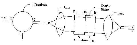
Fig. 3a is a diagram of the etalon depicted in Fig. 3;
Fig. 4 is a graph of an output response for a single etalon showing
transmission and
reflection versus wavelength;
Fig. 4a is a diagram of the etalon depicted in Fig. 4;
Fig. 5 is a graph of an output response for a single etalon showing
transmission and
reflection versus wavelength;
Fig. Sa is a diagram of the etalon depicted in Fig. 5;
Fig. 6 is a graph of an output response for a single etalon showing
transmission and
reflection versus wavelength;
2o Fig. 6a is a diagram of the etalon depicted in Fig. 6;
Fig. 7 is a graph of an output response for a single etalon showing
transmission and
reflection versus wavelength;
Fig. 7a is a diagram of the etalon depicted in Fig. 7;
Figs 7b and 7c are more detailed diagrams of the devices used in accordance
with an
aspect of this invention;
Fig. 8 is an optical circuit diagram of a sub-system for demultiplexing one
high density
channelized optical signal into two less dense optical signals;
Fig. 9 is an optical circuit diagram of a system used in accordance with an
aspect of this
invention;
5
CA 02298868 2000-02-15
Doc. No 10-140 CA (2) Patent
Fig. 10 is an optical circuit diagram of a system used in accordance with an
aspect of this
- invention;
Fig. 11 a is an optical circuit diagram of a system used in accordance with an
aspect of
this invention;
Fig. 11 b is an optical circuit diagram of a system used in accordance with an
aspect of
this invention;
Fig. 12 is a circuit block diagram of a configurable optical circuit in
accordance with this
invention;
Fig. 13 is schematic block diagram of a portion of the circuit shown in Fig.
12 including a
to a control circuit block;
Fig. 14 is an optical circuit diagram of an alternative embodiment of a
portion of the
circuit shown in Fig. 12, in accordance with this invention;
Fig. 15 is a block circuit diagram of a waveguide chip for monitoring
wavelengths in
accordance with this invention;
Fig. 16 is a block diagram showing four waveguide chips in accordance with an
aspect of
the invention;
Figs 17a and 17b are optical circuit diagrams depicting a first and second
circuit
respectively for demultiplexing wavelengths, the preferred circuit being the
second
circuit; and,
2o Fig. 18 is a schematic diagram of a system similar to the one shown in Fig.
12.
Detailed Description
Referring now to Fig. l, wavelength responses 10 and 20 for two filters
designed to pass
two adjacent channels centered at ~,1 and ~.2 respectively, are shown. The
filters are
designed to operate with a 200 Ghz optical system, wherein the distance
between center
wavelengths of adjacent channels is 1.6 nm. The filter's responses 10 and 20
are shown
to have boundaries indicated by dashed lines within which each laser providing
a data
signal for each channel may operate. Thus, for example, a laser that operates
to provide
3o the optical data signal of channel 1, corresponding to filter response 10,
must operate
6
CA 02298868 2000-02-15
Doc. No 10-140 CA (2) Patent
between wavelengths corresponding to lines l0a and 1 Ob, and in a same manner
the laser
that provides the optical signal for channel 2, must operate to provide an
optical data
signal that has a wavelength that is between the dashed lines 20a and 20b.
In order for the optical system to operate so that the integrity of the data
is preserved,
crosstalk between adjacent channels must be minimized and must at least be
below a
predetermined allowable maximum level (-20 dB). In Fig. 1, the response of
filter 20 is
shown to overlap with the response of filter 10, the overlap region indicated
by the cross-
hatched triangular region 40. Furthermore, the dashed line l Ob is shown to
intersect the
1 o sloped line indicating the response of the filter 10, at a point 50. Thus,
if the distance (or
channel spacing) between dashed lines l Ob and 20a was lessened, i.e. in order
to have a
more dense communication system by increasing the number of total channels for
a given
bandwidth, cross talk between adjacent channels would exceed allowable maximum
level
(-20 dB) using the filters shown.
When 100 Ghz channel spacing equivalent to 0.8 nm is implemented, the filters
depicted
by the output responses 10 and 20 do not adequately separate channels 1 and 2
and high
levels of crosstalk adversely affect data retrieval. In this instance,
conventional dichroic
filters as shown in Fig. l, would not suffice and crosstalk would exceed
allowable
2o maximum levels.
One aspect of this invention utilizes an optical circuit for first
demultiplexing a channeled
optical signal, that is, a signal comprising multiplexed closely spaced
channels, into a
plurality of less-dense channeled signals each comprising a plurality of
multiplexed less
closely spaced channels. In a first direction wherein the circuit performs a
multiplexing
function on a plurality of channels launched into a first end of the circuit,
it is an
interleaver circuit, and in an opposite direction wherein the circuit performs
a
demultiplexing function on a composite signal launched therein at an opposite
end to
provide a plurality of demultiplexed channels it serves as a de-interleaver
circuit.
3o However, the term interleaver circuit shall be used hereafter to denote
this interleaver/de-
7
CA 02298868 2000-02-15
Doc. No 10-140 CA (2) Patent
interleaves circuit. One such interleaves circuit is disclosed as a comb
splitting filter in
U.S. Patent No. 5,680,490 in the name of Cohen.
Referring now to Fig. 2, an optical interleaves circuit is shown including a 3-
port optical
circulator having an input port 101, its second port 102 coupled with a Fabry-
Perot etalon
filter 110, and a third port 103 serving as an output port. The Fabry-Perot
etalon filter
110 has two partially reflective mirrors, or surfaces, facing each other and
separated by a
certain fixed gap which forms a resonant optical cavity.
t o In general, the spectral characteristics of an etalon filter are
determined by the reflectivity
of the mirrors or reflective surfaces and the length of the gap or space
between the
mirrors or reflective surfaces. The Fabry-Perot principle allows a wideband
optical beam
to be filtered whereby only periodic spectral passbands are substantially
transmitted out
of the filter. Conversely, if the reflectivity of the mirrors or reflective
surfaces are
selected appropriately, periodic spectral passbands shifted by d nanometers
are
substantially reflected backwards from the input mirror surface. In adjustable
Fabry-
Perot devices, such as one disclosed in United States Patent number 5,283,845
in the
name of Ip, assigned to JDS Fitel Inc., tuning of the center wavelength of the
spectral
passband is achieved typically by varying the effective cavity length
(spacing).
Referring now to Figs. 3, 4, 5, 6, 7, and 3a, 4a, Sa, 6a, and 7a output
response curves of
five different Fabry-Perot etalon devices 113, 114, 115, 116, and 117 are
shown and
described, in order of their performance, from least to most optimal. Fig. 3
shows an
output response curve for a 2-mirror etalon having an FSR of 1.6 nm and a
finesse of 1.5.
A first curve shown as a solid line is a periodic transmission response in dBs
for the
single etalon 113 to input light ranging in wavelength from 1548 nm to 1552
nm. The
second group of curves in the same figure, shown as dotted lines, depict the
reflection
response of same etalon 113 within the same wavelength range. It is noted that
at the
wavelengths ~,1 1549.2 nm and ~,3 ~ 1550.85 nm the intensity of the reflected
light from
3o the input light launched into the etalon is attenuated by approximately -
3dB. It is further
s
CA 02298868 2000-02-15
Doc. No 10-140 CA (2) Patent
noted that at the wavelengths ~,2 ~ 1550 nm and ~,4 1551.6 nm, essentially all
of the
input light launched into the etalon is transmitted through the 2 mirrors to
the output port
of the etalon 113. Since the etalon is to be used to pass and reflect adjacent
channels
having a 0.4 nm bandwidth, it is preferred that the response of the etalon, in
this instance,
at the wavelengths 7~2 and ~,4, have a window of at least 0.4 nm where
reflection does
not exceed about -25 dB. Stated in more general terms, it is preferred that at
wavelengths
~,1 and 7~3 most of the light incident upon the input port of the etalon is
reflected
backwards, and that most of the light at wavelengths ~,2 and ~,4 be
transmitted through
the etalon. However, as can be seen from the graph of Fig. 3, the transmission
window at
t o ~,2 or 1550 nm, is only 0.06 nm wide at -23 dB. At wavelengths ~,1 and
~,3, and within a
0.4 nm window, approximately half or more of the input light launched into the
etalon is
reflected indicated by the response curve at 3.2dB. The periodicity of the
etalon allows
multiple wavelengths of light to be routed through the device and multiple
other adjacent
wavelengths to be reflected backwards, thereby separating the multiplexed
channelized
input light signal into two less dense optical signals.
Referring now to Fig. 4, a response curve for a 3-mirror two-cavity etalon 114
is shown
having an FSR of 1.6 nm and a reflectivity of R1=0.05 where R2=4R1/(1+R1)2 .
The
mirrors are arranged such that the mirror having a reflectivity R2 is
sandwiched between
2o and spaced a distance d from outer mirrors having a reflectivity R1. It is
noted by the
response curves for this device that at wavelengths ~,1 and ~,3, reflection is
at -2.84 dB
thereby indicating less attenuation of channels at these wavelengths than for
the etalon
113. Furthermore, the transmission window at -23 dB for channels corresponding
to
wavelengths 7~2 and 7~3 is 0.27 nm, again an improvement over the response of
single
cavity etalon 113. Notwithstanding, the etalon 114 does not provide enough
isolation
between adjacent channels.
In Fig. 5, a response curve for 2 3-mirror two-cavity etalons 115 is shown in
reflection
mode; each etalon has an FSR of 1.6 nm and a reflectivity of R1=0.1. In this
9
CA 02298868 2000-02-15
Doc. No 10-140 CA (2) Patent
configuration light is launched into a first etalon 115 and a signal reflected
from the first
etalon 115 is reflected again from the second etalon 115. The window is
approximately
.42 nm for each etalon at 10 dB from the peak for channels corresponding to
wavelengths
7~2 and ~,4, thus providing a window of approximately 0.42 nm for rejection of
~,2 and 7~4
from the reflected signal for the double pass.
Fig. 6 shows a response curve for a 2-pass transmission system having two
double-cavity
etalons with R1=0.21. In this instance channels corresponding to wavelengths
~,1 and 7~3
are substantially blocked within a 0.4 nm window for each etalon 116 and
nearly 100
1 o percent transmission is provided for wavelengths ~,2 and ~,4, with
acceptable levels of
crosstalk from adjacent channels 1 and 3 substantially blocked, corresponding
to
(reflected) wavelengths ~,1 and ~,3. For this configuration care must be taken
to avoid
multiple reflections between the two etalons 116, which would degrade the
performance.
This can be accomplished by passing the optical beam through 166 at a small
angle, or by
~ 5 placing an optical isolator between the two etalons 116.
Turning now to Fig. 7 the response curves for an etalon 117 having 4 mirrors,
wherein
R1=0.2 and R2=0.656 spaced from each other by a distance s. In this embodiment
having multi-cavity etalons defined by a 4-mirror configuration wherein
R1=0.2, and
2o R2=0.656, the response is yet improved over the previous etalon designs. In
this instance,
and as can be seen with reference to Fig. 7. Channels ~,1 and ~.3 are
substantially blocked
over a range of approximately 0.40 nm at -19.8 dB, and there is a transmission
window
of approximately 0.40 nm at -1 dB for channels ~,2 and ~,4. In reflection,
channels ~,1 and
7~3 are almost completely reflected, and ~,2 and ~,4 are largely absent from
the reflected
25 signal, although additional filtering may be necessary to remove remaining
levels of ~.2
and ~,4 from the reflected signal.
By providing mufti-cavity etalon structures, the response is considerably
improved over
that of a single cavity etalon.
CA 02298868 2000-02-15
Doc. No 10-140 CA (2) Patent
By using a device having a periodic response, such as the etalon 116 or 117,
channels 1,
3, S, ...corresponding to wavelengths of light ~,1, ~,3, 7~5, ... are
substantially separated
from adjacent closely spaced channels 2, 4, 6, ....corresponding to
wavelengths of light
~,2, ~,4, ~,6, ... the latter corresponding to wavelengths or channels
transmitted through the
device, and the former corresponding to wavelengths or channels reflected from
etalon
backwards to the input port end of the device and into a waveguide attached
thereto. The
optical circuit shown in Fig. 2 shows an optical circulator as a means of
coupling an
optical signal having closely spaced channels into and out of a Fabry-Perot
etalon,
1o however, other coupling means may be envisaged such as a 50/50 splitter, or
separate
fibers for input signals and reflected output signals. Essentially the means
must allow
light to be launched into the etalon, and for the light to be ported out of
the etalon at its
input port end via reflections backwards, or ported out of the etalon at its
output port end
via transmission through the etalon. Although the circuit in accordance with
this
~ 5 invention is well suited to separating alternate channels from a sequence
of closely
spaced channels, into two optical signals for further filtering and
processing, the circuit is
also suited to separating any plurality of channels that are spaced by a
predetermined
distance or multiple thereof. For example in a system where sequentially
spaced channels
spaced by a distance from one another by 0.8 nm and wherein wavelengths of
light ~,1,
20 ~,2, ~,5,~,6,~,7 are multiplexed into a single optical signal corresponding
to channels
1,2,5,6, and 7, wavelengths ~,1,~,3, ~,5 and 7~7 are separated into a first
optical signal, and
a second optical signal comprises wavelengths ~,2 , ~,4 and a~6 after being
launched into
the etalon 110, having a free spectral range of 1.6 nm. Since a portion of
channels 1, 3, S,
and 7 are passed through the etalon with channels 2, 4, 6 and 8, further
processing will be
25 required to demultiplxed channels 2, 4, 6, and 8.
Turning now to Fig. 8 in conjunction with the etalon shown in Fig. 3 or Fig.
4, a
sub-system is shown, for demultiplexing a composite optical signal carrying
channels 1,
2, 3, 4, ... 8 into a first signal carrying channels 1, 3, 5, 7 and a second
signal carrying
CA 02298868 2000-02-15
Doc. No 10-140 CA (2) Patent
channels 2, 4, 6, and 8. This sub-system may be a part of larger
communications system.
- By way of example, and for the purpose of this description, the etalons for
use in this
system are those shown and described in Fig. 7. At a first end of the sub-
system is an
optical fibre 80 carrying the composite optical signal. An output end of the
optical fibre
80 is coupled to an input port 1 of an optical circulator 82. Coupled to a
next sequential
circulating port 2 is a Fabry-Perot etalon 117 in accordance with this
invention as is
described heretofore. An output port of the etalon 117 is coupled to
conventional filter
means (not shown) for separating channels 2, 4, 6, and 8. Port 3 of circulator
82 is
connected to a second etalon 117a having a same FSR but its output response
shifted by d
~ o to ensure that channels 2, 4, 6, and 8 are fully removed. Further
conventional filter means
in the form of a plurality of dichroic filters 92 are provided for separating
channels 1, 3,
5, and 7.
The operation of the sub-system of Fig. 8 is as follows. A light beam
comprising
channels 1, 2, 3, ... 8 corresponding to wavelengths centered at wavelengths
~,1..~,8 is
launched into the optical fibre 80 and enters port I of the optical circulator
82 exiting port
2 toward the first Fabry Perot etalon 117 at port 2. Light reflected from 117
propagates
to port 3 of circulator 82 and then is passed to etalon I 17a and is
demultiplexed further
with conventional WDM devices 92 and can optionally be amplified. Etalon 117
2o essentially reflects wavelengths of light ~,1, ~,3, ~,5, and ~,7 and
transmits virtually all of
wavelengths ~,2, ~,4, ~,6, and ~,8. It should be understood here that when
wavelengths
such as ~,1, ~,2, ~,3, ~,4.... are described, it is in fact a narrow
predetermined band of
wavelengths about these centre wavelengths, each band comprising a respective
channel,
that is being referred to. However, the reflection from etalon 117 contains
slightly higher
than acceptable levels of light of wavelengths ~,2, ~,4, ~,6, and ~,8. A
second etalon 117a is
required to remove remaining levels of light of wavelengths 7~2, ~,4, ~,6, and
~,8, to avoid
interference with the signals of wavelengths ~,I, ~,3, ~,5, and ~,7.
12
CA 02298868 2000-02-15
Doc. No 10-140 CA (2) Patent
Fig 10 is similar to Fig. 9, except that two reflections from each etalon 115
are required
in order to achieve sufficient isolation. To meet this end, 4-port circulators
are used
which replace the 3-port circulators described heretofore.
Fig. 1 la shows a sub-system using a SO/SO splitter to divide the input
optical signal
between two optical fibers. In the upper optical fiber, two etalons 116
transmit only light
of wavelengths ~,2, 7~4, ~,6, and ~,8. In the lower fiber, two etalons 116a
transmit only
~,1, 7~3, ~,5, and ~,7.
1 o Fig. 11 b shows another configuration where the reflected signal from 116
is used to
obtain light corresponding to channels l, through 7 having centre wavelengths
~,1, 7~3, ~5,
and ~,7 eliminating the 3 dB loss of the 50/50 splitter. As shown the
reflected signal is
captured in a separate optical fiber. Alternatively, an optical circulator may
be used.
~ 5 Referring now to Fig. 12, a configurable optical add-drop circuit is shown
in accordance
with this invention. The circuit 120 includes a first interleaves circuit 122a
having an
input waveguide 124 for receiving channels 1 through 6 having respective
centre
wavelengths 7~1 through ~,6. Output waveguide 126a receives channels 1, 3, and
5 for
provision to a first optical circulator 128a and output waveguide 126b
receives channels
20 2, 4, and 6 for provision to a second optical circulator 128b. The first
circulator 128a is
optically coupled with a second interleaves circuit 122b via a waveguide 134a
having
tunable Bragg gratings 1, 3, and S disposed therein for reflecting or passing
any of
channels 1, 3, or 5. The second circulator 128b is optically coupled with a
second
interleaves circuit 122b via a waveguide 134b having tunable Bragg gratings 2,
4, and 6
25 disposed therein for reflecting or passing any of channels 2, 4, or 6. Add
ports 136a and
136b are optically coupled to waveguides 134a and 134b respectively for adding
new
signals into the circuit. Port 3 of each of the optical circulators 128a and
128b serves as
an output port or "drop" port.
13
CA 02298868 2000-02-15
Doc. No 10-140 CA (2) Patent
The circuit 120 operates in the following manner. A composite input signal is
launched
into waveguide 124 and the first interleaves circuit 122a demultiplexes/de-
interleaves the
composite signal into two data streams; a first data stream consisting of
channels l, 3,
and 5 is directed onto waveguide 126a; and, a second data stream consisting of
channels
2, 4, and 6 is directed onto waveguide 126b. The operation of the optical
circulators and
Bragg gratings is essentially the same, however the combination of first
circulator 128a
and gratings 1, 3, and 5 and associated control circuitry controls the flow
and direction of
channels 1, 3, and 5 wherein the combination of the second circulator 128b and
the
gratings 2, 4, and 6 and associated control circuitry controls the flow and
direction of
~ o channels 2, 4, and 6. In operation, the data stream consisting of channels
1, 3 and 5 is
received by a first port of the optical circulator 128a and is circulated to a
second port
where the signal is directed to the tunable Bragg gratings 1, 3, and 5. For
example, when
tunable Bragg grating 1 is tuned to reflect a centre wavelength ~,1,
wavelengths within
the wavelength band of channel 1 are reflected backwards and re-enter port 2
of the
circulator 128a and are circulated to port 3 of the same circulator. Port 3
serves as a drop
port and channel 1 is dropped at the port labeled OUT1. In the instance that
the gratings
3 and 5 are tuned to pass wavelengths centred at 7~3 and ~,5 respectively,
channels 3 and 5
are passed through waveguide 134a and are directed into the interleaves
circuit 130 which
multiplexes all input signals into a single composite output signal on
waveguide 130.
2o Tunable Bragg gratings are well known, and can be tuned by various means.
For example
applying a heater to a grating will change its period and will alter its
centre (reflective)
wavelength. Alternatively, but less preferably, gratings can be tuned by
stretching or
compressing them. Advantageously, since the input signal comprising channels 1
through
6 is separated in such a manner as to have each adjacent wavelength routed to
a different
waveguide, the demultiplexed streams comprising channels 1, 3, and 5; and,
channels 2,
4, and 6 require less precise gratings to further demultiplex these data
streams. Since
channel 2 has been removed in the data stream on waveguide 126a, there is
space
between channels 1 and 3 which allows "sloppy" less steep, and less costly
filters to be
used.
14
CA 02298868 2000-02-15
Doc. No 10-140 CA (2) Patent
Waveguides 136a and 136b provide a means of launching new channels 1, 3, 5 or
2, 4, 6
respectively into the system. Alternatively other channels having other
central
wavelengths can be added via these waveguides. Thus, Fig. 12 illustrates that
by
launching a plurality of channelized wavelengths into the circuit 120,
particular channels
can be dropped, or added, or passed through. Control circuitry for controlling
the centre
wavelengths of the Bragg gratings is not shown in Fig 12 but is well known in
the art.
Fig. 13 illustrates a block 140 having three heaters 140a through 140c which
can be
individually switched on, or off for controlling the gratings 1 through 3. Of
course these
heaters can be controlled by a suitably programmed microcontroller 144 having
a digital
to analog converter to supply or control the provision of suitable voltage or
current to the
heaters in a controlled manner. Furthermore, feedback circuitry can be
utilized to achieve
optimum control. The embodiment shown in Fig. 12 is exemplary and for ease of
understanding is shown with few channels and single stage de-interleaveing;
however, in
a preferred embodiment wherein a 40 or more channel composite signal is
launched into
the system, multiple de-interleaving stages are preferred. For example, output
one would
have channels 1, 9, 17, 25 and output 2 would have channels 2, 10, 18, 26,
etc. Thus the
demultiplexing de-interleaves would separate the channels into 8 interleaved
groups.
Such a de-interleaves would have an FSR = 800 GHz wherein the 40 channels
would
have 100 GHz spacing such that 5 wavelengths would be separated by 800 GHz and
2o would be present on each output port of the de-interleaves.
In the embodiment shown in Fig. 12, Bragg gratings 1, 3, and 5 are shown
serially
cascaded in waveguide 134a. However, in configurations where a greater number
of
Bragg gratings are serially cascaded, for example where gratings 1, 3, 5, 7,
and 9 are
serially disposed along an optical fibre, unwanted cladding modes from higher
wavelength gratings, for example from gratings 7 and 9, in this instance,
provide
unwanted secondary reflections within lower channel wavebands. Stated more
simply,
secondary peak reflections from (for example) channels 7 and 9 "pollute" the
spectrum of
some of channels 1 through 5. This "pollution" or cross-talk is unwanted and
3o compromises the integrity of the data streams. However, this unwanted
effect can be
CA 02298868 2000-02-15
Doc. No 10-140 CA (2) Patent
lessened or obviated by first initiating band splitting, for example by
providing a band
splitting filter at a previous stage within the circuit before the Bragg
gratings.
Isolation is provided by splitting the channels into groups of channels, i.e.
1, 3; and, 5, 7
prior to passing these signals to separate waveguides, a first having Bragg
gratings 1, 3;
and, a second having Bragg gratings 5, 7. This is illustrated for a 12 channel
system in
Fig. 17b where band splitting is performed by a band splitting filter 170
which separates
the band into a set of lower wavelengths ~,1, ~,3, ~,5 and a set of higher
wavelengths
7~7, 7~9, x,11. Fig. 17a illustrates a typical system in accordance with this
invention where
pre-band splitting is not performed.
to
An alternative embodiment of this invention that will be described is provided
wherein
four blocks in the form of integrated chips are coupled together to provide
the
functionality of the circuit shown in Fig. 12. One aspect of this alternative
embodiment
concerns a waveguide chip, which replaces a portion of the discrete components
shown in
Fig. 12. For example, optical fibres 134a and 134b including the add ports
136a and 136b
can be replaced by the integrated circuit of Fig. 14.
Referring now to Fig. 14 a plurality of Mach Zendher (MZ) inerferometers are
provided
(although only one is shown) within a discrete waveguide chip having a polymer
light
guiding layer. Within each MZ arm 150a and 150b are four Bragg gratings. The
gratings
in pairs of arms 150a and 150b are arranged such that one grating of a pair of
is fixed,
having a fixed centre wavelength and its complementary grating in the other
arm is
tunable having a same or similar centre wavelength. Thus as is shown, grating
~,1 which
is fixed has a corresponding tunable grating ~,1', and grating ~,2 which is
fixed has a
corresponding tunable grating ~,2'. Each of the tunable gratings are slightly
chirped, to
provide a means of varying the phase relationship between light corresponding
to same
channels 1, 9, 17 or 25 on opposite arms of the first MZ. By independently
tuning the
tunable gratings, light corresponding to channels 1, 9, 17 or 25 can be
directed to the drop
port, the transmit port or both. Optionally, the gratings can be tuned to
allow channels to
16
CA 02298868 2000-02-15
Doc. No 10-140 CA (2) Patent
pass through to a monitoring port. Due to the high thermo-optic effect of the
polymer
waveguide material, and the high refractive index change with variation in
temperature,
other embodiments are practicable wherein one tunable grating is used and
adjusted to
selectively reflect any one of a plurality of optical channels. This is
particularly
applicable in the architecture of Fig. 12 wherein all of the gratings are
tunable and
serially cascaded.
In operation the circuit of Fig. 14 accepts four light channels 1, 9, 17 and
25 that have
been demultiplexed or de-interleaved and selectively directs all or some of
those channels
~ o to an OUT port to be transmitted onward to a second interleaver or
multiplexor. In
another mode of operation, and in dependence upon the state of the tunable
Bragg
gratings, individual channels can be directed to be passed out of the drop
(IN) port.
Through the application of heat or cooling, the effective reflective
wavelength of a
particular grating is changed and a phase shift between same wavelength
signals on two
arms can be achieved. The presence or absence of a suitable phase shift is
used to direct
the signal in a preferred direction. New signals can conveniently be launched
into the
Add (OUT) port.
Turning now to Fig. 15, a waveguide chip is shown having channels
corresponding to
2o centre wavelengths ~,1, ~,9, x,17 and x,25 launched into a first input
port. Channels
corresponding to centre wavelengths ~,2, x,10, x,18 and x,26 are launched into
a second
input port, and so on. Thus, an array of 8 or 16 waveguides (as may be the
case) receives
the tapped signals from the waveguide chip, a portion of which is shown in
Fig. 14. Each
waveguide is split in 4 ways and a cascade of three Bragg gratings is disposed
in each
arm. The grating lengths and periods are chosen such that all but one
wavelength/channel
is blocked. For example, on the uppermost arm 155, gratings 157a, 157b, and
157c are
selected to reflect light corresponding to channels 9, 17, and 25
respectively, and to pass
light corresponding to channel 1. On the next arm gratings 157b, 157c, and
157d are
selected to reflect light corresponding to channels 17, 25, and 1
respectively, and to pass
light corresponding to channel 9. On the third arm gratings 157a, 157c, and
157d are
17
CA 02298868 2000-02-15
Doc. No 10-140 CA (2) Patent
selected to reflect light corresponding to channels 9, 25, and 1 respectively,
and to pass
light corresponding to channel 17, and on the last arm gratings 157a, 157b,
and 157d are
selected to reflect light corresponding to channels 9, 17, and 1 respectively,
and to pass
light corresponding to channel 25. Of course, the waveguide chip shown can be
used with
any de-interleaver circuit whereby separate streams of interleaved data are
provided to
the input ports of the chip. Furthermore, the waveguide chip is not limited to
having three
input ports.
In a preferred embodiment of the invention shown in Fig 16, four waveguide
chips are
t o interconnected with ribbon fibres (not shown) in such a manner as to
provide an
integrated device for adding and/or dropping and monitoring channels from a
composite
optical signal. A first interleaver circuit 160 formed of an arrayed waveguide
grating
(AWG) is provided for demultiplexing the composite multi-channel signals into
spaced
channels in a manner as is taught heretofore. A second chip 161 , a portion of
which is
1 s shown in more detail in Fig. 14 is provided for adding channels to,
dropping selected
channels from and routing the channels to a second interleaver circuit 162.
Coupled to the
second chip 161 is control circuitry for controlling the heaters and hence the
relative
phase of respective channels to direct particular channels in a particular
direction in a
controlled manner. A monitor chip 163 shown in more detail in Fig. 15 is
provided for
2o monitoring each channel.
Fig. 18 is a schematic diagram of a configurable add drop demultiplexing
circuit for a 16
channel signal similar to the one shown in Fig. 12.
25 Of course numerous other embodiments can be envisaged without departing
from the
spirit and scope of the invention.
18