Sélection de la langue

Search

Sommaire du brevet 2299820 

Énoncé de désistement de responsabilité concernant l'information provenant de tiers

Une partie des informations de ce site Web a été fournie par des sources externes. Le gouvernement du Canada n'assume aucune responsabilité concernant la précision, l'actualité ou la fiabilité des informations fournies par les sources externes. Les utilisateurs qui désirent employer cette information devraient consulter directement la source des informations. Le contenu fourni par les sources externes n'est pas assujetti aux exigences sur les langues officielles, la protection des renseignements personnels et l'accessibilité.

Disponibilité de l'Abrégé et des Revendications

L'apparition de différences dans le texte et l'image des Revendications et de l'Abrégé dépend du moment auquel le document est publié. Les textes des Revendications et de l'Abrégé sont affichés :

  • lorsque la demande peut être examinée par le public;
  • lorsque le brevet est émis (délivrance).
(12) Brevet: (11) CA 2299820
(54) Titre français: METHODE ET DISPOSITIF DE COUPLAGE DE FIBRES OPTIQUES ET DE COMPOSANTS OPTO-ELECTRONIQUES
(54) Titre anglais: A METHOD OF AND A DEVICE FOR COUPLING OPTICAL FIBRES AND OPTO-ELECTRONIC COMPONENTS
Statut: Réputé périmé
Données bibliographiques
(51) Classification internationale des brevets (CIB):
  • G02B 6/42 (2006.01)
(72) Inventeurs :
  • DELPIANO, FRANCO (Italie)
  • PESANDO, LUCA (Italie)
(73) Titulaires :
  • AGILENT TECHNOLOGIES, INC. (Etats-Unis d'Amérique)
(71) Demandeurs :
  • OTC - OPTICAL TECHNOLOGIES CENTER S.R.L. (Italie)
(74) Agent: RIDOUT & MAYBEE LLP
(74) Co-agent:
(45) Délivré: 2003-08-26
(22) Date de dépôt: 2000-03-02
(41) Mise à la disponibilité du public: 2000-09-03
Requête d'examen: 2000-03-02
Licence disponible: S.O.
(25) Langue des documents déposés: Anglais

Traité de coopération en matière de brevets (PCT): Non

(30) Données de priorité de la demande:
Numéro de la demande Pays / territoire Date
TO99A 000159 Italie 1999-03-03

Abrégés

Abrégé anglais


A method and device for coupling optical fibres and
opto-electronic components. In the fibre, a reflecting
surface is created that is generically tilted with respect
to the main propagation path of the optical radiation in
the fibre, so as to originate by reflection an additional
propagation path that is generically deflected with respect
to the main propagation path. In a mounting support common
to the fibre and the related opto-electronic component, a
groove is made along an external face so as to accommodate
the optical fibre in a tight condition. The groove is then
covered through a laminar cover, that is transparent to the
radiation and has a flat surface. The fibre is inserted
into the groove in order that the deflected propagation
path passes through the cover of material transparent to
the radiation, and the opto-electronic component is mounted
on the cover in alignment with the deflected propagation
path.

Revendications

Note : Les revendications sont présentées dans la langue officielle dans laquelle elles ont été soumises.


CLAIMS:

1. A method of coupling an electro-optic component to
an optical fiber comprising the steps of:
(a) forming at least one groove in a support
adapted to tightly receive an optical fiber at least over
an entire length of a region thereof so that said groove
has an open side at a substantially flat face of said
support;
(b) producing a reflecting surface on said optical
fiber which is inclined to a main path of propagation along
a longitudinal axis of said fiber and capable of reflecting
optical radiation arriving along said path into a direction
along a transverse axis transverse to said path or optical
radiation arriving along said transverse axis into said
path;
(c) fitting said length of said optical fiber
tightly and completely into said groove so that said
surface directs optical radiation through said open side or
receives optical radiation from said open side;
(d) bonding a laminar cover transparent to said
optical radiation to said face so as to lie across said
open side of said groove and along a flank of said optical
fiber; and
(e) bonding said optical component directly to said
laminar cover in alignment with said transverse axis
whereby optical radiation along said transverse axis passes
through said laminar cover.

2. The method defined in claim 1 wherein said
transverse axis is substantially orthogonal to said
longitudinal axis.

3. The method defined in claim 1 wherein said groove
is etched in said support and said support is a silicon
based support.

5


4. The method defined in claim 1 wherein a plurality
of said grooves are formed in mutually parallel
relationship with a constant separation pitch in said
support and respective optical fibers are fitted into each
of said grooves.

5. The method defined in claim 1 wherein said lamina
cover is formed of a silicon glass and is applied to said
support by anodic soldering, said covering having a
thickness of the order of 100 µm and said component being
applied by reflow soldering.

6. A method of coupling an electro-optic component to
an optical fiber comprising the steps of:
(a) forming at least one groove in a support
adapted to tightly receive an optical fiber at least over
an entire length of an end thereof so that said groove has
an open side at a substantially flat face of said support;
(b) producing a terminal end reflecting surface on
said length of optical fiber which is inclined to a main
path of propagation along a longitudinal axis of said fiber
and capable of reflecting optical radiation arriving along
said path into a direction along a transverse axis
transverse to said path or optical radiation arriving along
said transverse axis into said path;
(c) fitting said length of said optical fiber
tightly and completely into said groove so that said
surface directs optical radiation through said open side or
receives optical radiation from said open side;
(d) bonding a laminar cover transparent to said
optical radiation to said face so as to lie across said
open side of said groove and along a flank of said optical
fiber; and
(e) bonding said optical component directly to said
laminar cover in alignment with said transverse axis
whereby optical radiation along said transverse axis passes
through said laminar cover.

6


7. The method defined in claim 6 wherein said
reflecting surface is formed by cutting said optical fiber
at an angle of 45°, lapping the resulting cut surface and
applying an aluminum coating to the lapped cut surface.

8. A method of coupling an electro-optic component to
an optical fiber comprising the steps of:
(a) forming at least one groove in a one-piece
laminar support adapted to tightly receive an optical fiber
at least over an entire length of a region thereof so that
said groove has an open side at a substantially flat face
of said support;
(b) producing a totally reflecting terminal end
surface on said optical fiber which is inclined to a main
path of propagation along a longitudinal axis of said fiber
and capable of reflecting optical radiation arriving along
said path into a direction along a transverse axis
transverse to said path or optical radiation arriving along
said transverse axis into said path;
(c) fitting said length of said optical fiber
tightly and completely into said groove so that said
surface directs optical radiation through said open side or
receives optical radiation from said open side;
(d) bonding a laminar cover transparent to said
optical radiation to said face so as to lie across said
open side of said groove and along a flank of said optical
fiber; and
(e) bonding said optical component directly to said
laminar cover in alignment with said transverse axis
whereby optical radiation along said transverse axis passes
through said laminar cover.

9. A method of coupling an electro-optic component to
an optical fiber comprising the steps of:
(a) forming at least one groove in a support
adapted to tightly receive an optical fiber at least over

7


an entire length of a region thereof so that said groove
has an open side at a substantially flat face of said
support;
(b) producing a reflecting surface on said optical
fiber which is inclined to a main path of propagation along
a longitudinal axis of said fiber and capable of reflecting
optical radiation arriving along said path into a direction
along a transverse axis transverse to said path or optical
radiation arriving along said transverse axis into said
path;
(c) fitting said length of said optical fiber
tightly and completely into said groove so that said
surface directs optical radiation through said open side or
receives optical radiation from said open side;
(d) bonding a laminar cover transparent to said
optical radiation to said face so as to lie across said
open side of said groove and along a flank of said optical
fiber;
(e) bonding said optical component directly to said
laminar cover in alignment with said transverse axis
whereby optical radiation along said transverse axis passes
through said laminar cover; and
(f) mounting ancillary circuit elements for said
optical component on said cover to integrate said circuit
elements with said optical component on said support and
cover.

10. An electro-optical device comprising:
a support of a silicon based material formed with
a flat face and at least one groove received in said
support and having an open side at said flat face;
an optical fiber having a reflecting surface at a
terminal end thereof inclined to a longitudinal axis of
said fiber and capable of totally reflecting optical
radiation arriving along said optical fiber into a
direction along a traverse axis substantially orthogonal to
said longitudinal axis or optical radiation arriving along

8


said traverse axis into a path along said longitudinal
axis, said fiber being fitted tightly and entirely in said
groove over a portion provided with said end so that
optical radiation along said traverse axis passes through
said open side;
a laminar cover transparent to said optical
radiation bonded to said face so as to lie across said open
side of said groove and along a flank of said optical fiber
whereby optical radiation along said traverse axis passes
through said laminar cover; and
an electro-optical component bonded directly to
said lamina cover in alignment with said transverse axis.

11. The device defined in claim 10 wherein said laminar
cover is composed of silicon glass, said cover is of a
thickness of the order of 100 µm and is bonded to said
support by anodic soldering.

12. The device defined in claim 11, further comprising
ancillary circuit connectable to said component and forming
an integrated system therewith, said elements being mounted
on said cover.

13. The device defined in claim 10 wherein said support
has a plurality of said grooves, each of which is provided
with a respective optical fiber with a respective said
surface and all of which are spanned by said cover,
respective electro-optical devices being bonded to said
cover and aligned with traverse axes of the respective
optical fibers.

9

Description

Note : Les descriptions sont présentées dans la langue officielle dans laquelle elles ont été soumises.


CA 02299820 2000-03-02
Description of the invention titled:
A method of and a device for coupling optical fibres and opto-electronic
components.
Text of the description
The present invention faces in principle the problem of performing the
coupling between
optical fibres and opto-electronic components, in particular transmitters and/
or receivers of the
optical signal sent into the fibre.
More specifically, the present invention relates to a method of coupling
optical fibres and
opto-electronic components, according to the preamble of claim 1. A method of
this kind is known
for instance from the paper by Holger Karstensen et alii "Parallel Optical
Link (PAROLI) for
Multichannel Gigabit Rate Interconnections" presented at the 1998 Electronics
Components and
Technology Conference and published on the relating proceedings, pages 747 to
754.
The main drawback of that solution according to the state of the art is due to
the intrinsic
difficulties of obtaining, in a simple, fast and reliable way, a precise
coupling between the optical
fibres (usually arranged in a multifibre ribbon cable) and the opto-electronic
component (typically
formed, in the case of a transmitter, by a Vertical Cavity Surface Emitting
Laser (VCSEL) or, in the
case of a receiver; by a structurally equivalent device. In practice, the
known method envisages
that the coupling must be performed by maximising the optical power coupled
between the opto-
electronic device and the fibre during the assembling operation (active
alignment).
On this respect it must also be considered that the opto-electronic component
(whether a
transmitter or a receiver) is usually associated to a driving /processing
circuit, which should be
seen as advantageously integrated with the rest of the device.
The present invention aims at providing a solution that, on one hand, does
away with the
drawbacks of the known technique, and allows, on the other, to easily achieve
the integration
targets which have been previously mentioned.
According to this invention, said aim is achieved by virtue of a method having
the
additional characteristics recalled in claim 1. The invention also concerns
the relating device.
The invention will be now described purely by means of a non limiting example,
with
reference to the attached drawings, wherein:
Figure 1 is a general view in longitudinal section of a device according to
the
invention;
- Figure 2 essentially represents a cross section according to the line II -
II of
Figure 1.
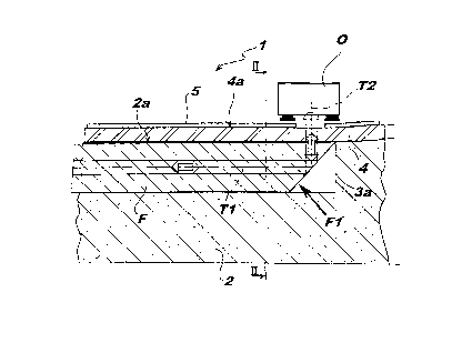
In the drawings, reference number 1 shows as a whole the so called optical
bench or
microbench SiOB (Silicon Optical Bench). It is in general a device designed to
allow the optical
coupling between one or more optical fibres F and a corresponding set of opto-
electronic devices
O.
1


CA 02299820 2000-03-02
As already mentioned in the introduction of this description, the device 1 is
capable of
being used both in the transmitter and in the receiving module of an optical
fibre link.
In the first case (to which - purely by way of example - a more detailed
reference will be
made in the sequel), the component O is formed by an optical source such as,
for instance, a
vertical cavity surface emitting laser, VCSEL, driven by means of respective
electric input signals
to originate respective optical output signals, injected into the fibres F.
In the latter case, instead, the component O is an electro-optic converter and
can then
comprise, for instance, an array of photodiodes or phototransistors designed
to convert the optical
signals arriving on the fibres F into outgoing electric signals.
In the attached drawings, the device 1 is depicted as a portion of a set
capable of
allowing - according to a general modularity diagram - the coupling of any
number of fibres F.
Even if the example shown in the previous drawings envisages the presence of
two
fibres F, this choice may in no way be regarded as binding. The number of
fibres F, i.e. the
number of the channels of the device 1, may be any. As a reference, the
experiments carried out
so far by the applicant have involved devices 1 capable of being used for the
implementation of
the following receivers/transmitters groups:
a single channel receiver with an InGaAs detector on both multimode and
singlemode fibres,
- a 10 - channel receiver with an array of InGaAs detectors on multifibre
cables
of both single mode and multimode fibres,
- a 10 - channel receiver with an array of InGaAs detectors with responsivity
optimised in the first window with multimode multifibre cables, and
- a 10- channel transmitter with an array of vertical cavity surface emission
lasers (VCSEL) on multimode multifibre cables.
Both the fibres and the opto-electronic components mentioned here are of well-
known
type, commonly available on the market. The nature and the features of such
components are not
however significant for understanding this invention, which makes it
unnecessary to provide here a
further detailed description.
Equally known (in particular from the article mentioned in the introductory
part of this
description) is the general criterion adopted to allow the coupling (both at
the transmission and
reception of the optical signal) between the fibre F and the components O.
In particular it is provided that the or any fibre F is subjected, along the
end to be coupled
to the device 1, to a cutting operation at 45° with respect to the main
longitudinal axis, followed by
an operation of lapping and aluminium deposition (or similar processes)
designed to originate an
end face F1 tilted in such a way as to reflect (and deflect) the optical
radiation.
For instance, the radiation travelling through the fibre (from left to right,
making reference
to the observation point of figure 1 ) along the path T1 identified by the
main longitudinal axis of the
fibre F reflects on the face F1 and comes out from the fibre along the
propagation path T2, which
is orthogonal with respect to the path T1. All this also involves the
possibility of arranging the
component O (here acting as a receiver) in alignment with the path T2.
2


CA 02299820 2000-03-02
In a dual way (in the operation as a transmitter), the optical radiation
outgoing (vertically
and from the top towards the bottom making reference to the observation point
of Figure 1 ) from
the component O along path T2 reflects on the face F1, so as to be deflected
by 90° and to
propagate in the fibre F along the path T1.
In the exemplary embodiment depicted here, the device 1 according to the
invention is
essentially formed by a silicon substrate of the same thickness, for instance
400 Vim, designed to
act as the support for the common mounting of the fibres F and the components
O.
In the substrate 2 in adjacency to one of the two faces (the upper outside
face indicated
by 2a with reference to the attached drawings) one or more grooves 3 are
obtained, each of them
is designed to accommodate in its inside a respective fibre F with an adequate
accuracy (i.e. in a
tight condition).
Each of the grooves 3 preferably exhibits a square cross section with a depth
of about
126 um, which has been machined with a high accuracy (tolerances of ~1 pm also
horizontally).
These grooves can be fabricated following accurate profiles with vertical
sides through
plasma ion etching. The relating technology as well as the _specific
modalities for making the
grooves 3 are well known in the technique and do not require to be described
in detail in this
context. It is usually a sequence of operations which comprises the
application of a photoresist
mask, the exposure of the same through a photolithographic technique, the
selective removal of
the photoresist parts corresponding to the etching zones, the ion beam etching
of the zones left
uncovered by the photoresist and the removal of the photoresist residual.
It must however be stressed that the above cited dimension values are purely
indicative,
since in other exemplary embodiments carried out by the Applicant, grooves 3
have been
fabricated (for instance 10 in number) with sides of 125 +1/0 Vim,
reciprocally parallel, with a
constant separation pitch, equal to 250 pm, according to the industrial
standards relating to the
fibre ribbons and to the arrays of emitters or detectors.
Reference number 4 indicates a glass coating (typically silicon glass, i.e. Si
O 2) applied
on face 2d of the substrate 2 as a cover of the grooves 3. The layer 4 is
preferably connected
through anodic soldering and thinned to a thickness which advantageously is of
the order of 100
~m or less.
The glass layer acts in practice as a cover for the groove or grooves 3. Each
groove 3
defines in this way a channel capable of receiving at its inside a respective
fibre F in a condition of
high alignment accuracy. This is provided in the longitudinal direction with
respect to the groove 3
(in particular concerning the positioning of the upper part of the face F1 of
the fibre meeting the
end wall 3a of the groove) as well as in the orientation of the fibre around
its longitudinal axis: said
orientation, in the event of more fibres connected in a ribbon cable, being
assured with a high
accuracy, in a practically automatic manner, just as a result of the
simultaneous execution of the
cutting and lapping operation, destined to form the previously described face
F1.
The glass layer 4 also forms, with its outside face 4a, opposite to the face
2a, a flat and
smooth surface, without surface roughness, which allows the mounting of the
components O in the
desired alignment condition.
3


CA 02299820 2000-03-02
In particular, the flatness of the external face 4a of the glass layer 4
allows creating on
the same the areas 5 (and the relating connections) which allow the mounting
of the components
O, in particular by a technique called reflow welding (also commonly called
"flip-chip bonding").
This technique allows, among other things, the fabrication of complete
circuits, suitable for the
hybrid mounting on the optical modules.
In the presence of more fibres F, the component O is usually formed by an
array of
individual opto-electronic devices, each of them being aligned with a
respective groove 3, so as to
be coupled to a respective fibre F.
According to a solution not illustrated in the attached drawings, but well
known to the
man of the art,
the substrate 2 and the glass layer 4 that covers it, may be extended also
beyond the
zone involved by the development of the grooves 3, so as to create surface
areas for the
implementation (in particular according to the standard manufacturing
techniques of hybrid
circuits) of the electrical signal driving/processing units associated to the
components 0. All this is
conducive to the obvious relating advantages in terms of general integration
with the device 1.
The glass 4 is obviously selected (through a choice which, at least in the
majority of its
applications, does not appear to be critical) in such a way as to exhibit a
high transparency degree
with respect to the radiation transmitted between the fibre F and the
components O.
While the principle of the invention remains unchanged, the construction
details and the
embodiments may be widely varied with respect to what is described and
illustrated herein, without
thereby departing from the scope of the present invention.
This holds true in particular but not exclusively for the coupling between the
fibres) F
and the components) O, a deflection mechanism of the optical radiation
according to different
angles with respect to the 45/90° angles to which reference has been
made in the previous
description (for example, a total reflection mechanism).
4

Dessin représentatif
Une figure unique qui représente un dessin illustrant l'invention.
États administratifs

Pour une meilleure compréhension de l'état de la demande ou brevet qui figure sur cette page, la rubrique Mise en garde , et les descriptions de Brevet , États administratifs , Taxes périodiques et Historique des paiements devraient être consultées.

États administratifs

Titre Date
Date de délivrance prévu 2003-08-26
(22) Dépôt 2000-03-02
Requête d'examen 2000-03-02
(41) Mise à la disponibilité du public 2000-09-03
(45) Délivré 2003-08-26
Réputé périmé 2006-03-02

Historique d'abandonnement

Il n'y a pas d'historique d'abandonnement

Historique des paiements

Type de taxes Anniversaire Échéance Montant payé Date payée
Requête d'examen 400,00 $ 2000-03-02
Enregistrement de documents 100,00 $ 2000-03-02
Le dépôt d'une demande de brevet 300,00 $ 2000-03-02
Enregistrement de documents 50,00 $ 2001-02-12
Taxe de maintien en état - Demande - nouvelle loi 2 2002-03-04 100,00 $ 2002-02-19
Taxe de maintien en état - Demande - nouvelle loi 3 2003-03-03 100,00 $ 2003-02-20
Taxe finale 300,00 $ 2003-06-04
Taxe de maintien en état - brevet - nouvelle loi 4 2004-03-02 100,00 $ 2004-02-20
Titulaires au dossier

Les titulaires actuels et antérieures au dossier sont affichés en ordre alphabétique.

Titulaires actuels au dossier
AGILENT TECHNOLOGIES, INC.
Titulaires antérieures au dossier
DELPIANO, FRANCO
OTC - OPTICAL TECHNOLOGIES CENTER S.R.L.
PESANDO, LUCA
Les propriétaires antérieurs qui ne figurent pas dans la liste des « Propriétaires au dossier » apparaîtront dans d'autres documents au dossier.
Documents

Pour visionner les fichiers sélectionnés, entrer le code reCAPTCHA :


Pour visualiser une image, cliquer sur un lien dans la colonne description du document. Pour télécharger l'image (les images), cliquer l'une ou plusieurs cases à cocher dans la première colonne et ensuite cliquer sur le bouton "Télécharger sélection en format PDF (archive Zip)" ou le bouton "Télécharger sélection (en un fichier PDF fusionné)".

Liste des documents de brevet publiés et non publiés sur la BDBC .

Si vous avez des difficultés à accéder au contenu, veuillez communiquer avec le Centre de services à la clientèle au 1-866-997-1936, ou envoyer un courriel au Centre de service à la clientèle de l'OPIC.


Description du
Document 
Date
(yyyy-mm-dd) 
Nombre de pages   Taille de l'image (Ko) 
Dessins représentatifs 2000-08-31 1 11
Revendications 2003-02-21 5 221
Page couverture 2003-07-23 1 44
Abrégé 2000-03-02 1 27
Description 2000-03-02 4 230
Dessins 2000-03-02 1 27
Revendications 2000-03-02 6 210
Page couverture 2000-08-31 1 44
Poursuite-Amendment 2002-08-21 2 69
Cession 2001-02-12 6 198
Taxes 2003-02-20 1 32
Poursuite-Amendment 2003-02-21 7 286
Correspondance 2003-06-04 1 37
Taxes 2002-02-19 1 34
Cession 2000-03-02 5 159