Note : Les descriptions sont présentées dans la langue officielle dans laquelle elles ont été soumises.
CA 02302015 2000-02-25
A read-only memory and read-only memory device
The present invention concerns an electrically addressable, non-volatile
read-only memory, comprising an electrically addressable non-volatile
read-only memory, comprising a plurality of memory cells which in a write
operation comprising a part of the manufacturing process of the read-only
memory, permanently each are assigned one of two or more logic states
according to a determined protocol which in the memory defines permanently
written or stored data, and a passive matrix of electrical conductors for the
addressing, wherein the passive electrical conductor matrix comprises a first
and a second electrode structure in respective mutually spaced apart and
parallel planes and with parallel electrodes in each plane and provided such
that the electrodes form a substantially orthogonal x,y matrix wherein the
electrodes in the first electrode structure comprise the columns of the matrix
or x electrodes and the electrodes in the second electrode structure comprise
the rows of the matrix or y electrodes, wherein at least a portion of the
volume between the intersection of an x electrode and a y electrode defines a
memory cell in the read-only memory, wherein the mutually overlapping
portions of the x electrode and the y electrode in the memory cell, each
defines a contact area in the memory cell, wherein at least one semiconductor
material is provided between the electrode structures and with rectifying
properties in relation to a selected electrical conducting electrode material,
and an electrical isolating material, wherein the semiconductor material in
electrical contact with an electrode in the memory cell forms a diode junction
in the interface between semiconductor material and electrode material,
wherein a first logic state of a memory cell in the read-only memory is
formed by an active portion of the semiconductor material covering the
whole contact area in the memory cell, the diode junction comprising the
whole contact area of the memory cell, wherein a second logic state in a
selected memory cell in the read-only memory is formed by at least one
electrode structure in the memory cell being covered by the isolating
material, and wherein a logic state in each case is given by the impedance
value of the memory cell, said impedance value substantially being given by
one or more of the following factors: the impedance characteristics of the
semiconductor material, the impedance characteristics of the isolating
material, and the impedance characteristic of the diode junction
t~MEN~E~ SH~~I
CA 02302015 2000-02-25 ,
.~ ~ o
n
a . ~n
~ .~
The invention also concerns a read-only memory device which comprises one
or more read-only memories according to the invention, and a read-only
memory device which comprises two or more read-only memories according
to the invention.
Matrix addressing of data storage locations or bit spots on a plane is a
simple
and efficient way of achieving a great number of accessible memory
locations with a moderate number of electrical addressing lines. In a square
x,y matrix with n lines respectively both in the x direction and the y
direction
the number of memory locations scales as n2. In one form or another this
basic principle is at present implemented in a large number of different
embodiments of solid state memory means. In these the memory location
comprises a simple electronic circuits which communicates to the outside via
the intersection in the matrix and a memory element, typically a charge
storage device. Even if such means have been technically and commercially
very successful, they have a number of disadvantages, and particularly each
memory location has a complex architecture which leads to increased costs
and reduced data storage density. In the large subclass of so-called volatile
memory means the circuits must constantly sustain a current supply with
accompanying heating and consumption of electric power in order to
maintain the stored information. On the other hand non-volatile means avoid
this problem, but with the trade-off of a reduced access and switching time as
well as increased consumption and high complexity.
Prior art provides a number of examples of semiconductor-based read-only
memories with electrical addressing in passive matrix. Thus US patent No.
4 099 260 (Lynes & al.) discloses a semiconductor-based read-only memory
(ROM) made as a large scale integrated device wherein self isolating bit line
surface areas of one conduction type are formed in a semiconductor substrate
and directly in a bulk area in the opposite conduction type. Channel stop
areas of the same conduction type as the bulk area are formed in the intervals
between the bit line areas. Metallic word lines which lie above and are
orthogonal to the bit line areas, are formed separately from these by means of
an isolating layer. The memory cell comprises a single Schottky diode. A
diode of this kind will be formed or not at each intersection between a word
line and a bit line depending on whether or not an opening is formed in the
isolating layer during manufacturing in order to permit the word line to
AMENDED SHEET
CA 02302015 2000-02-25, ~~ .,
w - ~' ,
_ . ., , ,
3
contact a lightly doped portion of the bit line. A ROM of this kind is stated
to
have a small area, high speed, low power dissipation and low cost.
Further there are from US patent No. 4 000 713 (Bauge & Mollier) known a
device with semiconductor elements, such as Schottky diodes and transistors
integrated in the form of a matrix on chips. The matrix may be custom
designed in order to provide a desired function. For instance it may be used
as AND or OR matrices in programmable logic arrays (PLA) or as read-only
memories which are stated to have better properties with regard to storage
density and power dissipation. A first electrode structure with parallel metal
electrodes of somewhat different design is provided on a semiconductor
substrate of for instance the p type. An oxide layer is provided on a
semiconductor substrate and openings are formed in the oxide layer to
provide anode contacts and cathode contacts via metallic lines which
constitute a first metal level in the electrode matrix. Two n+ areas are
located
under the cathode contacts. These areas extend to underlying collector layers
such that a Schottky diode is formed. Above the first metal level or electrode
level an isolating layer is provided and over this a second metal level which
comprises for instance an orthogonal second electrode structure. Openings
through the isolating layer ensure contact with a cathode contact in a group
of such which are included in the separate element in the matrix.
Finally there are from US patent no. 5 272 370 (French) known a thin-film
ROM device based on a matrix of open and closed memory cells formed in a
stack of thin films on glass or another substrate. Each closed memory cell
comprises a thin-film diode and it may by using stacks of semiconductor
films, for instance of hydrogenated amorphous silicon, wherein the separate
films are of different conduction types, be obtained diodes with different
conduction characteristics. Thereby the information content in the ROM
matrix may be increased. Each memory element which is formed with diode
structure, may then be set with different logic levels according to some
manufacturing protocol. Where the memory element does not have a diode
structure or where the semiconductors are covered by an isolating layer such
that no electrode contact is formed, the memory element may be used to form
a determined first logic level, for instance logical 0.
Even though the above-mentioned prior-art devices all realize electrical
addressing in passive matrix in an as per se known manner by providing
AMENDED SHEET'
CA 02302015 2003-07-18
<~
diode junctions in closed electrode c~ont.acts, they have
partly due to using different types <>f semiconductors a
relatively high degree of comp:~exity. Try true PROM device
as disclosed .in thEa last-me~nt~:ir3ned p~.l.blication (LJS
patent ~ 272 3701 it may, however, b~~: possible to store
more than two logical values irn the matrix, but th.s
presupposes use of diffee~er~t diode t:~~°pes and hence
several layers of differentl,r doped sc:~mi.canc3ucwtors in
the bit spot with diode jun.~.~_t:ic>n.
The object of the present: invention is hence
primarily to provide a read-only rnemc>ry ox F20M which
permits electrical addressWng irs pas~~,i.ve matrix to the
separate. memory cell in t:he :ro~Kad-oz~l~,~ memory and wY~ich
does not need refreshment in order tc.~ keep the data
stored in the memory cell, while the ~e°ead-only memt>ry
shal l be s imply and cheaply x~e;~.:L ~ zerl us irrg as per ~;e
known technologies and methrads <~s applied. :in they
semiconductor and thin-film technoi.ogy.
Particularly it is the object c~f the present
invention to provide a non-v:r~~:l.at.-i.l~.~ zead-only memoz°y
based on the uses o:r organic rrrat:e~c~ial~, for instance
polymer materials, which .rea.l.~..xed :a.n thin-film
technology may be used both in conductors, isolators
and semiconductor materia.l.s, somet.hin~~ which supposedly
shall provide more :Elexi.ble technical s(a Lut.ions and.
especially a much x.-educed cost. than. would be the case
when using crystalline inorganic semiconductors.
Further it is also are c:k.~jer.t: to pro~r ide a
read-only memory which al. lows a rnu~.t:.:~..:le~~rf~l c.odin.g of
predetermined memory cel ~ s or memory Ioc~:~t ions .
Finally it is the object of. the present invention
to provide a read-only memo~~,~J which may be used to
realize a volume~trir_ rea~~-only memory de~,ri.ce.
CA 02302015 2003-07-18
These and other objects and advantages are
achieved according to the a.:mrent i o:n uvitka. a read-onay
memory which is characterised :in that one or ano.re
additional logic states in a memory c~~e11 in the re<~d-
only memory is formed by tree acxtive ~5c:ar~t: ion of the
semiconductor material covering only a part of the
contact area and that the d:ic:ade junct.i<:~n. only compwises
a part of the contact area, sz.z.r.h that: the data whi<:h
are stored in the memory may be repx-~~~sented by the
Logic states in a mufti-valzaed codes arzC~. that said one
or more additional lagic states are given by impedance
values determined by extNn:,i.orz o~ tk~u~ active portic:5n of
the semiconductor. material and an extension of the part
of the contact area which forms the ~.iode .,junction.
A first read-only memory c9eva.c~e accr,~rding t.o the
invention is characterized in that the read-only memory
is provided on a swbstrate ~~~f semic:;;oracluctor material
and via the substrates connected wit=h driver and
control circuits fc~r driving a:rnd add r:essing, said
driving and conr_x.°o7 ci.r<~ui.t. being ir:4tegrated in trze
substrate and realized in a semiconductor technology
compatible with t: he subs~~rat;c_. rnat:e:r. a ~ Z ; ar~c~ a se~cor~d
read-only memory device according t.o the invention is
characterized in that tkxe rt~aci- oczly memory :is st:ack:ed
in horizontal layers i.n order to provzde a volumetric
memory device, that the volumetric rztenzary device is
provided on a substrate of :~erc5i<.pnc~.uc:tor material and
via the substrate or the substrates connected with
driver and control cir~:ua.t:s f'caa.° c~riv~.ng sand addressing,
said driving and control circz.zits being integrated with
the substrate and realized irr a senzic~onductor
technology compatible with l::kie ~aub~str<~te rrmteria.l.
CA 02302015 2003-07-18
Wherein the read-only m~:mcxy ac:cvc~xcling to the
invention is real.i.zed as abinary l:ag:i.c° memary, i~~ i_s
advantageous that the first: logic state which either
represents a logical C' or' a Io<:~ica;l ;.., ~s given by the
effective forward bias res:i.s t:ar~c~e of a diode formed i.n
a memory cell wherein the semicanductor material
contacts both the ~ e:l.ectrc:~dE= anal ti~~:e y electrode, and
that a second or additional locyic st.<.ste:- which
correspondingly represents either a a.ogical 1 or a
logical 0 is gl.VFPT1 by a ~e7.ec;thad r.~e>:~.stance value :far
the isolating mat:eria:l prov:ide~~ in a memory cell.
wherein the semiconducting material at most contact:.s
either the x electrode or the y electrode, said
isolating material in ~~ mernax-y ce.l:l ~:~refexvably having
1S an infinite resistance value.
Wherein the read-only memory according to the
invention is realized as a mu:l.t:ilew~:7.. logic: memory with
one or more additional logic st<_ates, it is advantageous
that the first logic state is given by the effective
forward bias resistance: c~f a ~l:i.~ade t:carmed :in ~a memcyry
~_elI wherein the semiconductor material contacts both
the x and y electrodes and that. the additional logic:
states are given by determiner( resistance value: fc;r
the isolating mate:~~ial provided :~n a memory cell.
wherein the semiconductor material at most contact's
either the x elec°trade ox- tEze ~,= a:Leo°t:~~ode and the
selected determined resistance value in each case lies
between the effective forward bias resistance of a
memory cel:L forrnE:d .in thee di.ade., anc~ inf i.nite.
In a first embodiment. of; they read-amly memory
according to the invention the isolating material in
:elected memory cel.Is i:~ pro~,rided x»~twee:l t:he electrode
structures in the farm ai: a ,~~rparat.e l.ayer~-like
CA 02302015 2003-07-18
'7
isolator patch whi.c:h wha:l.l~y or' ;~~art:l~~ covers at le<~st~
one of the electrodes in t:xc: merorary cea:a., a selected
memory cell dependent on the active portion of the
semiconductor material arid the diode junction part of
the contact area i.n the lat:.:t.er case acqt~uiring a logic
state which corresponds to a l..cevel. or a m~.zlt:i-value-~d
code.
If the isolator patch in said first embodiment
wholly or partly covers only one of the electrodes, the
semiconductor material may be provided between the
electrode structures i.n ~ c~~..c:~b<~1 ~..~y~~e and besides over
the isolator patch in the sel.ect.ed m~:emc-~ry cells . I:~ the
isolator patch wholly or partly covers both electrodes,
the semieonducto:r material may prefex:°ably be provided
between the electrode struc~:ures and adjacent tea the
isolator patches in tree se:l.ected memc:~x-y cells, sucl,~
that semiconductor material and. the= :i..sol4~tor patc=hes
mutually flush in a common continuou:x layer.
In a second embodiment of the read-only memor~~
according to the invention t~ze :isolut:::i.ng material :'~s
provided between the Plec~trode st::ruc~t:.ures in t=he farm.
of a substantially global. l~ve:.r~ whiciwc cc}vers <:~t least
one of the electrode structures and with removed
portions in selected memory cells, such that removexd
portion wholly or partly exposes the: elect.rodes in a
selected memory c:e~_1, said ncemc:~x-y c~e::l.l dependent: on the
active portion of the semicondl.zctox~ material. and/or the
diode junction part of the contact area in the latter
case acquiring a logic state which corresponds to a
level in a mult.i-volued ~:od.t~.
If the iso-aat:ing Layer in said second embodiment
covers only one of the e3.ectxvode st:ru~cture;~, the
semiconductor material may preferably be provided
CA 02302015 2003-07-18
fl
between the electrode structures and over the isolating
layer in a global layer anc~ be=sides c:ont.act. the
electrade structures in the removed ~aartions of the
isolation layer. If the isolating layer covers both the
S electrade structures, the ;,~:~ni~:~c>ndu~:~i~,Jx- material m:;ty
preferably be provided enl;r between ~_.he electrode
structures and adjacent to the i.so:la~~-ion :Layer in the
selected memory cells, such that. the.=, semiconductor
material and the isolating Layer mutually flush in a
common continuous layer. Finally, it is af~cording t~.o
the invention advantageous ~kzat~: t:rz.e ;>emiconduc~tor
material is amorphous siliaan, palyc~.x-ystalline sil:i..con
or an organic semicanductox, said arc~arzic semiconductor
preferably being a conjugat:ec~ pc~l.ym~a~ .
According to the inventi.an the semiconductor
material may be an anisotrapic: e.:~nduc~tor. Preferab:Ly
the semiconductor material may c~~mpx~:i.se more than rune
semiconductor or possibly also be added or combined
with an electrical canducting ma~~e:ri.c~l.
Preferably t: he semi<,orz~.~u~t:o:~_ nzvt ex°ia.l, the
isolating material and the electrode structures are
realized as thin films.
The memory devices according t:.c~ the inventi.an
advantageously comprises ar~ additional substrate
covering the respective rauemory dev:LCw; oppr~site a first
substrate and p:roVided with fur~<:t.iarc.; similar to trzose
of the latter
The background of the inventian and various
examples of its embodiment szza~..l nc:~w~ xae discussed in
more detail in the following with the reference to the
accompanying dr<~wirzg .
CA 02302015 2003-07-18
9
Fig. 1 shows schematically a general embodiment of
a memory device with a passive electrode matrix
provided between backplanes c.~r subA~t:::r:-at.c-;s,
Fig. 2 schematic examples of sneak current loops
which rnay arise ::in a matrix, c>f this 3~~.ir~.c~.,
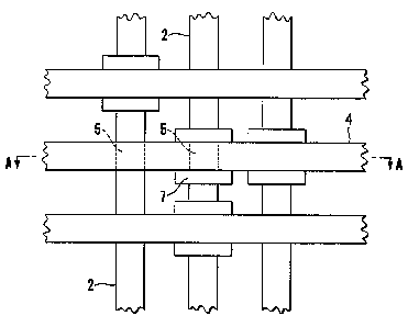
Fig. 3a a first embodiment of a read-only memory
according to the invention and seen a.n plan view,
Fig. 3b a section through ttxe read-oxzly memory in
Fig. 3a taken along the lix:m A-W i.r:1 a. ffirst variant: of
1U this embodiment,
Fig. 3c a sect: ion tlrro~.agh the read-only merriory° i:n
Fig. 3a taken along the line A~-A in a. second variant of
this embodiment,
Fig. 4a a second embodiment of the read-only
memory according two the nvent:i.c~n :peen in plarx view,
Fig. 9b a seet:ion t:r:rrougY~, t:.Y~e xe,:~d-~:ml.y memory in
Fig. 4a taken along the line A~A in a f_i.rst variant of
this embodiment,
Fig. 4c a section througYr the read-only memory in
Fig. 4a taken along the line P,-A iri a second i~ariar..t of
this embodiment
Fig. 5a an example of rnult:i.:~.evel c:ociing of a
memory cell in the embodiment in Fig. 3a,
Fig. 5b a section through the memory cell in Fig.
5a taken along the line B-B,
Fig. Eaa an example of multi.eue~.1 ~.orai..ng of a
memory cell in t: he embod~.me.rut: in Fig. ~~a,
Fig. 6b a section throv:~c~tu t:he rn.ei~raorwr~ cell in Fi.g.
6a taken along the line E~-B,,
Fig. 7 a sectional view through ,~ f:irst read-only
memory device according to the ixxvenC:ion, and
Fig. 8 a sectional vie~b~ thrvough r::~ secoxad read-~.mLy
memory device accm:~c3ing to t: he i.x~.vent:a..on,
CA 02302015 2003-07-18
The general background of the i~aweration shall now
be discussed me>re closel~P. 1'-~ genex°i~u ma;:x-i.x addressing
system is shown in Fig. I, whez:ein for ::i.nstance m
electrical conducting lizle~ ~ ~.i:~e rc~u~~ua:Lly spaced
5 apart and extend i.n a x disc-ec:t:ion aa:~:i w:i.t:h for instance
n overlying electrical lines 4 which ex~~end in a y
direction and respectively form 1=irst~ arid second
electrode st.ructm:es in an ox~t:rioganal x, y electrode?
matrix. The x electrodes 2 and the y electrodes 4 .are
10 provided sufficiently closes t.a a<~cl~~ ~_.~thc:.x such that
geometrically well.-defined ~:we:~-lapp:ir~g ~:mea.s or
intersections between the electrodes are provided. The
volume near and between eac:~t-i i:nterse~~tic>n, coarsel,~r
defined by the ove:x~lapping area whi~:~a.r is; c~i.ven :by ~t:he~
IS width of the intersecting x electrodes and the y
electrodes in these ir~tersectic:~rm, :ornprises what in
the following will be denot:ec:~ ~a.s a mt..~mc~ory cell 'S, ;:~ee~
Fig. 2. The mutually overlapping areas of respecti~Vely
the x and the y electrodes '.~ ~ 4 , in a rnenuory cell ~ will
be denoted as the contact areK~ of tlm~ mF°mory cell.
According to the invention data i.s st.ored in each
memory cell as impedance values, far instance
resistance values k~etween t: he a<.. .and i:lie y electrode. in
each intersection. The logic state :~.r~ each intersec.:tion
or memory location is found by measurine~ electrical
impedance between the x elect:t..-c:oc.~~~ ;:xr-rc:l. tree y e:Lectrode
which intersect each other in tha memory ~:.,e11.
Distinct from common kLrcwrr cur rent-addressed and
matrix-based memory systems; the ,prevent i.nvent:ion
allows the use of a purely passive electr:i.ca7.
addressing, as there are no discrete active circuit:
elements in the memory cells. it is Well--kruown t: hat: the
use of electronic. memories with memory cells in pa:~sive
CA 02302015 2003-07-18
11
matrix is encumbered wit.lu ,~lt~erz~at:i.v~= caarx~ent paths or
sneak current paths in the electrode matrix. This
problem is indicated in Fi~y. ? whex-e a:it.ernative
current paths generated. by add.rE2ssi.n~1 t:~le memory ce:l1
5k1 given by the intersection between: the electrodes mK,
n1 are indicated by tlninnex st:. i.t~:heca :l:iraes to the
neighbouring memory cells. When. the ~i.zF: of the matrix,
i.e. the product x~y increases, then t:he sneak current
problem also am~pli f ies . :ff the memoryr e.7.ements in each
intersection has a purely resistive impedance this
implicates that the resistance difference in a write
operation will be masl<:ed b;r ~::w:K~xwntA~ wl::~:i eh leak through
alternative current paths, such as indic.sated in Fig. 2.
If the electrical connectic:~xa i.za each :Lr:~t:ersection ~s
given a highly nonrylir~ear c:uxrrent-vca~..tage
characteristic, the sneak current problem may be
reduced or wholly eliminate=d, ~,~nu:ite ,~~in~~?ly this is
achieved in a mann~:r which ig already well-known and
suggested in the art, rrarnel.y by pro,a:iding a rectifying
diode in series with t.rxe i.mpE~d~~.zice ~>:c~ x:esistance irz.
each intersection.
An essential !foal of the present::: invention i.s
forming a network of di.ode> «f this lr:-ind in a m<~nnf=r
which simple, cheap, reliable and which simultaneously
allows the use of suita:bl.e rosemary st:x~uc~tux:es in they
form of controllable impeda:nces_ A.c:cord.ing to the
present inventioir the x arzd. t.lre y electrodes may
preferably surround a layex caf :aerra:ic.;c::mnd~:zcting mat:ez~ial,
for instance in thin-film confa_guration. Particula~__°ly
this semiconducting materi.a.? ~n4:~y aci~r~~.rztageous::i_y be a
conjugated polymer of the tiopr:er~e c~z- PFV-type. ~y
choosing a suitable electrode mate.r:ial with regard to
the semi conducting material, a diodes _juncti.on is
CA 02302015 2003-07-18
L2
obtained at the electrode-:~emi.c::r_snductor int:erfa.ce and
the diode may be given very good rectifying properties.
A simple linearized analys~.~ shows tUzat the number of
electrode intersections, i.e. memory ce-Lls which may be
addressed without distox tioru or_- z-:oise d~.ie to sneak
currents, is appx~oximatc:ly equal to 7::he diode
rectification ratio in each intersection, i.e. the
relation between forward and backwards i:lowing current
at a given bias vc>ltac~c .
Another basic prablem with passive matrix memories
as exemplified in Fig. 1 wliexe~.n t~ze corat::inuous
material layer with finite resistance: a:~øtends in t2ne
intervals between the intersecl.ions .~f the electrode
matrix, is that currents a;~~en wit:h pc~rfecr_
rectification in each intez~secti.on rnay flow betweexn the
electrode lines 2, 4 in these :intervals. Even if the
path length in these intert.~a.ls will lie nkuch longer than
which i.s the case in the intersections, i.e. in the
memory cell, and the layer between tine c;lectrode
structures are extremely t,x~ir~ wi.t:h tra_grr surface
resistance, the combined effect. of many such current
paths is detrimental t:o the measured i~ry~,edance and
hence finally sets an upper. l..imi.t to thE: number of
intersections and so also c:f menrorwy cells which may be
realized in a passive matra.x..
The last kind of crosstalk may be avoided by
making the film conductance highly amisatropic, i.e.
with high conductance irz t:he desired c~uxrent cii:~eci::ion
and else low conductance. In case of- Fig. 1 this w:i..ll
correspond to hic~tl condizc~tavr~r~ perpc~r:~dicu~.arly to i~he
plane of the matrix and 1. ow c~cand.uc.taz:~r.~e in the mat.x°i.x
plane. Polymer compositions with. properties of this
kind have been described in the lir_e:r_~at.ure, for
CA 02302015 2003-07-18
13
instance in the paper "Whit:e light err~i.ssion from a
polymer' blend light emitting diode" caf M. Granstrom a.nd
o. Inganas, Applied Physics Letters ~B, 2:147--149
(1996) , and e:lect~rode means anc~ devices based thereon
have been disclosed in NO pat:ex~t app:iication No. 9'3390
which has been assigned t.o twhe p:resern.t: applicant.
Starting with an as per se known, basic structure
as shown in Fig. 1 wherein the x and y electrodes ~?;4
are provided on each side of ,:xxv ani:~catrapic thin f i lm
with high rectifxc~,~tiorz r~ati.c> in t)m:, zx~ter5ect.ions of
t:he electrodes, data may be c:roc~ed )air a coxzt~roa_lE.d
deposition of an electrical isolating material between
diodes in selected intersections, such this will be'
discussed in more detail in corxnection with Fig. 3a. If
such selected intersect.ians ar~e~ ~~iver:~ an anfir~it:e
resistance, each i~~tersecti.c~r <~.~:r.- eac:Ya. memory cel.1 can
be binary coded, for instance with a. forward bias
voltage which either gives logical 1 as R = RF., where RF
is the effective forwards bras :eesist~ance of the diode
in this intersect ion, o:t:- 1o~~3ic: 0 a;:a R =- ~~ , where an
:i.nfinite resistancE: on purpc:>se have been inserted in
the intersection. F-i.ighc-r data .~,1-c,x-ac~e capacity will be
obtained by using a larger range o.f resistance values,
which is equivalent to several bits being stored in
each memory cell, f:or instaxrce with resistance values
R.z, R2, R3,..., RF < Ra < R~ <~ ~~ <
A first embodiment of t:: he re:~ad--farxly memory
according to the ir~ventzon ~~ha,ll. now be caescribed with
reference to Fig. 3a-3c. 7n this case the; a.s per se
known the generic structure as shown in the figure -is
formed by deposi.tirig the. x electrodes at the bottom
substrate 1. (also shown i.ri :f~ic~. ~.) or b<~c:kplane which
CA 02302015 2003-07-18
I4
may be made of a semiconducting 2 mate vial. and
comprises active circuits far uic~r~al pr~c~:ssing,
routing and logic man:ip~alatvic;~rv :integrated with the x
electrodes 2 which here form a first electrode
structure in the electrode mat.r.~.~. C,~r:~f:~spandingly a
top substrate ~ (also showzr i.rr ~'ig. 7_) rnay integrate
circuits with the y electrodes 4 i.n the same manner and
for corresponding purposes . Tt slaal 1. be: understood that
the x electrodes ~; and the y electrodes ~ may be ~xsed
for forming for instance b.it lines and word lines in
the read-only memory accvorc:l:~.n.g t:c> tn=~ irmention. Bath
substrates 1 ; 3 with circuit s arid el.c=,~t.rc~des 2 ; 4 are
processed by means of standard semiconductor
technologies and i t may f a:~- :inst:.ar~cc= be used a
crystalline semiconductor wafer, for inst.a.n.ce of
silicon, as substrate . Alternativel;~, flue silicon ynay
consist of amorphous silicc:~n or sem::i.;~oru:luct:ing organic
materials on rigid or flexible supports (backplanes).
In a following step may now eiY~her tale c~f the
substrates 2 ; 4 or both 2 , 4 lie c.°aded c>tac:l tlZat t:he
resulting read-only memory receives the desired
information content . Advant:.~gec~~usly °:.lZ:i.> is d~~ne b''r'
providing localized isolatc~x~ or re:suatraz films ~6 izi the
form of patches 7 over the electrodes 2;4 on one of the
substrates 1; 3, such that tr:~ey wi 1l l:~e positioned :i.n
the intersection between or x elsct~-cade and a y
electrode. Materials which a:re common in the solid
state technology may be used anl. l.:ikc==w:i~e well-known
technologies for depositing and ady..mtment. Over tlne
isolator patches on the resistor pat:c~loes '7 a global
semiconductor layer ~ (also shown :ire F~ i.c~ . 1 ) is now for
instance deposited such as shown in ~'ig. 3.b (the
semiconductor layer 9 is for the sake of olarity
CA 02302015 2003-07-18
deleted from Fig. 3a), which simu:~.taneoczsly forms a
diode junction with the electrode material in ane of
the electrode ~~tructux:es, :f:cw a.r:~st:r~nce t:: he y electrodes
2. The chosen semxcanduct.oa: ~r~atcz~;ial anc~. the chosen
S material in the electrode ;~,r_xwct~.zrH may b~e such that
where the exposed portions of the elect ode structures
physically contact the sem:l.canducta:r mat:.erial,
rectifying junctions or dicade juncti.~rrs are
spontaneously formed.
10 The semiconductor material used must have suitable
rectifying and conducting pr opEZ_~ties Y whii.Le it is
desirable with law bu~.k c:o:t., s~.mpl~~ prc:>cPSS.ing, a long
lifetime etc. and must. be su.~h that opta.mal contact to
the material of the electrode structures is obtained.
15 As semiconductor mater ial rc~:~y f:or in;~t~:.~mce conjugated
polymers of either thF~ ~~?V or t_.hiog~~~F.:n~: families b~~
suitable. Alternati..vely amc:~rphc:n.~s s~_~..~cvc:~n or
polycrystalline silicon ma~° be used together with an
anisotropic conducting thirx film of ~alastic material.
The basic procedure of the msnufs.cr_u..re r:equirr~s a
precision adjustment when t;h~~ :isol<~tc:>:r patches '7 i:~a
deposited on the electrodes 2; 4. Thia step ma;~r,
however, easily be implemented with K~. di.rect exten:aion
of manufacturing processes f oz: act i~,rc:;:~ c:~ rc:n.zita witlu
electrode matrices. c.~~labal dc~pc~sitic:au~ of semicomduc:°tor
film 9 such as it is shown in Fig. 3b, may be perfczrm.ed
without any kind of precision adjustment. 'fhe y
electrode 4 must, however be pr~c~vid~~c;~ i.r~ such mannE:r
that the isolator: patches T are lac<at~ed irc the
intersections between the electrode structures. This
requires a higher positioning accuracy the closer the
intersections are provided. i:n that caiunectian the use
of a transparent tap substrate ~~ with. semiconduc:t:oz:
CA 02302015 2003-07-18
~b
circuits based on organic senuic::«rxcluc:.tor a or amorphous
silicon in combination wi.t.h thin film of semiconductor
polymer may offer possibilities for an adjustment which
cannot be achieved by using non-transparent substrates
of crystalline si_C..icon. I:n t~i~.e embod:ime~zt: in Fig. 3a
the resistance values of the a.solator patches 7 may be
varied by using different isolating materials, possibly
by varying tLae thickness o:r tlxe. form ot_ t:h.e isolat(.or
patches. It is hent:e very well possible to obtain f~.
multilevel. coding such that fox- instance the memory
cell ~ in an intersection wherein no isolator patch 7
has been provided, may repx:ese~at a l~.~g~.~a:L 0 while
further logical values may k~e ~ust.oreci ir1 rrvemory cel:)_s
wherein isolator patches with varying ge=ometry or made
of materials with different reaistanc.:e values are cased.
In a purely binary coding t: he l.mpedaa:~.ce values of ,:all.
isolator patches will <af cc:>u~sc~: be t_:ioe :~a.me. They may
then all be made with infinite resistance. A
particularly preferred method to obtain binary coding
in the embodiment shown in f:ig. 3a-;::: sh~~l1 also be
discussed below in connection with ~::i.g:~. 5a and 5b.. If
the isolator patches 7 have the same thickness, thr
semiconductor layer 9 may as shown ire fig. 3c be
provided between the e:Le~°tx.ocie:~ ~~, _~ such tha~.. they a.re
flush with the surface of the _solat:c.:~r patches 7 , 'This
may entail further advantages with regard to eliminate
and reduce stray currents and ;~tx°ay c:::apacitances. an
the variant embodiment i:n F':if~. 3t~ atu;°ay capacitanc:E.s
may arise or stray currents maZT flow to the
semiconductor bulk material ~. Tads may, however, be
eliminated by using an aznisatropi.c sernicorzdr_~ct~or_ a;a the
semiconductor mate:r.ial, the S::~oxvduct~..G::~r~ cli.:x~ect.zon oi=
which extends between the electrode structures. If,
CA 02302015 2003-07-18
1 '7
however, the semiconductor layer 9 is faush with the
surface of the isolator pat~c~h '~' as s~~awra ira Fig. 3c:,
which is expedient when the iso~.at.ar_ patches have the
same thickness, the distance 'between tam electrode
structures may be reduced Maraca r,;:he sem:icc:unductar :La:yer
generally be made much thinner, such that the
semiconductor material doer .not. mead to be anisotr.~~pi.c
conducting, while possible b~a.:lk c~urrent.~simultaneously
are strongly reduced. The dude junct~ior~ between tile
semiconductor material. and one of the: electrode
structures will, of course, simultaneously be
maintained and reduce or el.:i.rn:'tanate t:~~e danger for :sneak
currents via the electrode structures.
Fig. 4a and 4~b show respec:~t.ive.~i..~ in p:Lan view and
l~ in sect ion taken alone the l.:i.rm: A-A :~, rz E'.ig . ~a anat~her
embodiment of the read-only memory according to they
invention (the se~ma_conductor layer ~~ a~.so here deleted
from Fig. 4a). The electrode structures are as before
deposited on respective bottom a~zd t:c>~S substrates a.;3,
but an isolating layer 5 is, ~~.c~w depc~:~i.t.ed aver t:he
electrodes 2, 4 and between thre electn:rode structures
and over one of them as a subat,~z~t:ially global layer,
but with removed portions 8 i.n predetermined
intersections for t; he pu:e~pose ca.f. fcornoa.rxg therein memory
cells 5 which stare other logical v,:~.'~~es. A
semiconductor material 9 whickx now is deposited aver
the top of the i;so l ati.ng layer. f~ , ~~~rc~ Fig . fib, wil 1. of
course only contact both electrode structures in the
removed poxtions 8 or "w.~ndc~w;~" in tree i.sol.at~.ng layer
6, such that the memory c~ell.s 5 at these removed
portions for instance may store a binary logical value
~), while the memory cells 5 whe~re:ia°u c;n.e c~f t: he.
electrode structures is covered by the isolating layer
CA 02302015 2003-07-18
1.. ~3
6, stores a binary logical value 1. Similarly to the
embodiment shown. in Fig., 3a" a:lsa here i:he
semiconductor material 9 may be provided such that it
is flush with the isolat.inc:~ layer ~~, l . «;~ . i.t will an:ly
be located in the removed portions 8 or the windows
with the above-mentioned advantages result:i.ng
therefrom, such this is disclosed in Fig. ~c, where r_he
semiconductor material l s :aYzowzr as a "pat:ch" 10 over an
electrode 2. The manufaotu7:ing ~~t:.ep for the embodiment
in Fig. 4a-c may shortly be summed up as comprising
depositing of ~: elec:tx~acies ~:~n the substz:ate 1, applying
a substantial global isolating l.aye:r 6 c:~oded with
removed. portions 8 or wirzdc7ws az~.d t:;hF~re;~bave applying a
global semiconductor layer 9, while the y electrodes 4
is deposited on trie top sub:_ttrat~e :3, wt~.~:reafter the t: op
substrates 1,3 with deposir_ed eiectrode:~ 2, 4 isolating
layer 6 and semiconductor :La4~rer r~ a:ra=~ jcai.ned into a
sandwich structure. An advantage of the embodiment
shown in Fig. 4a-4b, ~s that t:hc> senn:icozzductor doer not
need to be an anisotropic semic:cmdu~rror,. while
simultaneously stray c:urrez-~t:s ;:~r~d sam~ak currents
outside the intersections between th.~~ e:l.ectrodes
substantially will be completely eliocvinated. Tn
addition sneak currents thz::.>ugY~ trze c:liorle functions are
reduced, as current only will flaw where a window is
located in the isa.lati..ng 1<a.y=e:r. ~ re r; t:r-..ction to t:he
use of binary coding only makes i.t pc~ss~.ble to increase
the data storage density b~,« rec;~~a.c:ing fi.h~::~ Lzorizonta:l.
distance between the electrodes in each electrode
structure, such that area clez~s:ity at: th~:~:, memory cea.l~:
increases. Typically the sneak current background will
be halved in a binary codirz~; scheme ~~r:it:.Yi. ozze :~za:l~ :zeros
and one half ones, and this wi.l1 al:l.c~w that the number
CA 02302015 2003-07-18
i~
of memory cells ar intersectian:~ i~:~. the electrode
matrix may be c3aubled with rn<~ir~t:enaxi.ee of t:he. same
basic signal-to-noise rat:ina :i.za the addre~asinc~
(reading). Also in the embodiment in Fig. ~a-c logical
values based on a multilewe~ code mar be stared, such
this wi_11 be explained more c~l~:~.:~ell~~ i.n t~h~.> following
with reference to figs. ~a rind ~~b
Figs. 5a and 5b show .ira pi. an view and in section a
memory cell in the embodiment of the read-only memory
as shown in Fig. 3a and 3c. 'I:'he isolator patch '7 which
codes the memory cell !a ~..s hex°e realizeca such. that ir_
isolates only a part c.7f the c:ontac:°t~ are~~ i.n each memory
cell, in contrast with the Pmbodiment shown in Fig. 3a,
where for instance the isolator patch T7 isolates the
whole contact area 1.1. ~?,s :k_>c-Mare the semiconductor
material 9 is provided between the e:lect:rades 2, 4
above the isolator patch 7 and ss before: a diode
junction is formed between one of the e<<ectrodes 2, 4
in the memory cell 5 and the secoiconduct~or material 9.
The diode junction may for ir~st:ance :i.n t:;he embodiment:
in Fig. 3b be identical wit:l-c tl~ze cc~n~:act: area 11, but:
if semiconductor layers 9 flush with the isolator
patches 7 are used, as in Fig. 3c, the area of the
diode junction will of course be reduced to that part
which i.s not covered by the: is~.~lat.or pat.;ch 7. The
effective conductor crass section and twlxe bulk
impedance in the semiconductor material will in thin
semiconductor layers or anisotropi.c semieonductor
layers depend on the effect: i~,~e cont~~r::t ~w.rea w:~ich i.n
figs. 5a, 5b is limited to t:lnar_ part of the electrode
2, 4 which is not covered by the iso:i.atar patch 7. This
effective contact area whic:~ may be different from the
area of the diode junction, detines a~n active portion
CA 02302015 2003-07-18
in the semiconductor between the electrodes 2, 4. By
using isolator pa t:ches of c:liffer..ent ~~i.ze:~ far codinc3 t:he
memory cells, i.t may ~i.n th::i ~; manner ;auir:ably be stored
data in a mufti value code.
5 A coding of tlxe memor~a cell.:; ~ :l.n the embodiment
in figs. 4a-~c takes p:l.a.ce ~.rl irmerse azralogy with the
method shown in. figs, 5a and 5b, as now it is, as Shawn
in Fig. 5a, the extension of the removed portions '~ or
windows in the isolating lG~yNx~ c3 whi~:.h cretermines t-:he:
10 effective contact area :in t::.t~e rcvemor~a c:el 5 a:nd if the
variant in Fig. 4c i.s used, also the diode junction
part of the contact area . 'fhe ;~emicanductar materi,~l 10
which is provided ovex° for instance r:he x. ele~.:t:rodt~ 2.
in the memory cell 5, hence has its bulk impedance
15 reduced substantially in correspondence with the
reduction in the effective co>nt:act s,~a::~ea arid by ~;rar~Ting
the size of the window 8 :in the isn~l~at:i.r.~c~ layer 6 :z.n
this manner and hence the effective contact area, data
may be stored in the memory cells w:i.t.h the use of a
20 mufti-valued code.
It shall here be remarked t-_hat. coding of data with
use of mufti-valued code places greater demand on
discrimination when reading t~.he impec:3.ance value in a
memory cell and i f there is a ~>reserit:: danger of bu7..k
and sneak currents masking the impedance value signal,
either the mutual ciistana a between tire electrodes 2, 4
in each electrode struct~.are az~~c~ henc:~> the memory ce~ll.s
5 may be increased or else the mufti.-valued code may be
employed with the embodiment variants shown in
respectively Fic~. 3c and FiG~. 4c, wl~:ich easily will
allow the memory c:e.lls t~:~ be lc~catec~ with a gx-eat. area
density and with maintenance of the discrimination
which will be necessary to obtain a readout of the data
CA 02302015 2003-07-18
~1
stored for instance in a two-bit; code, a. . a . with two
levels between the code le;~~~el shivers r>y i:;espectively a
complete masking c>f t:l2e cozwt:~ct: area in the memory cell
and a complete expc7sur~e of tat3e c~ant.a~:~t area in the
memory cell. It is, howeve7.~, s~.zpposed t.r~at it will be
possible to increase the number of :l.Nve7.s in the code,
for instance using three- or four-b.i.t coding. The
latter is represented by sixteen. levels and hence the
realization will be a quest:ia:n of dimensions and
achievable pitch if the manufacture ref the memory cells
takes place with convez~tior~sl. cnicra-~~:Shot:ol.ithographic
methods.
It may be e~:pedient to fi. or_ m tale ~~emi,::anduct:ar
material from several semicondz.zcto:r;:a, fc:r instance
provided in layers, such as kzrawn its the a2:t, in order
to obtain special types of da..cades, such. as also known
in the art, or in order to var~~ the impedance
characteristics. Far the same purpose also the
semiconductor material may be combined with or addE~d an
2U electrical conducting mate rial.
One or mare read-oznly memories FtOM according to
t:he invention m<~y advarztagec_»:~sLy bc: provided on a
semiconductor substrate ~. o1: fear ir~st:ance ;~il~.con. In
this substrate an i.ntegratec~ t.l:~ex°ewit.l-G izl a ccampati.ble
semiconductor techzvcolagy thc:.x~e~ may bc: provided driver
and control circuits 1.3 far the read-only memory. Rn
embodiment with four read-only memories ROM provided
for instance on a silicon substrate 1 with integrated
driver and control circuits 1.'~x is shown in ~'ig. 7.
Instead of providing the read-only memories in a planar
configuration, they may alsi.r iae stacked ~rertically in
layers, such as is shown in F:i.g. 8. Once again the
semiconductor subst~ratt~ x. o.f. t;ar :instsnc.~~ :~a.l~con
CA 02302015 2003-07-18
integrated with driver and cc;~r~trol c°i:rcuits 13, is
used. Along the s:i.de edges of a star..~ed memory device
of this kind there may iae ,p:rovi;.fecl addressing and
driver buses 14 and i.n orde g' to connect the elE~ctz-odes
in the respective electrode structure, i.e. the
electrode matrix, to the driver and control circuits in
silicon substrate; as this is irldic:ated iri >w'ig. 7 which
shows an embodiment with st:ac.~kc~d xead-or~:Ly memories 120M
15, . . . 15I, which mutually a~°t= i~~olat::ecl. by isolating
layers 161.. .16r., for insta.cice ce:rami..~.
Read-only memories and read-onl~r memory devices
according to the invention could advantageously be
realized in card format. corclpatible with standard
interfaces as commonly used wi th. persoaZa 1. computers . In
practice t: he read.--only memc:~x~y rea.lf. zP~d 's..n a. read-onl;r
memory device may be :Lmplentent:cc3 irv 3~nown thin-film
technology and the read-only memory device will
integrated with the silicon substrate appear as hybrid
device. In practice it has turned out that read-only
memories according to the invention may be made with a
thickness of electrode strue,tures a.cz~:i mt,;~aory cells of:
at most a few rr~icrometers arzd w:i.th ~-~,a:l.~.stically a~:
least two memory cells per E~m"' w:i.th t:: he use of pre:aent
technology. A read-only memca~y w:i.th one storage lav;,~er
and an area of 1 cm' W 11 hence store 25 Mbyte with
binary coding. By using two- or four-bit. coding,
something which seems reali;~tic~~, the data storage
density may, of course, be ~~:or-esponc:linc~ly increasr~d.
It is assumed that it also wi.l._t be :r~:aal.a.stic to reduce
the size of the memory cel7.s f~.a.rthar such that a
quadrupling of the storage density in tlcis way may be
achieved. It will hence be possible t.o store some
hundred Mbytes in each read-only memory and the data
CA 02302015 2003-07-18
23
storage density will., of ccuz:~se, a.z~crease
proportionally with the numbez of star..ked layers in a
read-only memory device corif.ig~a:red volumetrically.
Implemented with stan~~laxc3 c~arc~ int~arfa.ces for u:3e
in personal computers or i.n decoder devices for
play-back equipment for reproducing sound and picture
material it wi~..l. hence ~:>e L:r~ss:i~a:l.e to employ the
read-only memory according (c the invention as data
carrier for source material. which else usually is
stored on media si.zch as C.'D- I~~UM.
Writ ing to the read- on:J ',r memory ~.ccc:rc.~mg to the
invention, i.e. input and coding of data, is implemented
in and integrated with mama:f actr~ring Fix°oces:~es .
Preferably the read-only metrwry is mc~rnufactured. with the
use of well-known thin-film technologies and
photolithograph:ic~ methods . l~3asic~ally ~s~.l. mat~.erials may be
provided in global layers arzc~ e:Lect:roc:~.e strt.zctu.res a~ad
patches and removed portions (windows; formed with t:he
use of photomaslcs and etching. "G~'ritizug" of data then
takes place by "coding" phot:e~masks fc~x patches or wizudows
with positioning and dimensioning the patches or windows
of the mask in accordan ce w_i.tl: a det~er:nnit~ed protocol,
such that each memory c:el:L :,~; ;.:c~rrec.t.Ly coded. Processes
of this kind ma;r easily be implemented for manufacturing
of large series cf read-only memories witl the same
source informatiorz, fox° instance p:rc~gxam cnat.erial fo:~
music or films.