Sélection de la langue

Search

Sommaire du brevet 2302758 

Énoncé de désistement de responsabilité concernant l'information provenant de tiers

Une partie des informations de ce site Web a été fournie par des sources externes. Le gouvernement du Canada n'assume aucune responsabilité concernant la précision, l'actualité ou la fiabilité des informations fournies par les sources externes. Les utilisateurs qui désirent employer cette information devraient consulter directement la source des informations. Le contenu fourni par les sources externes n'est pas assujetti aux exigences sur les langues officielles, la protection des renseignements personnels et l'accessibilité.

Disponibilité de l'Abrégé et des Revendications

L'apparition de différences dans le texte et l'image des Revendications et de l'Abrégé dépend du moment auquel le document est publié. Les textes des Revendications et de l'Abrégé sont affichés :

  • lorsque la demande peut être examinée par le public;
  • lorsque le brevet est émis (délivrance).
(12) Demande de brevet: (11) CA 2302758
(54) Titre français: SUBSTRAT COMPOSITE SI ET GE COPLANAIRE ET PROCEDE DE PRODUCTION CORRESPONDANT
(54) Titre anglais: CO-PLANAR SI AND GE COMPOSITE SUBSTRATE AND METHOD OF PRODUCING SAME
Statut: Réputée abandonnée et au-delà du délai pour le rétablissement - en attente de la réponse à l’avis de communication rejetée
Données bibliographiques
(51) Classification internationale des brevets (CIB):
  • H01L 21/8258 (2006.01)
  • H01L 21/20 (2006.01)
  • H01L 23/522 (2006.01)
(72) Inventeurs :
  • FITZGERALD, EUGENE A. (Etats-Unis d'Amérique)
(73) Titulaires :
  • MASSACHUSETTS INSTITUTE OF TECHNOLOGY
(71) Demandeurs :
  • MASSACHUSETTS INSTITUTE OF TECHNOLOGY (Etats-Unis d'Amérique)
(74) Agent: SMART & BIGGAR LP
(74) Co-agent:
(45) Délivré:
(86) Date de dépôt PCT: 1998-09-08
(87) Mise à la disponibilité du public: 1999-03-25
Requête d'examen: 2000-03-08
Licence disponible: S.O.
Cédé au domaine public: S.O.
(25) Langue des documents déposés: Anglais

Traité de coopération en matière de brevets (PCT): Oui
(86) Numéro de la demande PCT: PCT/US1998/018715
(87) Numéro de publication internationale PCT: US1998018715
(85) Entrée nationale: 2000-03-08

(30) Données de priorité de la demande:
Numéro de la demande Pays / territoire Date
60/059,091 (Etats-Unis d'Amérique) 1997-09-16

Abrégés

Abrégé français

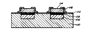
L'invention concerne une structure de semiconducteur comprenant une tranche de silicium présentant des zones de silicium, et au moins une zone de Ge¿x?Si¿1-x? se trouvant parmi les zones de silicium. Les zones de silicium et de Ge¿x?Si¿1-x? peuvent être des surfaces sensiblement coplanaires. La structure de l'invention peut comporter au moins un dispositif électronique configuré dans les zones de silicium, et au moins un dispositif électronique en matériaux des groupes III à V configuré dans la zone de Ge¿x?Si¿1-x?. La structure peut être, par exemple, un microcircuit à semiconducteur de type III-V/Si. Un autre mode de réalisation de l'invention porte sur un procédé de fabrication d'une structure de semiconducteur, consistant à se doter d'une tranche de silicium présentant une surface; à disposer des traversées dans la surface de la tranche; et à déposer dans ces traversées des zones de Ge¿x?Si¿1-x?. Le procédé peut comprendre une étape de traitement de la tranche de manière que la tranche et les régions de Ge¿x?Si¿1-x? présentent des surfaces sensiblement coplanaires. Un autre mode de réalisation de l'invention concerne un procédé de fabrication d'une structure de semiconducteur, consistant à se doter d'une tranche de silicium présentant une surface; à déposer des zones de Ge¿x?Si¿1-x? sur la surface de la tranche de silicium; et à déposer du silicium sur la surface de manière que les zones dans lesquels on a déposé du Ge¿x?Si¿1-x? soient incorporées dans le silicium.


Abrégé anglais


A semiconductor structure including a silicon wafer having silicon regions,
and at least one GexSi1-x region integrated within the silicon regions. The
silicon and GexSi1-x regions can be substantially co-planar surfaces. The
structure can include at least one electronic device configured in the silicon
regions, and at least one electronic device of III-V materials configured in
said at least one GexSi1-x region. The structure can be, for example, an
integrated III-V/Si semiconductor microchip. In accordance with another
embodiment of the invention there is provided a method of fabricating a
semiconductor structure, including providing a silicon wafer with a surface;
forming a pattern of vias within the surface of the wafer; and depositing
regions of GexSi1-x within the vias. The method can include the step of
processing the wafer so that the wafer and GexSi1-x regions have substantially
co-planar surfaces. Another embodiment provides a method of fabricating a
semiconductor structure, including providing a silicon wafer with a surface;
depositing regions of GexSi1-x to the surface of the silicon wafer; and
depositing silicon to the surface such that the deposited GexSi1-x regions are
integrated within silicon.

Revendications

Note : Les revendications sont présentées dans la langue officielle dans laquelle elles ont été soumises.


-7-
CLAIMS
1. A semiconductor structure comprising:
a silicon wafer having silicon regions; and
at least one Ge x Si1-x region integrated within said silicon regions.
2. The semiconductor structure of claim 1, wherein said silicon and Ge x Si1-x
regions
comprise substantially coplanar surfaces.
3. The semiconductor structure of claim 1 further comprising at least one
electronic
device configured in said silicon regions.
4. The semiconductor structure of claim 1 further comprising at least one
electronic
device of III-V materials configured in said at least one Ge x Si1-x region.
5. The semiconductor structure of claim 1 further comprising at least one
electronic
device of III-V materials configured in said at least one Ge x Si1-x region.
6. An integrated III-V/Si semiconductor microchip, comprising:
a silicon wafer having silicon regions;
at least one electronic device configured in said silicon regions;
at least one Ge x Si1-x region integrated within said silicon regions; and
at least one electronic device of III-V materials configured in said at least
one
Ge x Si1-x region.
7. An integrated GeSi/Si semiconductor microchip, comprising:
a silicon wafer having silicon regions;
at least one electronic device configured in said silicon regions;
at least one Ge x Si1-x region integrated within said silicon regions; and
at least one electronic device of GeSi material configured in said at least
one
Ge x Si1-x region.

-8-
8. A method of fabricating a semiconductor structure, comprising:
providing a silicon wafer with a surface;
forming a pattern of vias within the surface of said wafer; and
depositing regions of Ge x Si1-x within said vias.
9. The method of claim 8 further comprising processing said wafer so that said
wafer and Ge x Si1-x regions have substantially coplanar surfaces.
10.. A method of fabricating a semiconductor structure, comprising:
providing a silicon wafer with a surface;
depositing regions of Ge x Si1-x to said surface of said silicon wafer; and
depositing silicon to said surface such that said deposited Ge x Si1-x regions
are
integrated within silicon.

Description

Note : Les descriptions sont présentées dans la langue officielle dans laquelle elles ont été soumises.


CA 02302758 2000-03-08
WO 99/14804 PCT/US98/18715
-1 -
CO-PLANAR Si and Ge COMPOSITE SUBSTRATE
AND METHOD OF PRODUCING SAME
BACKGROUND OF THE INVENTION
The invention relates to the field of lattice-mismatched semiconductor
material
integation, and in particular to the integation of Site materials onto a Si
substrate.
As many lattice-matched devices and circuits mature, interest in lattice-
mismatched
semiconductors, devices, and circuits has increased. There are two driving
forces behind
the increased commercial interest: integation and component performance.
Integrating
dissimilar semiconductor materials on a common substrate allows the designer
to improve
performance, lower cost, and increase reliability. Thus, the most susceptible
applications
to this initial advance will be systems that require multiple types of
semiconductor materials
currently packaged separately and combined in a more conventional packaging
solution.
Examples of these applications are III-V materials integration on Si, and Site
circuit
integation with Si CMOS. Such single-chip systems are anticipated to have wide
application in communication technologies, particularly wireless
communications
technologies.
The utility of combined dissimilar semiconductors relies on the quality of the
resulting material. Large lattice-mismatch between the substrate and deposited
layer creates
2 0 stress during material deposition, creating many defects in the deposited
layer, resulting in
poor material quality and limited performance. To control threading
dislocation densities
in high mismatched deposited layers, there are only two well-established
techniques:
substrate patterning and composition gading. In the case of substrate
patterning; the idea
utilizes the knowledge that the threading dislocations are a necessity of
geometry, i.e. that
2 5 a dislocation cannot end in a crystal. If the free edge is brought closer
to another free edge
by patterning the substrate into smaller gowth areas, then it is possible to
reduce threading
dislocation densities. This technique works best for low mismatched systems in
which
dislocation nucleation is not rampant; however, it will reduce threading
dislocation densities
in high mismatched systems as well.
3 0 The other well-established technique is the use of composition gaded
layers. One
can imagine that to reach a large total mismatch, a series of low mismatched
interfaces

CA 02302758 2000-03-08
WO 99/14804 PCT/US98/18715
-2 -
could achieve great relaxation but keep threading dislocation densities low.
This result is
possible if each layer becomes substantially relaxed and is able to reuse the
threading
dislocations form the layer below. This method was long ago applied in an
empirical way
to CraAsP LEDs grown on lattice-mismatched GaAs substrates. However, after the
GaAsP
process was transferred to manufacturing, most of the subsequent lattice-
mismatch research
focussed on single. mismatched interfaces. The driving force for lattice-
mismatched
materials in applications decreased as AIGaAs/GaAs structures and InGaAsP/InP
structures
dominated optoelectronic and electronic device applications. Until these
materials systems
were fully exploited, the implementation of high mismatched layers seemed
unnecessary.
A renewed interest in graded layers has occurred due to the increased demand
for
novel components, as well as an increased demand for increased integration.
The advances
in relaxed graded Site have shown that Site devices based on relaxed Site on
Si, and the
integration of III-V materials on Si using intermediate relaxed Site graded
layers are
possible. Thus, relaxed, graded Site layers can act as the material bridge
between Site
devices and/or III-V devices and Si substrates.
These materials advances, however, are incomplete unless a proper process
sequence can be found to create these relaxed layers and subsequent devices
with relatively
standard Si circuit processing. A critical view of electronic and
optoelectronic systems
shows that the main data processing in many applications can be executed in Si
CMOS
2 0 circuits, which dominate the semiconductor industry today. To create a new
realm of Si-
based single-chip systems, a structure and process to combine Si CMOS circuits
with the
materials advances in relaxed graded Site mentioned above, is necessary.
2 5 SUMMARY OF THE INVENTION
The invention provides a method of producing a co-planar SiGe/Si substrate.
The
Site regions are formed using relaxed graded Site technology. The
planarization process
described below creates a modified Si wafer which can proceed through the Si
CMOS
process. At a convenient point in the CMOS process, the devices on or in the
Site regions
3 0 can be metallized and connected to the CMOS circuit, creating a single-
chip system utilizing
Si devices, Site devices, and/or III-V devices.

CA 02302758 2000-03-08
WO 99/14804 PCT/US98/18?15
-3 -
The invention also provides a semiconductor structure and method for producing
such a structure in which relaxed GeSi crystalline alloy surfaces can co-exist
in a planar
fashion with Si. Such a substrate is essential in harnessing the plethora of
applications in
which the integration of GeSi materials and devices, and/or III-V materials
and devices
grown on GeSi, with Si electronics is desired.
Accordingly, in accordance with one embodiment of the invention there is
provide
a semiconductor structure comprising a silicon wafer having silicon regions,
and at leap one
Ge,~Si~_X region integrated within the silicon regions. The silicon and
Ge,~Sil_X regions can
be substantially coplanar surfaces. The structure can include at least one
electronic device
configured in the silicon regions, and at least one electronic device of III-V
materials
configured in the at least one GexSi,_x region. The structure can be, for
example, an
integrated III-V/Si semiconductor microchip.
In accordance with another embodiment of the invention there is provided a
method
of fabricating a semiconductor structure, comprising providing a silicon wafer
with a
surface; forming a pattern of vies within the surface of the wafer; and
depositing regions of
Ge,~Si,_x within the vies. The method can include the step of processing the
wafer so that
the wafer and Ge,~Si~_X regions have substantially coplanar surfaces. Another
embodiment
provides a method of fabricating a semiconductor structure, comprising
providing a silicon
wafer with a surface; depositing regions of Ge,~Sil x to the surface of the
silicon wafer; and
2 0 depositing silicon to the surface such that the deposited Ge,~Sii_X
regions are integrated
within silicon.
These and other objects, features and advantages of the present invention will
become apparent in Light of the following detailed description of preferred
embodiments
thereof, as illustrated in the accompanying drawings.
BRIEF DESCRIPTION OF THE DRAWINGS
FIGS. lA-lE are a series of side views of a semiconductor structure
illustrating
the process of producing a wafer of a substrate that possesses both GeSi
alloys and Si at
3 0 the surface in accordance with the invention; and
FIG. 2 is a top view of an exemplary co-planar Si electronics/GeSi composite

CA 02302758 2000-03-08
WO 99/14804 PCT/US98/18715
-4 -
substrate configured as a microchip.
DETAILED DESCRIPTION OF THE INVENTION
FIGS. 1 A-1 E are a series of side views of a semiconductor structure
illustrating the
process of producing a wafer of a substrate that possesses both GeSi alloys
and Si at the
surface in accordance with the invention. FIG. 1 A illustrates the first
process step which
involves initially patterning a conventional Si wafer 100. Such a wafer is
usually a (001 )
orientated wafer, in which the off cut of an (001) wafer is induced by
polishing the wafer
6 degrees towards the [110] direction. The Si wafer should be patterned
lithographically
and masked such that vies 102 can be etched into the wafer. These vies will be
the areas
where the GeSi material will be deposited.
For example, the Si wafer can be coated with a layer 104 of Si02, covered wit
photoresist, and lithographically developed, producing the desired pattern in
the wafer. HF-
water or buffered etched solutions can be used then to remove the oxide from
the areas in
which the photoresist was removed. Finally, after the photoresist is removed,
the Si vies
102 can be formed by immersing the wafer in an etch solution, such as KOH,
which does
not etch Si02. The result is the formation of the Si vies. If more vertical
side-walls are
desired, for example, a dry etch can be used instead of the KOH etch step.
2 0 The wafer can then be cleaned to insure that no contamination is carried
from the
etch step into the rest of the process. The wafer is then inserted into a GeSi
deposition
system, such as a chemical vapor deposition system. As shown in FIG. 1B, a
graded GeSi
layer 106 is deposited such that the Ge composition is graded over the
thickness of the
material in the vies 102. At the end of the graded region, a uniform
composition GeSi layer
2 5 108 of the desired composition is grown such that the growth surface
traverses the Si
surface before the end of growth. This requirement will ensure that the GeSi
growth in the
via extends above the surface of the Si wafer, and also ensures that the
subsequent
planarization step does not extend into the composition graded region, located
below the
uniform layer.
3 0 The conditions used for the growth of Site should be consistent with
optimal
growth conditions for relaxed, Site graded strictures. For example, graded
layers grown

CA 02302758 2000-03-08
WO 99/14804 PCT/US98/18715
-$ -
to alloy concentrations of 30% Ge are typically grown in LTHVCVD at
temperatures
approximately 750-800C, and under reactor pressures of 25mT. Cmading rates are
typically
10% Ge per pm or less.
As shown in FIG. 1 C, the wafer can then be chemo-mechanically polished back,
so
that the uniform GeSi regions 108 are co-planar with the Si surface. If the
oxide layer is
not removed for the polishing step, it can be used as a control in the
polishing process. The
change in colors as the wafer is polished will signal the approach of the Si
wafer surface.
When the Si surface is reached, the polishing cam be ceased since the surface
is co-planar.
It will be appreciated that with this substrate, it is now possible to insert
the wafer
into a conventional Si electronics (CMOS) production line and process the Si
areas for Si
electronics. The only restriction is that the Si CMOS process might be
modified to reduce
the temperatures of the highest temperature steps. This process may be
required for the
high-Ge alloys, such as 70-100% Ge in GeSi alloys. The melting point of these
alloys
approaches that of Ge, which is 936 C. Thus, if the GeSi alloy layer is graded
to 100% Ge,
the Si CMOS processing temperatures should be reduced so that the Ge layer is
not
damaged significantly.
It will also be appreciated that other advances in improved graded Site
structures
using planarization and/or CMP can be combined with this invention to improve
the Site
material quality. For example, the process described here can be used to
create co-planar
2 0 50% Ge alloys with Si. Subsequent continued graded layer growth on the
Site areas will
result in improved Site alloys with high Ge concentrations on top of the Site
via regions.
Examples of applications are the integration of GeSi transistors with
traditional Si
CMOS circuits and devices. In this case, the GeSi areas may be graded to 30%
Ge, and the
processing temperatures of the Si CMOS process would only have to be
marginally
2 5 modified.
As shown in FIG. lE, the Si CMOS electronics are shown as regions 110, and can
include, for example, SI transistors and conventional interconnects
therebetween. ~In the
case of integrated III-V devices with Si CMOS, the alloys are generally graded
to much
higher lattice constants, e.g. 70-100% Ge. These higher Ge concentrations have
larger
3 0 lattice constants, and are therefore lattice-matched to some of the III-V
materials. Also,
in this case, it is imperative to use off cut wafers at the initiation of the
process, as described

CA 02302758 2000-03-08
wo ~n4soa rcr~s9msms
-6 -
above.
During CMOS fabrication on the Si areas, the GeSi areas can be covered with
Si02
during the entire process. After the Si CMOS is fabricated, the areas above
the GeSi can
be exposed and the Si CMOS or electronics can be protected with a passivating
mask layer
112 of oxide or nitride. Once the GeSi areas are exposed, layers 114 of III-V
materials can
be deposited, as shown in FIG. lE. One must be careful in initiating the GaAs
growth on
Ge correctly in order to prevent high dislocation densities from forniing in
the GaAs layer.
After III-V growth, the material can be defined or etched (the mask is
dissolved and lifted-
ofd, and final metallization can occur in which the III-V devices are
connected to each
other and also the Si electronics via interconnects 116, thus forming an
integrated III-V/Si
chip.
FIG. 2 is a top view of an exemplary co-planar Si electronicsJGeSi composite
substrate configured as a microchip 120. The chip includes a GeSi region 122
fabricated
as described heretofore, and a Si CMOS circuit region 124 connected to the
GeSi region
by interconnects 126.
Although the present invention has been shown and described with respect to
several preferred embodiments thereof, various changes, omissions and
additions to the
form and detail thereof, may be made therein, without departing from the
spirit and
scope of the invention.
2 0 What is claimed is:

Dessin représentatif
Une figure unique qui représente un dessin illustrant l'invention.
États administratifs

2024-08-01 : Dans le cadre de la transition vers les Brevets de nouvelle génération (BNG), la base de données sur les brevets canadiens (BDBC) contient désormais un Historique d'événement plus détaillé, qui reproduit le Journal des événements de notre nouvelle solution interne.

Veuillez noter que les événements débutant par « Inactive : » se réfèrent à des événements qui ne sont plus utilisés dans notre nouvelle solution interne.

Pour une meilleure compréhension de l'état de la demande ou brevet qui figure sur cette page, la rubrique Mise en garde , et les descriptions de Brevet , Historique d'événement , Taxes périodiques et Historique des paiements devraient être consultées.

Historique d'événement

Description Date
Inactive : CIB de MCD 2006-03-12
Demande non rétablie avant l'échéance 2004-09-08
Le délai pour l'annulation est expiré 2004-09-08
Inactive : Abandon. - Aucune rép dem par.30(2) Règles 2003-11-06
Réputée abandonnée - omission de répondre à un avis sur les taxes pour le maintien en état 2003-09-08
Inactive : Dem. de l'examinateur par.30(2) Règles 2003-05-06
Modification reçue - modification volontaire 2003-03-25
Inactive : Dem. de l'examinateur par.30(2) Règles 2002-11-25
Inactive : CIB attribuée 2002-11-19
Inactive : Grandeur de l'entité changée 2002-09-06
Inactive : Page couverture publiée 2000-05-17
Inactive : CIB en 1re position 2000-05-12
Lettre envoyée 2000-04-26
Inactive : Acc. récept. de l'entrée phase nat. - RE 2000-04-26
Demande reçue - PCT 2000-04-25
Toutes les exigences pour l'examen - jugée conforme 2000-03-08
Exigences pour une requête d'examen - jugée conforme 2000-03-08
Demande publiée (accessible au public) 1999-03-25

Historique d'abandonnement

Date d'abandonnement Raison Date de rétablissement
2003-09-08

Taxes périodiques

Le dernier paiement a été reçu le 2002-08-21

Avis : Si le paiement en totalité n'a pas été reçu au plus tard à la date indiquée, une taxe supplémentaire peut être imposée, soit une des taxes suivantes :

  • taxe de rétablissement ;
  • taxe pour paiement en souffrance ; ou
  • taxe additionnelle pour le renversement d'une péremption réputée.

Les taxes sur les brevets sont ajustées au 1er janvier de chaque année. Les montants ci-dessus sont les montants actuels s'ils sont reçus au plus tard le 31 décembre de l'année en cours.
Veuillez vous référer à la page web des taxes sur les brevets de l'OPIC pour voir tous les montants actuels des taxes.

Historique des taxes

Type de taxes Anniversaire Échéance Date payée
Taxe nationale de base - petite 2000-03-08
Enregistrement d'un document 2000-03-08
Requête d'examen - petite 2000-03-08
TM (demande, 2e anniv.) - petite 02 2000-09-08 2000-08-14
TM (demande, 3e anniv.) - petite 03 2001-09-10 2001-08-23
TM (demande, 4e anniv.) - générale 04 2002-09-09 2002-08-21
Titulaires au dossier

Les titulaires actuels et antérieures au dossier sont affichés en ordre alphabétique.

Titulaires actuels au dossier
MASSACHUSETTS INSTITUTE OF TECHNOLOGY
Titulaires antérieures au dossier
EUGENE A. FITZGERALD
Les propriétaires antérieurs qui ne figurent pas dans la liste des « Propriétaires au dossier » apparaîtront dans d'autres documents au dossier.
Documents

Pour visionner les fichiers sélectionnés, entrer le code reCAPTCHA :


Pour visualiser une image, cliquer sur un lien dans la colonne description du document. Pour télécharger l'image (les images), cliquer l'une ou plusieurs cases à cocher dans la première colonne et ensuite cliquer sur le bouton "Télécharger sélection en format PDF (archive Zip)" ou le bouton "Télécharger sélection (en un fichier PDF fusionné)".

Liste des documents de brevet publiés et non publiés sur la BDBC .

Si vous avez des difficultés à accéder au contenu, veuillez communiquer avec le Centre de services à la clientèle au 1-866-997-1936, ou envoyer un courriel au Centre de service à la clientèle de l'OPIC.


Description du
Document 
Date
(aaaa-mm-jj) 
Nombre de pages   Taille de l'image (Ko) 
Dessin représentatif 2000-05-16 1 7
Revendications 2003-03-24 3 84
Description 2003-03-24 7 354
Description 2000-03-07 6 336
Abrégé 2000-03-07 1 62
Revendications 2000-03-07 2 55
Dessins 2000-03-07 2 89
Rappel de taxe de maintien due 2000-05-08 1 111
Avis d'entree dans la phase nationale 2000-04-25 1 202
Courtoisie - Certificat d'enregistrement (document(s) connexe(s)) 2000-04-25 1 113
Courtoisie - Lettre d'abandon (taxe de maintien en état) 2003-11-02 1 176
Courtoisie - Lettre d'abandon (R30(2)) 2004-01-14 1 168
PCT 2000-03-07 10 344