Note : Les descriptions sont présentées dans la langue officielle dans laquelle elles ont été soumises.
CA 02305696 2000-03-29
WO 99/16601 PCT/US98/20420
Manufacture of Thin Metal Objects
Background of the Invention
Tn the microelectronics industry the basic method for forming circuit traces
on
a substrate involves a combination of photoresist and electroplating steps
which
incorporate many hazardous and expensive compounds and solvents and involves
extensive processing of the circuit board/substrate. One attempt to avoid the
repeated
processing of the substrate involves forming the circuit traces on a metallic
board using
the photoresist/electroplating processes or by die cutting the circuit
patterns from a
metal foil. An adhesive is then used to transfer the circuit to the substrate.
Another alternative is the "lift off' method. In this process an adhesive
image
of the circuit traces is formed on the substrate. A metal foil is then bonded
to the
adhesive image and the unwanted foil not bound to the adhesive image is then
lifted
off by an adhesive film.
These methods can be used, for example, when the substrate cannot endure the
circuit forming processes. However, the extensive processing and substantial
expense
are prohibitive to commercialization and mass production.
Brief Summary of The Invention
A novel family of compounds, commercially available as PARMODTM compositions
from Parelec, LLC, which are disclosed in Applicants' co-pending PCT
Application
PCT/US97/16226 filed 12 September 1997; the application in total being hereby
incorporated by reference. These compositions can be formulated into printing
inks or
pastes. These inks can be printed on a substrate and cured to well-
consolidated films
of pure metal in seconds. The fast curing capability of PARMOD''~'
compositions, as
well as their ready application, makes it possible to use them to create
complex thin
-1-
CA 02305696 2000-03-29
WO 99/16601 PC'T/US98/20420
metal objects by very simple and low-cost processes. An example of such an
object is
a pattern of electrical conductors used as an antenna in a radio frequency
identification
tag. Another such application is as a TAB bonding decal for semiconductors.
Electronic circuit patterns of many types can be produced by this process and
bonded
to various types of substrates and devices. the method can be used to produce
strain
gauges, thermocouples and other types of insttumentation. Many other such
objects
and applications will be evident to those skilled in the art.
The PARMODT'" compositions can be printed directly on a substrate to be used
in the final product, and it would therefore be important to obtain a good
bond to the
substrate. Furthermore, the substrate would have to withstand the temperatures
at
which the PARMOD"' compositions cure to solid metal. These requirements impose
severe restraints on the substrate materials which have to have a surface or a
coating to
which PARMODT"' will bond and have to have high temperature capability: Both
requirements tend to limit the selection and increase the price of the
substrate. This is
particularly difficult in that the low cost copper PARMODT"" mixture requires
the
highest cure temperature and is limited to expensive polyimide substrates.
The present invention decoupies the curing and adhesion processes from the
substrate by doing the printing and curing on a temporary substrate and then
transferring the metal foil object produced to a permanent substrate at low
temperature.
Desired characteristics of the temporary substrate are: that the PARMOD'''~'
not
permanently bond to it: that it have approximately the same coefficient of
thermal
expansion as the PARMODT"'; that it withstand the temperature at which the
PARMODT"' cures; and, that it be easily reusable or very inexpensive.
The preferred PARMODT" compounds contain a Reactive Organic Medium
(ROM) and a source of metal, preferably metal flakes, metal powders and their
mixtures. The ROM consists of either a Metallo-Organic Decomposition (MOD)
compound or an organic reagent which can form such a compound upon heating in
the
presence of the metal source. The ingredients are blended together with
Theology
modifying organic vehicles well known in the art, if necessary, to produce
printing
inks or pastes. These inks can be printed on a substrate and cured to well-
consolidated
films, traces and objects of pure metal in seconds.
-2-
CA 02305696 2000-03-29
WO 99116601 PCTNS98/20420
The process can be performed continuously, for example, using belts and tapes
or webs. Likewise, using a series of belts, tapes and webs, multilayered units
can be
produced
Brief Description of the Drawings
Preferred embodiments according to the present invention will be described in
detail with reference to the following figures, wherein:
Figure 1. is an illustration of a continuous process using the method of the
invention
to foam substrates having metal circuit traces, components, and objects.
Figure 2 is an illustration of a continuous process using the method of the
current
invention to form multilayered circuits.
Figure 3. Is an illustration of a tape automated bonding decal formed using
the current
method.
Detailed Description of the Invention
Preferred compositions useful for forming the traces, components and objects
are comprised of a metal mixture and a Reactive Organic Medium (ROM). These
compositions can be applied to thermally stable substrates and cured to well-
consolidated circuit traces and objects by heat treatment. The compositions
exhibit a
critical temperature above which they undergo a transformation to well-
consolidated
electrical conductors with a resistivity only two to four times the bulk
resistivity of the
metal in question. The electrical conductivity is equal to that obtained by
conventional
high temperature metal powder sintering in conventional thick film
compositions on
ceramic substrates. Remarkably, this consolidation process takes place at
temperatures
400 to 500 degrees Celsius lower than with compounds conventionally used in
thick
film technology, and in times which are an order of magnitude shorter than are
required for sintering.
-3-
CA 02305696 2000-03-29
WO 99/16601 PCT/US98120420
Suitable metals include copper, silver, gold, zinc, cadmium, palladium,
iridium,
ruthenium, osmium, rhodium, platinum, iron, cobalt, nickel, indium, tin,
antimony,
lead, bismuth and mixtures thereof. Examples of typical proportions of
PARMOD'''"'
mixtures containing an organic acid as the ROM and both metal flakes and
colloidal
metal powder are illustrated in Table 1 as follows:
TABLE 1 Acid-Bssed PARMODT"'
Metal FlakeMetal PowderOrganic Organic
acid vehicle
Range 20-60% 10-45% I S-35% 0-35%
Preferred 40-60% 24-44% 5-20% I O-10%
Most preferred40-60% 24-44% 10-20% 0-5%
Percents by total weight of the composition.
In a preferred embodiment, the metal mixture contains metal flake and
colloidal or semi-colloidal metal powder where the total of flake plus powder
is
preferred to be 60-85% of the total mixture, and the powder is preferred to be
30-50%
of the total metal. Larger amounts of organic vehicle may be added to reduce
viscosity
for certain applications.
The metal flakes have a major dimension between 2 to 10 micrometers,
preferably about 5 micrometers, and a thickness of less than 1 micrometer.
They can be
produced by techniques well known in the art by milling the corresponding
metal
powder with a lubricant, which is frequently a fatty acid or fatty acid soap.
The starting
powders are usually produced by chemical precipitation to obtain the desired
particle
size and degree of purity. The flakes are sold for electronic applications as
constituents
of thick film inks and silver-loaded conductive epoxies.
The flakes perform several functions. They form a skeleton structure in the
printed image which holds the other ingredients together and prevents loss of
resolution when the mixture is heated to cure it. The flakes naturally assume
a lamellar
-4-
CA 02305696 2000-03-29
WO 99!16601 PCTNS98/20420
structure like a stone wall which provides electrical conductivity in the
direction
parallel to the surface of the substrate and provides a framework to lessen
the amount
of metal transport necessary to achieve the well-consolidated pure metal
conductors
which are the objective of this invention. They also provide low surface
energy, flat
surfaces to which the other constituents of the composition can bond.
The other metallic powder mixture constituent of the present invention are
preferably colloidal or semi-colloidal powders with individual particle
diameters below
about 100 manometers, preferably less than about SO manometers. The colloidal
or
semi-colloidal powder is preferably present in about 40% by weight of the
total weight
of the metal powder mixture. A primary fitnction of these powders is to lower
the
temperature at which the compositions will consolidate to nearly solid pure
metal
conductors. The presence of fine metal powder has been found to be helpful in
advancing this low temperature process with silver and essential to the
consolidation of
copper mixtures. It is important that they be present as individual particies.
Metal
particles this small have a strong tendency to agglomerate into aggregates
with an open
skeletal structure.
Colloidal silver particles with a nominal diameter of 20 manometers were
shown to have an excellent state of dispersion and have been used in silver
compositions and lowered the critical consolidation temperature from 300 to
260
degrees C.
To achieve and preserve the desired degree of dispersion of colloidal metal it
is
essential to stabilize the particles so that they cannot aggregate. In the
case of the silver
particles they were stabilized by the presence of a surfactant which coated
the surface
of the particles and prevented metal-to-metal contact. Suitable surfactants
include
carboxylic acids and metal soaps of carboxylic acids. This favors chemical
precipitation as a means of producing the powders, since they can be exposed
to an
environment which promotes stabilization from formation to final
consolidation.
The Reactive Organic Medium (ROM) provides the environment in which the
metal mixture is bonded together to form well-consolidated conductors. Many
classes
of organic compounds can fimction as the ROM. The common characteristic which
-5-
CA 02305696 2000-03-29
WO 99116601 PCT/US98IZ0420
they share and which renders them effective is that they have, or can form, a
bond to
the metal via a hetero-atom. The hetem-atoms can be oxygen, nitrogen, sulfur,
phosphorous, arsenic, selenium and other nonmetallic elements, preferably
oxygen,
nitrogen or sulfur. This bond is weaker than the bonds holding the organic
moiety
together, and can be thermally broken to deposit the metal. In most cases the
reaction
is reversible, so that the acid or other organic residue can react with metal
to reform the
metallo-organic compound, as shown schematically below:
R-M t~R + M
where R is a reactive organic compound and M is the metal.
As an illustration of PARMODT'" mixtures containing MOD forming
constituents such as organic acids, the reactions which take place in curing
are as
follows:
lIa.) Acid + Metal powder ~ MOD + H2
or
IIb) Acid + Metal Oxide ~ MOD + H20
and
IIn MOD + heat + H20 r~ Bulk metal + Acid
The effect is to consume the small particles and weld together the big ones to
create macroscopic circuit conductors of pure metal. In place of acid, some
other active
organic reagent which will produce an easily decomposed metallo-organic
compound
from either the oxide or the metal could be used. An example would be the use
of
sulfur compounds to make mercaptides or nitrogen ligands to produce
decomposable
complexes.
Examples of useful compounds are soaps of carboxylic acids, in which the
hetero-atom is oxygen; amino compounds, in which the hetero-atom is nitrogen;
and
mercapto compounds, in which the hetero-atom is sulfur.
-6-
CA 02305696 2000-03-29
WO 99/16601 PCT/US98/20420
Specific examples of preferred ROM constituents are the carboxylic acids and
the corresponding metallic soaps of neodecanoic acid and 2-ethyl hexanoic acid
with
silver and copper, such as. silver neodecanoate illustrated by the formula:
0 R~
Ag-O-C - ~ -R~
R3
where R 1 , R2 , and R 3 are C9H 19
and silver 2-ethyl hexanoate as illustrated by the formula:
0 C2H$
Ag-0 _ C -CH_C3H7
Gold amine 2-ethyl hexanoate is an example of a nitrogen compound.:
H
''"7H15 C 0
0 0 H3C
C~H~5 C-0-Au ~ CH
0
C7H,~ C=0 N
GZHS
Gold amine 1-ethyl hexanoate (gold amine octoate)
_7_
CA 02305696 2000-03-29
WO 99/16601 PCT/US98/20420
Gold t-dodecyl mercaptide is an example of a sulfur compound:
R1
Au-S-C-R2
R3
where R1 , R2 , and R3 are C11H23
These ROM compositions can be made by methods well known in the art. All
of the above compounds are capable of decomposition to the respective metals
at
relatively low temperatures. For the silver neodecanoate and silver 2-ethyl
hexanoate
(silver octoate), the decomposition temperature is between 200 and
250°C . For the
corresponding copper compounds, it is between 300 and 315 C. Gold sulfides
decompose at very low temperatures in the neighborhood of 150°C . Gold
amine
octoate decomposes between 300 and 500°C . The copper and silver
compounds can
be reformed from the corresponding acids at the same temperature, so the
reaction is
reversible, as mentioned above.
In some cases it is convenient to add theology-enhancing compounds well
known in the art to improve the printing characteristics of the compositions
of the
invention. Alpha-terpineol has been used to reduce the viscosity of copper and
silver
compositions to facilitate screen printing. Alpha-tetpineol also participates
in the
consolidation reaction by virtue of the acid character of the OH group bonded
to an
unsaturated ring. By selecting constituents and additives, it has proven
possible to
produce a range of printable compositions ranging from fluid inks with a
viscosity of
15 centipoise to solid powders.
The composition is printed on the substrate using any convenient printing
technology. Screen printing and stenciling are suitable for rigid substrates
in relatively
small numbers with high resolution. Gravure printing, impression printing and
offset
printing are suitable for high production rates on flexible substrates. Ink
jet printing
and electrostatic printing offer the additional advantage of direct computer
control of
the printed image. This permits circuits to be printed directly from Computer
Aided
_g_
CA 02305696 2000-03-29
WO 99/16601 PGT/US98lZ0420
Design (CAD) files and eliminates the need for special tooting. Each circuit
can be
different, if desired, for coding or prototyping. The same end can be achieved
at lower
production rates with computer- controlled dispensing equipment. This
equipment
produces dots or lines by moving a needle over the surface and dispensing
printing
composition supplied by a pump or pressurized syringe.
Compositions of this invention have been applied by screen printing,
stenciling, dispensing, gravure printing, ink jet printing, impression
printing, offset
printing and electrostatic printing. Alternative application methods include
coating an
adhesive pattern with a dry powder composition or toner. Screening, as used in
applying conventional thick film pastes has been used most extensively for
preparing
samples for evaluation. A composition with a viscosity of approximately 500
poise is
forced through a fine screen with a photo-defined open image of the desired
conductor
pattern in it by a rubber squeegee. The resolution which has been achieved by
this
method is approximately 125 micron (5 mil) lines and spaces, although
production
screen printers can achieve patterns as fine as 50 microns. Conductive traces
with
thicknesses up to 50 microns have been printed, though most of the test
patterns have
been in the neighborhood of 12 microns thick, which is equivalent to 0:37
ounces of
copper per square foot.
When the metallo-organic decomposition compound or the acid from which it
is formed is mixed with the metal flake and colloidal metal powder
constituents
described above. printed as a relatively thin layer on an appropriate
substrate, and
heated to a critical temperature above the decomposition temperature of the
metallo-
organic compound, a reaction takes place which results in the sudden
consolidation of
the loosely aggregated metal constituents into a nearly solid metal trace with
greatly
reduced electrical resistivity. Scanning Electron Micrograph cross sections of
traces
which have been heated to decompose the metalio-organic compound but below the
critical temperature for copper and for silver mixtures show the individual
metal
flakes and powder particles, much like a picture of the unheated mixture.
When the traces are heated above the critical temperature, there is a very
rapid
decrease in electrical resistivity, a dramatic increase in mechanical cohesive
strength of
-9-
CA 02305696 2000-03-29
WO 99/16601 PCT/US98/20420
the deposit and the appearance of the deposits changes. SEM cross sections of
copper,
silver and gold mixtures that have been heated above the critical temperature
show that
the metal flake and powder have consolidated into a bonded network of solid
metal.
The compositions are cured by exposure to heat for a short period of time.
'This
time varies with the temperature to which the substrate can safely be exposed,
but is
less than a minute to achieve most of the electrical conductivity of which the
composition is capable, and in some cases is less than 10 seconds at
temperature.
For copper (and gold) the critical temperature is in excess of 300°C .
Between
305 and 325°C the resistivity of copper traces dropped by a factor of
100 to a value
below 10 microohm-cm. The bulk resistivity of copper is 1.7 microohm-cm. At
the
same temperature at which the resistivity drops the mechanical properties of
the traces
improved equally dramatically. From being brittle and poorly adherent as
measured by
creasing the samples and pulling the traces offwith Scotch Tape the samples
become
ductile enough to survive a sharp 180 degree crease in the 75 micron (3 mil)
substrate
followed by tape testing. The crease test is equivalent to an elongation of
the metal
trace of 17%. The tape test is equivalent to an adhesion of approximately 10
Newtons/cm (6 Ib per lineal inch) Heating to still higher temperatures
decreases the
resistivity only slightly.
For silver, the decreasc in resistivity with processing temperature is not as
dramatic as with copper but the conversion from a poorly-consolidated material
which
is easily fragmented to a ductile metal is equally sharp. The critical
temperature is
approximately 230°C .
The critical temperature can be adjusted by mixing metaIlo-organic
constituents. As mentioned above, gold amine octoate decomposes at
temperatures up
to 500°C . This is too high for use with polymer-based printed circuit
substrates or
most other electronic components. Gold t-dodecyl mereaptide decomposes at
approximately 150°C . This is too low to bond effectively with the
substrates of
interest or with added gold flake. Gold neodecanoate decomposes at about 120-
154°C.
A mixture of gold amine octoate and gold neodecanoate has been used to achieve
a
decomposition temperature in the desirable range.
-10-
CA 02305696 2000-03-29
WO 99116601 PCT/US9820420
Both gold and silver mixtures can be heated in air since the elemental metals
are the stable form at the temperature at which the metallo-organic
constituent
decomposes. Copper, however, requires the use of a protective atmosphere to
prevent
the formation of copper oxide which is the stable product of decomposition in
air. A
nitrogen atmosphere containing Iess than about 20 and most preferably less
than 3 ppm
by volume of oxygen has been found to be suitable. Addition of water vapor in
the
amount of about 5% has proven to be helpful in improving the conductivity of
the
resulting deposits.
lNhile the PARMODT"' should not bond to the thermally stable substrate, a
certain amount of tackiness or adhesion may be desired when using an
automated,
continuous process. Substrates well known in the art will possess the
characteristics
required for the temporary substrate. Examples of suitable temporary
substrates
include, but are not limited to, polyimide films, polysolfone films, polyester
films,
teflon coated films, silicone coated films; metal foils, glass and ceramic
surfaces.
The permanent substrate need only have the ability to bond reliably to the
transferred metal foil in addition to any other requirements of the final
application such
as dielectric strength. Examples of suitable substrates include, for example,
polyethylene, polypropylene, polystyrene, polyester, polycarbonate,
polyurethane,
cellulose and paper. Coatings of pressure sensitive or other types of adhesive
known
in the art may be used to accomplish this, for example, thermoplastic
materials such as
polyethylene or epoxy, phenolic, acrylic and polyimide thermosetting resins.
It may
also be accomplished by the thetrnoplastic or adhesive nature of the substrate
itself, for
example, polyethylene, polypropylene or polystyrene.
For still greater economies and higher production rates, the conductor pattern
can be applied to a continuous web of substrate by a rotary press, much like
printing a
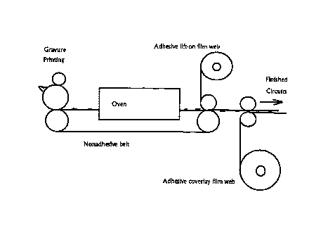
newspaper but with finer resolution, as shown in Figure 1. Gravure printing
can be
used in this application. Offset printing can produce very high resolution
also. Ink jet
printing and electrostatic printing at high speeds are candidates. Following
the printing
step, the circuits will be cured in an oven, still as a continuous web. The
ability of
these mixtures to cure to solid metal in seconds is critical to realizing this
concept.
- 11 -
CA 02305696 2000-03-29
WO 99/16601 PCT/US98/20420
Longer processing times would make the oven disproportionately large relative
to the
press and squander much of the speed advantage of high speed printing. In a
continuos
process the PARMODT"" compound is printed in the desired patterns onto a belt
of the
thermally stable substrate. The belt passes through an oven in which the
PARMODT"'
is cured and forms solid metal objects. An adhesive face of a continuous
"tape" of the
permanent substrate is contacted with the belt and the metal objects are
"lifted" onto
the permanent substrate tape. The tape can then be laminated and cut to form
individual circuit boards.
Multiple layers can readily be produced by this technology by using a double
sided coverlay which will lift-off another set of images as illustrated in
Figure 2. A
double sided dielectric is used to cover one layer and lift the metal objects
onto the
next layer. This double-sided dielectric can be, for example, a conventional
prepreg
consisting of glass cloth reinforcement impregnated with B-stage epoxy resin.
The
process may be continued for as many layers as desired to make multilayer
circuit
boards by a continuous, low-cost process.
Long term, for very high production runs, the newspaper analogy can be
pushed further with multiple rotary presses turning out multiple metal objects
simultaneously which are cured in a single oven and perhaps joined and
laminated on
the fly before die cutting to size. The stacks would be cut apart to create
individual the
circuits. A still less expensive approach is to use the adhesive on the back
surface of
single sided inner layers to laminate the stack without the use of prepreg.
The lift-on process can also be used to make partially supported patterned
metal foil objects such as Tape Automated Bonding Decals. The pattern is
printed on a
nonadhesive material and lifted onto a die cut adhesive tape leaving part of
the pattern
exposed. The result is a tape with fine metal fingers which can be gang bonded
to the
pads on semiconductor chips. The outer ends of the fingers which are supported
by the
tape can be soldered to a semiconductor package or direct to a printed circuit
for chip-
on-board mounting. Such a TAB decal is shown schematically in Figure 3.
-12-
CA 02305696 2000-03-29
WO 99/16601 PCT/US98I20420
Other supported, partially supported and unsupported objects can be made by
the technology of the present invention as can be appreciated by those skilled
in the
relevant arts. examples are:
Instrumentation such as thermocouples and strain gauges
Resistors, capacitors and inductors printed on polymer films
Electric heaters
Circuitry comprising any or all of the above, such as radio frequency tags
which can be interrogated remotely for identification of packages and baggage
Decorative metallic items such as jewelry and Christmas ornaments
Examples
The examples described below indicate how the individual constituents of the
preferred compositions and the conditions for applying them function to
provide the
desired result. The examples will serve to further typify the nature of this
invention,
but should not be construed as a limitation in the scope thereof. which scope
is defined
solely in the appended claims.
Example 1
A silver PARMODT'" screen ink was prepared as follows. 12.0 grams of
Degussa silver flake, 3.0 grams of silver neodecanoate, and 1.35 grams of
neodecanoic
acid were mixed together using a spatula. The resulting mixture was then
milled on a
roll mill to give a homogeneous paste.
Images of an eight turn antenna coil and a capacitative plate were screen
printed on separate substrates using silver PARMOD screen . The screen
parameters
were a 195 mesh screen backed with a 0.7 mil emulsion. The substrates used
were 1
mil thick sheets of ICaladex~ 2030 polyethylene naphthalate (PEI. The samples
were thermally cured by heating to 210oC in a box furnace with an air
atmosphere for
- 13 -
CA 02305696 2000-03-29
WO 99/16601 PGT/US98/Z0420
2-5 minutes. The resulting samples were continuous pure silver films with an
electrical resistivity of 3.5 p.S2-cm and poor adhesion to the substrate.
The silver films were then transfer laminated to opposite sides of a 1.3 mil
thick polyethylene (PE) substrate. The PE substrate was placed over the silver
eight
turn antenna coil. The silver capacitative plate was placed face down on the
PE and
aligned with the silver image below. The sample was then hot pressed with a
220oC
iron. The two PEN film substrates were then carefiiily peeled away leaving the
silver
films transferred in tact on either side of the PE substrate. After transfer,
the electrical
resistivity properties remained the same.
Example 2
The procedure of Example 1 was repeated except that only the capacitative
plate was screen printed and thermally cured using the silver screen ink
prepared in
Example 1. The eight tum antenna coil was etched aluminum on a 1 mil thick PE
substrate. The silver capacitative plate was transfer laminated to the
aluminum coil as
was done in Example 3 with similar results.
Ezample 3
The procedure of Example 2 was repeated except that the capacitative plate was
printed and thermally cured on a DuPont Kapton~ H polyimide film. Similar
results
were obtained with the transfer lamination.
Example 4
The procedure of Example 2 was repeated except that the cagacitative plate was
printed and thermally cured on a DuPont Kapton~ FN FEP Teflon coated polyimide
film. Similar results were obtained with the transfer lamination.
-14-
CA 02305696 2000-03-29
WO 99/16601 PCT/US98I20420
Example 5
Copper PARMODTM ink was prepared by mixing 47 grams of copper flake,
29 grams of nanometer sized spherical copper powder mixed with neodecanoic
acid
(~77 wt% metal) and 1 S grams of neodecanoic acid in a glove box. This premix
was
than further mixed on a 2-roll mill for 30 minutes in air. The gap setting on
the mill
was 0.006" - 0.008". After milling, the ink was removed from the mill and
stored in a
plastic syringe from which is also was dispensed.
The copper PARMODTM ink was screened onto aluminum foil and fired at
360oC for 3 minutes in a N2-H20-H2 gas mix. The resulting copper circuit
produced
did not adhere well to the aluminum foil substrate. The resulting circuit was
peeled off
the substrate using 2 inch wide pressure sensitive, adhesive coated cellophane
tape
which was then stuck to a paper backing.
Example 6
Copper PARMODTM ink was prepared by mixing 49 grams of copper flake,
31 grams bf nanometer sized spherical copper powder mixed with neodecanoic
acid
(~77 wt% metal) and 11 grams of neodecanoic acid in a glove box. This premix
was
than further mixed on a 2-roll mill for 30 minutes in air. The gap setting on
the mill
was 0.006" - 0.008". After milling, the ink was removed from the mill and
stored in a
plastic syringe from which is also was dispensed.
An aqueous suspension of boron nitride powder was sprayed onto an alumina
substrate (0.030" thick) and allowed to dry in air. Excess boron nitride was
removed by
wiping with a lint free cloth.
The copper PARMODTM ink was screened onto the boron nitride coated
alumina substrate in the form of an antcnna coil.for a radio frequency tag and
fired at
360oC for 3 minutes in a N2-H20-H2 gas mix. The resulting antenna coil did not
adhcre well to the alumina substrate and it was transferred to a 0:004 "
polyester sheet
coated with pressure sensitive adhesive. The same process was repeated for the
- 15 -
CA 02305696 2000-03-29
WO 99/16601 PC1'IUS98/20420
capacitor portion of the tag, and the antenna coil and the capacitor were then
"laminated" together using rubber cement deposited on both sides of Kapton,
which
serves as the dielectric.
Eznmple 7
Copper PARMODTM ink was prepared by mixing 48 grams of 9 micron
diameter spherical copper powder, 30 grams of 3 micron diameter spherical
copper
powder, 15 grams of nanometer sized spherical copper powder mixed with
neodecanoic acid (-77 wt% metal) and 7 grams of neodecanoic acid in a glove
box.
This premix was than furtheFmixed on a 2-roll mill for 30 minutes in air. The
gap
setting on the mill was 0.006" - 0.008". After milling, the ink was removed
from the
mill and stored in a plastic syringe from which is also was dispensed.
The copper PARMODTM ink was screened onto unclad Teflon-glass laminate
(0.062" thick) and fired at 300oC for 6 minutes in a N2-H20-H2 gas mix. The
resulting copper circuit produced did not adhere well to the Teflon-glass
laminate case
of the epoxy-glass.
The copper circuit on the Teflon-glass rigid board was transferred to a rigid
FR-4 glass-epoxy substrate by lamination using an acrylic sheet adhesive
(DuPont
LF0120). An epoxy prepare was used to adhere the Kapton to the FR-4 board. The
lamination conditions were 350 Psi laminating pressure and a vacuum of 28 in
Hg for
60 minutes at 190oC. The resulting bright copper circuit was well adhered to
the
Kapton. After submersion in a 255oC solder bath for 20 seconds, there were na
signs
of delimitation, and the solder adhered well to the copper, which had been
immersed in
flux prior to being introduced into the solder bath.
-16-
CA 02305696 2000-03-29
WO 99/16601 PCT/US98/Z0420
Eiample 8
Copper PARMOD'~'' ink was prepared by mixing 48 grams of 9 micron
diameter spherical copper powder, 30 grams of 3 micron diameter spherical
copper
powder, 15 grams of manometer sized spherical copper powder mixed with
neodecanoic acid (~ 77 wt% metal) and 7 grams of neodecanoic acid in a glove
box.
This premix was then further mixed on a 2-roll mill for 30 minutes in air. The
gap
setting on the mill was 0.006" - 0.008". After milling, the ink was removed
from the
mill and stored in a plastic syringe from which it also was dispensed.
Copper PARMOD"'' ink was screened onto unclad Teflon-glass laminate
(0.062" thick) and fired at 300°C for 6 minutes in a Na-Ha0-Hz gas mix.
The resulting
copper circuit produced did not adhere well to the Teflon-glass laminate.
The copper circuit on the Teflon-glass rigid board was transferred to a rigid,
glass-polyester substrate by lamination using an acrylic sheet adhesive
(DuPont
LF0120). The lamination conditions were 350 Psi lamination pressure and vacuum
pressure of 28 in Hg for 60 minutes at 190°C. The resulting bright
copper circuit was
well adhered to the acrylic. After submersion in a 255°C solder bath
for 20 seconds,
there were no signs of delamination, and the solder adhered well to the
copper, which
had been immersed in flux prior to being introduced into the solder bath.
While the invention has been described with reference to preferred
embodiments thereof, it will be appreciated by those of ordinary skill in the
art that
modifications can be make to the structure and form of the invention without
departing
from the spirit and scope thereof.
- 17 -