Sélection de la langue

Search

Sommaire du brevet 2305727 

Énoncé de désistement de responsabilité concernant l'information provenant de tiers

Une partie des informations de ce site Web a été fournie par des sources externes. Le gouvernement du Canada n'assume aucune responsabilité concernant la précision, l'actualité ou la fiabilité des informations fournies par les sources externes. Les utilisateurs qui désirent employer cette information devraient consulter directement la source des informations. Le contenu fourni par les sources externes n'est pas assujetti aux exigences sur les langues officielles, la protection des renseignements personnels et l'accessibilité.

Disponibilité de l'Abrégé et des Revendications

L'apparition de différences dans le texte et l'image des Revendications et de l'Abrégé dépend du moment auquel le document est publié. Les textes des Revendications et de l'Abrégé sont affichés :

  • lorsque la demande peut être examinée par le public;
  • lorsque le brevet est émis (délivrance).
(12) Brevet: (11) CA 2305727
(54) Titre français: AMELIORATIONS DU RENDEMENT QUANTIQUE DANS DES DETECTEURS DE PIXELS ACTIFS
(54) Titre anglais: QUANTUM EFFICIENCY IMPROVEMENTS IN ACTIVE PIXEL SENSORS
Statut: Durée expirée - au-delà du délai suivant l'octroi
Données bibliographiques
(51) Classification internationale des brevets (CIB):
  • H04N 3/14 (2006.01)
  • H01L 27/146 (2006.01)
  • H01L 27/148 (2006.01)
(72) Inventeurs :
  • FOSSUM, ERIC (Etats-Unis d'Amérique)
(73) Titulaires :
  • MICRON TECHNOLOGY, INC.
(71) Demandeurs :
  • MICRON TECHNOLOGY, INC. (Etats-Unis d'Amérique)
(74) Agent: MBM INTELLECTUAL PROPERTY AGENCY
(74) Co-agent:
(45) Délivré: 2004-05-25
(86) Date de dépôt PCT: 1998-10-05
(87) Mise à la disponibilité du public: 1999-04-15
Requête d'examen: 2001-08-01
Licence disponible: S.O.
Cédé au domaine public: S.O.
(25) Langue des documents déposés: Anglais

Traité de coopération en matière de brevets (PCT): Oui
(86) Numéro de la demande PCT: PCT/US1998/020884
(87) Numéro de publication internationale PCT: WO 1999018717
(85) Entrée nationale: 2000-04-06

(30) Données de priorité de la demande:
Numéro de la demande Pays / territoire Date
08/944,794 (Etats-Unis d'Amérique) 1997-10-06

Abrégés

Abrégé français

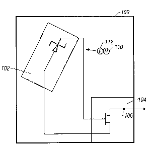
L'invention concerne le rendement quantique dans un détecteur de pixels actif (100), qu'on peut améliorer par un dimensionnement et un formage appropriés des éléments de contact. Les éléments à photodiodes (102) présentent des formes spéciales qui sont optimisées pour obtenir une charge diffusée plutôt qu'une charge directe. Des grilles photoniques (Fig. 11) sont formées avec un revêtement en polysilicium aminci.


Abrégé anglais


Quantum efficiency in an
active pixel sensor (100)
improved by proper sizing and
shaping of the contacts. The
photodiode elements (102) are
formed of special shapes that
are optimized for obtaining
diffusion of charge, rather than
obtaining the charge directly.
Photogates (Fig. 11) are formed
with a thinned polysilicon
covering.

Revendications

Note : Les revendications sont présentées dans la langue officielle dans laquelle elles ont été soumises.


-8-
What is claimed is:
1. An image sensor, comprising:
a plurality of pixel areas, each pixel area
including a circuitry area and a photodiode area,
said photodiode area including a photodiode element
therein, said photodiode element taking less than an
entire amount of space left open by the circuitry
area.
2. A sensor as in claim 1 wherein said photodiode is
located in a position on said substrate which
includes a plurality of collection areas in said
substrate which are substantially equidistant from
said photodiode.
3. A sensor as in claim 2 wherein said photodiode is in
the shape of a bar extending from an edge of the
pixel towards a center of the pixel.
4. A sensor as in claim 2 wherein said photodiode is in
the shape of a portion of a ring.
5. A sensor as in claim 2 wherein said photodiode
extends along a diagonal of said pixel.
6. A sensor as in claim 2 wherein said photodiode is in
the shape of a ring, a center of the ring being a
center of the pixel.
7. A sensor as in claim 2 wherein said photodiode is in
the shape of an H.
8. A sensor as in claim 2 wherein said photodiode is in
the shape of an X.

-9-
9. An image sensor as in claim 1, wherein said photodiode element is formed
of an opaque material.
10. An image sensor as in claim 9, wherein said photodiode element is formed
of polycide.

Description

Note : Les descriptions sont présentées dans la langue officielle dans laquelle elles ont été soumises.


CA 02305727 2000-04-06
-WO 99/18717 PCT/US98/20884
-1-
TITLE OF THE INV~'NTION
QUANTUM BFFICIBNCY IMPROVEMENTS IN ACTIVE PIXEL SENSORS
BACKGROUND OF THE INVENTION
The present invention describes to a technique of
S optimizing quantum efficiency in a CMOS image sensor,
specifically an active pixel sensor.
Electronic image sensors obtain an electrical image
of a subject. The sensor converts the incaming light
photons to an electronic signal (electrons). The effi-
ciency of conversion between the photons and electrons is
often called quantum efficiency ("QE"). QE is one of the
key imaging performance benchmarks of sensors.
CCD type light sensors store charge in an array
formed on a substrate. Each portion of the array stores a
picture element, or "pixel" of the overall image.
Sensors formed of complementary metal oxides
semiconductor ("CMOS") include associated circuitry within
the pixel. That associated circuit portion is not light
sensitive. Those areas which do not collect light include
the associated circuitry which operates to convert the
information stored in the pixel into an electronic signal.
These non-photosensitive areas include, but are not limited
to, routing buses, transistors, and areas covered by opaque
materials such as silicides.
Many image sensor devices convert the incoming
photons to charge using a photogate. That charge is stored
in the substrate. Other devices convert the incoming
photons to electrons using a photodiode. However, the
photodiode must therefore receive the photons in order to
convert them. Therefore, it has been the understanding of
those of ordinary skill in the art that the non-light

CA 02305727 2003-04-16
-2-
sensitive areas would reduce the overall quantum efficiency
of the device and hence, the overa~.l light sensitivity of
the device. Therefore, those having ordinary skill in the
art have tried to minimize the am~~unt of the pixel area
which was used for associated circuitry, in order to
maximize the photosensitive area. This was done by, for
example, enlarging the size of the photodiode to maximize
the amount of light received thereby.
Another common trend in the art has been to use a
combination of polysilicon and metal to reduce the resis
tance of electricity. The polysilicon and metal combina
tion is often called a pol~Pcide. Specific materials
include silicides and salacides. Many modern sub-micron
processes use these materials ire order to reduce the
resistance. However, these materials are als:~ opaque.
Diodes, ineludi.ng the phutodiades which can be used
in active pixel sensors, can be formed of suc~z a polycide.
However, to the knowledge or the inventors, no cane has
suggested doing so, since the photudiode forme~~ of polycide
would be opaque arnd therefore would not be expected to
receive information from the incoming light.
A basic active pixel sensor is shown in U.S. Patent
No. 5,4'71,51~~
SL1MMAF~,Y OF THE INVFN'rION
The present invention describes a technique that
improves quantum efficiency in a GMc~S sensor. This is done
according to the present invention using different tech-
niques. A first technique describes improving the QE in a
photodiode pixel by reducing, rather than increasing, the
amount_ of photosensitive area :;gin the pixel.
A second technique desc:xpibes improving the QE
response of a photogate structure"

CA 02305727 2000-04-06
WO 99/18717 PCT/US98/20884
-3-
An aspect of the present invention involves making
the photodiode smaller, instead of larger as was suggested
by the prior art. This is done by using the inventor's
understanding of a new technique of operation. Photons are
captured in the substrate of the photodiode and are con-
verted to electron-hole pairs. These electron-hole pairs
diffuse into the diode to form current. The diode size
according to this embodiment is optimized for obtaining
diffusion from the substrate, rather than for obtaining the
light directly. This requires that the diode be smaller
than the overall open area in the substrate.
Another aspect of the present invention includes the
special shapes for these photodiodes which reduce their
capacitance and further increase their gain.
Another aspect of the present invention is using a
thinned polysilicon layer overlying a photogate structure.
This thinned polysilicon layer avoids certain photon
attenuation.
HRIEF DESCRIPTION OF THE DRAWINGS
The drawings include:
Figure 1 shows an active pixel sensor using a
photodiode device;
Figures 2-6 show different possible shapes for the
photodiodes:
Figure 7 shows and exemplary response of active
pixel sensor;
Figure 8 shows a photodiode formed of polycides;
Figures 9 and 10 show two additional shapes for
photodiodes of the present invention; and
Figure 11 shows a photogate device with a thin
polysilicon overlayer.

CA 02305727 2000-04-06
WO 99/18717 PG"T/US98/20884
-4-
DESCRIPTION OF THE PREFERRED EMBODINIBNTS
Fig. 1 shows a schematic representation of a
photodiode pixel. Each pixel 100 includes a photodiode
area 102 and associated circuitry area 104. The device
shown in Fig. 1 is an "active pixel" which means that each
pixel includes at least some circuitry associated with the
pixel and actually formed within the pixel. Circuitry 104
is shown schematically as including a source follower, but
it should be understood that other associated circuitry can
also be integrated in the pixel. That associated circuitry
is preferably formed of NMOS or CMOS. NMOS is preferred
since CMOS circuits would be larger in size. No special-
ized semiconductor formation techniques are required to
form either NMOS or CMOS, such as those required with
charge coupled devices ("COD's"). More details about this
are found in U.S. Patent No. 5,471,515.
The photodiode element 102 is also shown in Fig. 1.
Photodiode 102 is formed of a CMOS-compatible process, such
as CMOS or NMOS. Fig. 1 shows a system according to the
present invention whereby the size of the photodiode 102
is smaller than the total area within the pixel which is
available for such a photodiode.
The established teaching in the art of image sensors
and especially active pixel sensors has been that the
photodiode pixel should have a photon collecting area which
is as large as possible. Conventional photodiode pixels
have formed the photodiode in the shape of a solid polygon
such as a square, rectangle, or L-shaped photodiode area.
For example, in the exemplary pixel layout shown in Fig. 1,
the photodiode would have had the L-shaped area shown in
everything except conversion circuitry 104.
The source follower in an active pixel sensor
converts the accumulated charge from the photodiode into a
voltage. The inventors recognized that the voltage at node
106 is a voltage V which is proportional to Q (charge)

CA 02305727 2000-04-06
WO 99/18717 PCT/US98/20884
-5-
divided by C (capacitance). The inventors found, unexpect-
edly, that the conversion gain, expressed in terms of volts
(microvolts) per electron can unexpectedly be increased by
reducing the diode size since it reduces the capacitance
more than the associated reduction in charge. This effec-
tively reduced the amount of the circuit which is used for
the diode as shown in Fig. 1, but increased the light
sensitivity.
The inventors postulate the reason for this being
that photons create an electron-hole pair such as 110. The
inventors believe that the electron-hole pair 110 in the
unoccupied part of the substrate 112 diffuses into
photodiode 102.
The inventors realized that this system can be used
to maintain the electron-hole pair diffusing into the
photodiode 102 instead of diffusing deeper into the
substrate. In the latter case, the electron-hole pair
would be lost.
The shape of the photodiode is preferably optimized
for obtaining diffusion from the substrate, rather than for
obtaining the light directly. The systems shown in the
figures represent the different layouts that the inventors
have found to be useful.
Fig. 2 shows a first layout of a photodiode
arrangement according to this embodiment. The photodiode
200 in Fig. 2 is shown within the pixel generally referred
to by the rectangular outline 202. Photodiode 200,
therefore, is formed of a substantially rectangular area
which substantially extends from an edge 204 of the pixel
to a central portion 206 of the pixel. The photodiode 200
is formed only along that line leaving the remainder of the
pixel substantially open.
Fig. 3 shows another embodiment in which the
photodiode 300 again extends from the edge of the pixel 302
towards the central portion of the pixel 304.

CA 02305727 2000-04-06
WO 99/18717 PCT/US98/20884
-6-
Fig. 4 shows a partial-ring-shaped photodiode.
Photodiode 400 extends from a point 400 to near one edge of
the pixel to a point 404 near another end of the pixel.
Photodiode 400 follows a substantially arc-shaped route
which takes it around a central centroid portion 404 of the
pixel.
Fig. 5 shows a system with a photodiode 500 forming
a diagonal across the pixel extending from one edge 502 of
the pixel to an opposite edge 504 of the pixel.
I0 Fig. 6 shows a system where each pixel includes a
ring-shaped photodiode 600. Photodiode 600 forms a shape
that surrounds a central point 602. The inventors believe
that this shape is especially advantageous since it allows
photons to be collected from both the inside and the
outside of the ring shape.
All of these shapes are optimized to accumulate the
electron hole pairs which have formed in the substrate.
Another possibility is the use of masking over the
pixels to even further block light from accumulating. Fig.
7A shows the various pixel layouts, and Fig. 7B shows the
results of the masking.
Yet another alternative is that any of the
embodiments shown in any of Figs. 1 through 7A could have
photodiodes formed of polycide, as shown generically in
Figure 8. The polycide material blocks the light from
impinging directly onto the photodiode. The light does not
directly impinge on photodiode 800, but instead impinges on
a portion of the substrate 802. No light is directly
received by photodiode 800 since it is formed of a light
blocking polycide. Light is only received in the adjoining
substrate portions.
Other shapes which have been contemplated by the
inventors include a "H"-shaped photodiode shown in Fig. 9
and a "X"-shaped photodiode shown in Fig. 10.

CA 02305727 2000-04-06
WO 99/18717 PCT/US98/20884
All of these shapes have in common the concept that
the photodiode element should be physically located in a
place which will collect a maximum amount of charge from
many areas of the substrate.
Fig. 11 shows a second embodiment of the invention
useable in a.photogate-type device. Fig. 11 shows a charge
collecting substrate 1000, with the polysilicon gate 1002
over the substrate 1000. According to this embodiment, the
polysilicon gate 1002 is made thinner than has been done in
the past. While a usual polysilicon gate is usually as'
thin as 1000 angstroms, the gate of the photogate APS of
figure 11 is thinned down to between 300 and 400 angstroms.
Polysilicon has been found to attenuate incoming
light, and especially blue components of the incoming
light. This thinning allows improvement of this aspect of
light collection.
Other embodiments are within the disclosed
invention.

Dessin représentatif
Une figure unique qui représente un dessin illustrant l'invention.
États administratifs

2024-08-01 : Dans le cadre de la transition vers les Brevets de nouvelle génération (BNG), la base de données sur les brevets canadiens (BDBC) contient désormais un Historique d'événement plus détaillé, qui reproduit le Journal des événements de notre nouvelle solution interne.

Veuillez noter que les événements débutant par « Inactive : » se réfèrent à des événements qui ne sont plus utilisés dans notre nouvelle solution interne.

Pour une meilleure compréhension de l'état de la demande ou brevet qui figure sur cette page, la rubrique Mise en garde , et les descriptions de Brevet , Historique d'événement , Taxes périodiques et Historique des paiements devraient être consultées.

Historique d'événement

Description Date
Inactive : Périmé (brevet - nouvelle loi) 2018-10-05
Inactive : TME en retard traitée 2011-02-11
Lettre envoyée 2010-10-05
Inactive : CIB de MCD 2006-03-12
Lettre envoyée 2004-10-01
Accordé par délivrance 2004-05-25
Inactive : Page couverture publiée 2004-05-24
Lettre envoyée 2004-03-12
Préoctroi 2004-03-12
Inactive : Taxe finale reçue 2004-03-12
Exigences de modification après acceptation - jugée conforme 2004-03-12
Inactive : Taxe de modif. après accept. traitée 2004-03-09
Modification après acceptation reçue 2004-03-09
Inactive : Page couverture publiée 2004-03-04
Lettre envoyée 2004-03-04
Inactive : Acc. récept. de corrections art.8 Loi 2004-03-04
Modification après acceptation reçue 2004-03-02
Inactive : Demandeur supprimé 2004-03-01
Inactive : Correction selon art.8 Loi demandée 2004-01-26
Inactive : Correspondance - Transfert 2003-10-02
Un avis d'acceptation est envoyé 2003-09-18
Lettre envoyée 2003-09-18
Un avis d'acceptation est envoyé 2003-09-18
Inactive : Lettre officielle 2003-09-16
Inactive : Approuvée aux fins d'acceptation (AFA) 2003-08-25
Inactive : Transfert individuel 2003-07-15
Modification reçue - modification volontaire 2003-04-16
Inactive : Lettre officielle 2002-10-17
Inactive : Dem. de l'examinateur par.30(2) Règles 2002-10-16
Inactive : Demande ad hoc documentée 2002-10-16
Inactive : Lettre officielle 2002-10-15
Inactive : Transfert individuel 2002-08-13
Lettre envoyée 2001-08-21
Toutes les exigences pour l'examen - jugée conforme 2001-08-01
Exigences pour une requête d'examen - jugée conforme 2001-08-01
Requête d'examen reçue 2001-08-01
Lettre envoyée 2000-08-10
Modification reçue - modification volontaire 2000-07-12
Inactive : Transfert individuel 2000-07-12
Inactive : Page couverture publiée 2000-06-15
Inactive : CIB en 1re position 2000-06-07
Inactive : Lettre de courtoisie - Preuve 2000-06-06
Inactive : Notice - Entrée phase nat. - Pas de RE 2000-06-01
Demande reçue - PCT 2000-05-24
Demande publiée (accessible au public) 1999-04-15

Historique d'abandonnement

Il n'y a pas d'historique d'abandonnement

Taxes périodiques

Le dernier paiement a été reçu le 2003-10-01

Avis : Si le paiement en totalité n'a pas été reçu au plus tard à la date indiquée, une taxe supplémentaire peut être imposée, soit une des taxes suivantes :

  • taxe de rétablissement ;
  • taxe pour paiement en souffrance ; ou
  • taxe additionnelle pour le renversement d'une péremption réputée.

Veuillez vous référer à la page web des taxes sur les brevets de l'OPIC pour voir tous les montants actuels des taxes.

Titulaires au dossier

Les titulaires actuels et antérieures au dossier sont affichés en ordre alphabétique.

Titulaires actuels au dossier
MICRON TECHNOLOGY, INC.
Titulaires antérieures au dossier
ERIC FOSSUM
Les propriétaires antérieurs qui ne figurent pas dans la liste des « Propriétaires au dossier » apparaîtront dans d'autres documents au dossier.
Documents

Pour visionner les fichiers sélectionnés, entrer le code reCAPTCHA :


Pour visualiser une image, cliquer sur un lien dans la colonne description du document. Pour télécharger l'image (les images), cliquer l'une ou plusieurs cases à cocher dans la première colonne et ensuite cliquer sur le bouton "Télécharger sélection en format PDF (archive Zip)" ou le bouton "Télécharger sélection (en un fichier PDF fusionné)".

Liste des documents de brevet publiés et non publiés sur la BDBC .

Si vous avez des difficultés à accéder au contenu, veuillez communiquer avec le Centre de services à la clientèle au 1-866-997-1936, ou envoyer un courriel au Centre de service à la clientèle de l'OPIC.


Description du
Document 
Date
(aaaa-mm-jj) 
Nombre de pages   Taille de l'image (Ko) 
Revendications 2003-04-16 1 32
Description 2003-04-16 7 323
Dessins 2000-07-12 8 373
Abrégé 2000-04-06 1 46
Description 2000-04-06 7 314
Revendications 2000-04-06 5 153
Dessins 2000-04-06 10 252
Page couverture 2000-06-15 1 33
Page couverture 2004-03-02 1 27
Page couverture 2004-03-04 2 60
Revendications 2004-03-02 2 38
Page couverture 2004-04-27 1 27
Rappel de taxe de maintien due 2000-06-06 1 109
Avis d'entree dans la phase nationale 2000-06-01 1 192
Courtoisie - Certificat d'enregistrement (document(s) connexe(s)) 2000-08-10 1 114
Accusé de réception de la requête d'examen 2001-08-21 1 194
Avis du commissaire - Demande jugée acceptable 2003-09-18 1 160
Courtoisie - Certificat d'enregistrement (document(s) connexe(s)) 2000-08-10 1 107
Courtoisie - Certificat d'enregistrement (document(s) connexe(s)) 2004-03-04 1 105
Avis concernant la taxe de maintien 2010-11-16 1 170
Quittance d'un paiement en retard 2011-02-25 1 164
Correspondance 2000-06-01 1 14
PCT 2000-04-06 9 380
Correspondance 2002-10-17 1 18
Correspondance 2003-09-16 1 15
Taxes 2003-10-01 1 30
Correspondance 2004-01-26 1 43
Correspondance 2004-03-12 1 32
Taxes 2004-08-11 1 32
Correspondance 2004-10-01 1 13