Note : Les descriptions sont présentées dans la langue officielle dans laquelle elles ont été soumises.
CA 02306819 2000-04-05
WO 99/20807 PCT/US98/22221
-1-
NOVEL AMORPHOUS NON-LAMINAR PHOSPHOROUS ALLOYS
FIELD OF THE INVENTION
The present invention relates to certain novel amorphous non-laminar
phosphorous alloys, and, in particular, relates to amorphous non-laminar
nickel
phosphorous, amorphous non-laminar cobalt phosphorous and amorphous non-
laminar nickel cobalt phosphorous alloys.
BACKGROUND OF THE INVENTION
Articles and devices formed from metal or having metal surfaces or coatings
thereon have numerous applications and have found widespread use in a variety
of
industries. Depending upon the intended end-use of the metal article or metal-
coated
article, it is desirable that the surface metal exhibit a particular property
or
combination of properties. Metal surfaces having properties such as lubricity,
wear-
resistance and corrosion resistance are desirable for a number of
applications, such
as molds and molding inserts. However, it is often difficult to achieve this
combination of properties in the same metal surface. For example,
electroplating an
article with hard chrome imparts wear resistance and corrosion resistance to
the
article. However, an electroplated hard chrome article is time consuming to
manufacture, requiring polishing steps prior to and after the electroplating
step. In
addition to these two polishing steps, when the substrate or article to be
coated is
hardened steel, the hardened steel must be subjected to a heat treatment step.
Further, the fabrication of high precision devices such as photographic and
instrument lenses (Fresnel lenses, lenticular and rotogravure cylinders) as
well as
molds for optical products and information storage disks, requires that the
device or
the surface of the device be formed of a material which is very hard (to
resist
scratching), chemically inert in its ordinary environment (to prevent rusting,
oxidation
or tarnish which renders the surface unacceptable), and of suitable
metallurgical
purity (of a highly regular and dense-grain structure-free of slag,
impurities, voids, or
other unacceptable microflaws).
CA 02306819 2000-04-05
WO 99/20807 PCT/US98/22221
-2-
Initially, these high precision devices were commonly made of a monolithic
metal
such as aluminum, copper and certain grades of stainless steel and were
fabricated
in all the usual ways well known to the metal working industry, including
metal
removal via milling, grinding, lathe turning, fly cutting, or spark erosion by
electrical
discharge. Once the nominal dimensions, shape or contour of the fabricated
device
had been attained, the surface of the device was abrasively lapped by
successively
finer abrasives in a manner well known to those skilled in the art until the
contoured
surfaces reached satisfactory degrees of smoothness and polish.
More recently, in order to obtain the precision needed, the surface of the
device has
been machined by a technique known as single-point diamond turning. Single-
point
diamond turning is accomplished by taking a diamond crystal of the desired
size and
shape and combining with high precision machines, that may utilize either
liquid or
gas bearings in controlled environmental conditions, to produce superior
quality
optical components. This technology is an improvement over the above-mentioned
methods that involve grinding, machining and polishing. Those methods are very
time consuming, labor intensive and can lead to defects such as deformation
and
aberrations in the device surface. With diamond turning the tool is so hard
and sharp
that when very thin layers are cut into certain materials there is minimal
edge contact
and stress and friction applied to the material are at an absolute minimum.
This
results in a specular finish and a contour that is an exact replica of the
tool path.
A problem with single-point diamond turning is the rapidity with which the
diamond
turning tool wears out. In addition, although this method of producing
precision tooled
devices works well, the number of materials with which is it compatible are
limited.
The materials that have found wide spread existence in the industry today
mostly
include but are not limited to aluminum, copper, certain grades of stainless
steel and
electroless nickel/phosphorous alloy.
Although aluminum and copper seem to produce acceptable results, both
metals have a microcrystalline grain structure which makes it harder to attain
the
required surface finish. Both metals are also very soft which makes them
susceptible
to damage at the slightest contact. Both metals are also very reactive which
can lead
CA 02306819 2000-04-05
WO 99/20807 PCT/US98/22221
-3-
to severe corrosion even in the mildest of environments.
Stainless steels also have the same crystalline structure problems and
because of the hardness of this material, along with the crystal structure,
causes the
degradation of the diamond tool very quickly and is difficult and time
consuming to
polish.
High phosphorous electroless nickel deposits (z11%) on a base metal
substrate gives a surface which seems to have all the desired characteristics
for a
superior diamond turning material. They are reported as being completely
amorphous in structure (no crystalline or grain structure discernible at
150,000X),
have reasonable hardness (48-52 Rc) and a natural lubricity or low coefficient
of
friction that extends diamond tool life. The draw backs of this deposit are
with the
method, expense and limitations of the deposition process. (The solution
chemistry is
fairly expensive and at times can be hard to control as the reaction
mechanisms are
very complex and still to this day are not fully understood.) In addition,
high
phosphorous electroless nickel deposits typically contain 10-11.5% phosphorous
content, with a maximum of 13% being claimed. Nickel/phosphorous alloys having
a
phosphorous content of between about 11 % and about 13% can become slightly
magnetic when exposed to temperatures in the range of 250 C and 300 C. Such
temperatures are typically encountered in the manufacture of memory disks.
Therefore, memory disks manufactured using nickel/phosphorous alloys having a
phosphorous content of between about 11 % and about 13% may become slightly
magnetic during the manufacturing process and must be rejected. Moreover,
because the deposit is laminar in structure, the deposit quality varies
greatly with
varying layers containing different amounts of phosphorous. This results in a
tendency for "banding" or demarcation lines to appear after diamond turning.
This
can be caused by solution chemistry imbalance (wetting and dispersion agents)
and
because of the slow deposition rate (0.0002" - 0.0005" per hr.). The slow
deposition
rate also makes it difficult to keep particulate matter out of the solution
during the
lengthy time required to deposit the nickel/phosphorous alloy to a suitable
thickness.
Particulate matter can co-deposit with the alloy, thus introducing impurities
into the
CA 02306819 2000-04-05
WO 99/20807 PCT/US98/22221
-4-
coating and causing a tendency toward the generation of pits and inclusions.
The
pretreatment cycle for most materials also has to be perfect as the operating
solution
has a pH that is close to neutral and does not offer any cleaning or oxide
removal
help the moment before deposition starts. Also because of the above problems
and
the tendency for the solution to want to plate the related process equipment
it is very
difficult to obtain high quality deposits over 0.008"-0.010" thick. In
addition, it has
also been found that electroless nickel deposits may contain discrete cites of
crystalline structures which are problematic for diamond turning applications.
For this reason, it has been suggested that an improved mold for optical
thermoplastic high-pressure molding can be prepared by electroplating a
relatively
thick layer of nickel or chromium onto a beryllium-copper alloy substrate of
certain
specified mechanical and thermal characteristics. Thus, in Maus U.S. Patent
No.
4,793,953, there is disclosed a most preferred mold element construction that
consists of, first, a machined beryllium-copper substrate onto which a thick
Watts
nickel plating was deposited, followed by abrasive lapping to create the
specified
surface contour to a high level of microstructure perfection and smoothness,
onto
which a final hardcasting of either vacuum deposited titanium nitride or flash
plate of
chromium is deposited. But, Watt's nickel plating also has its disadvantages.
One
being that it cannot be used to deposit a nickel phosphorous of the type
deposited by
the electroless process.
Of course, it is known that a nickel and/or cobalt phosphorous amorphous alloy
can be electrolytically deposited on a base metal surface. In a series of
patents now
owned by the assignee of the present invention, there is disclosed various
baths used
for electroplating nickel and/or cobalt phosphorous on a substrate, various
anode
configurations and shrouds used for that purpose, and various uses for plating
procedures. See U.S. Patents Nos. 4,528,070, 4, 643,816, 4,673,468, 4,767,509,
4,786,390, and 5,032,464. Among the uses disclosed are forming ductile alloys
(see
U.S. Patent No. 5,032,464) and plating fluid jet orifice plates, electrical
contacts,
carbon steel or stainless steel cutlery, aluminum articles, cookware
substrates (such
as aluminum, stainless steel, copper, iron, or cast iron substrates), and
materials
CA 02306819 2000-04-05
WO 99/20807 PCT/US98/22221
-5-
such as used in the manufacture of computer memory storage discs, and wear
surfaces such as thrust bearings, shafts for high speed machinery, or the like
(see, for
example, U.S. patent No. 4,673,468). In addition, the electrodeposited nickel-
phosphorous alloy of these patents has been reported to be suitable for
diamond
turning applications and for forming high precision devices. See J.W. Dini,
R.R.
Donaldson, S.K. Syn, and D.J. Sugg, "Diamond Tool Wear of Electrodeposited
Nickel-Phosphorus Alloy", presented at the SUR/FIN Conference in Boston, Mass.
July 1990. However, like the high phosphorous electroless nickel deposits,
this
electroplated nickel phosphorous alloy is also laminar in structure, and
therefore not
highly desirable for diamond-turning applications.
As an alternative to the formation of high precision devices by diamond
tooling,
a high precision device could be made by plating a substrate mandrel which has
a
precisely-dimensioned surface with a metal or metal alloy suitable for use in
high
precision devices (i.e., very hard, chemically inert, suitable metallurgical
purity), and
then separating the metal or metal alloy from the substrate mandrel to give
the high
precision device. The initial layer of deposit formed would be an exact
replica of the
precisely-dimensioned substrate mandrel surface and would therefore itself be
precisely dimensioned, making it suitable as a high precision device without
further
fabrication. However, most metals or metal alloys which are suitable for the
use in
making high precision devices are not well-suited to this electroforming
technique in
that they exhibit internal stresses which are too great to allow the
electroformed metal
or alloy to be separated from the substrate mandrel without distortion.
In addition to the problems associated with the fabrication of metal articles
or
articles having metal surfaces described above, when metal articles or
articles with
metal surfaces become damaged, they must either be replaced or repaired.
Although
repair is preferable to replacement for economic reasons, repairs to damaged
metal
surfaces are not always straightforward. Traditionally, metal surfaces have
been
repaired by first machining away the damaged area and then either 1) welding
(i.e.,
filling in the holes with a suitable molten metal or molten metal alloy); 2)
forming a
new surface by the use of a metallic insert or sleeve; or 3) plating the area
with
CA 02306819 2000-04-05
WO 99/20807 PCT/US98/22221
-6-
copper, sulfamate nickel or some other metal. The new metal surface formed by
any
of the three methods is then remachined to finish the repair and/or resurface
process.
Another traditional repair technique involves plating the damaged area with
hard
chrome. The hard chrome finish is then subjected to regrinding techniques to
finish
the repair and/or resurface process. These traditional repair and/or
resurfacing
techniques, however, have a variety of drawbacks. For example, welding
techniques
may create heat sinks and distortions around the area repaired. In addition,
welding
in not compatible with all materials. Repairs made with metallic inserts or
sleeves
result in a line of demarcation which usually must be welded, thereby creating
the
potential for heat sinks, distortions and incompatibility of materials.
Sulfamate nickel
or copper plating result in a surface which is too soft for many applications.
Hard
chrome plating results in a hard repair surface. However, hard chrome plating
cannot
be finished by remachining techniques, but must be subjected to time-consuming
regrinding techniques.
Accordingly, the need exists for improved metal articles and for articles with
improved metal surfaces. Thus, the need exists for improved alloys for making
these
metal articles and metal surfaces. In addition, the need exists for improved
alloys for
repairing metal surfaces.
SUMMARY OF THE INVENTION
Those needs are met by the present invention. Thus, the present invention
provides amorphous non-laminar nickel phosphorous alloys, amorphous non-
laminar
nickel cobalt phosphorous alloys, and amorphous non-laminar cobalt phosphorous
alloys. Typically, these alloys have a phosphorous content of between about 11
%
and about 20%.
The present invention further provides articles and/or devices wherein an
amorphous non-laminar nickel phosphorous alloy, amorphous non-laminar nickel
cobalt phosphorous alloy, and amorphous non-laminar cobalt phosphorous alloy
has
been deposited thereon. The articles and/or devices of this embodiment are
formed
by electroplating suitably-dimensioned, load-bearing substrates with an
amorphous
CA 02306819 2000-04-05
WO 99/20807 PCTIUS98/22221
-7-
non-laminar nickel phosphorous alloy, amorphous non-laminar nickel cobalt
phosphorous alloy, or amorphous non-laminar cobalt phosphorous alloy of the
present invention. Optionally, the articles and/or devices so formed may be
finish-
machined by conventional techniques and procedures. Alternatively, high
precision
and/or particularly lustrous articles and/or devices may be formed from the
electroplated substrate by subjecting the electroplated substrate to high
precision
tooling, such as diamond turning.
In addition, the present invention provides articles and/or devices which have
been
electroformed from an amorphous non-laminar nickel phosphorous alloy, an
amorphous non-laminar nickel cobalt phosphorous alloy, or an amorphous non-
laminar cobalt phosphorous alloy of the present invention. The articles and/or
devices of this embodiment are formed by electroplating suitably-dimensioned,
load-
bearing substrate mandrels with an amorphous non-laminar nickel phosphorous
alloy,
amorphous non-laminar nickel cobalt phosphorous alloy, or amorphous non-
laminar
cobalt phosphorous alloy of the present invention and then separating the
amorphous
non-laminar nickel phosphorous alloy, amorphous non-laminar nickel cobalt
phosphorous alloy, or amorphous non-laminar cobalt phosphorous alloy therefrom
to
give the electroformed article and/or device. High precision and/or
particularly
lustrous articles and/or devices may be formed by the above-method by using a
mandrel having a precisely-dimensioned surface.
Further provided is a method of preparing the amorphous non-laminar nickel
phosphorous alloys, amorphous non-laminar nickel cobalt phosphorous alloys, or
amorphous non-laminar cobalt phosphorous alloys by a) providing a bath
consisting
of nickel ions, cobalt ions, or combinations thereof, and phosphorous ions; b)
immersing a suitably dimensioned, load-bearing substrate as a cathode into the
bath;
c) immersing an anode into the bath; and d) applying an electrical potential
across the
anode and cathode so as to effect electrodeposition of the alloy onto the
substrate
while maintaining the cathode efficiency at a range of between about 4 to
about 10
mg/amp. min.
Further, there is provided a method of using the amorphous non-laminar nickel
CA 02306819 2000-04-05
WO 99/20807 PCT/US98/22221
-8-
phosphorous alloys, amorphous non-laminar nickel cobalt phosphorous alloys,
and
amorphous non-laminar cobalt phosphorous alloys of the present invention to
resurface or repair metal surfaces.
BRIEF DESCRIPTION OF THE DRAWINGS
FIG. I is a photomicrograph of a cross-section of a laminar electroless nickel-
phosphorus alloy of the prior art as taken by a microscope at 593x after a
Nital acid
etch.
FIG. 2 is a photomicrograph of a cross-section of a laminar electroplated
laminar nickel-phosphorous alloy of the prior art as taken by a microscope at
500x
after a 5% Nital etch.
FIG. 3 is a photomicrograph of an a cross-section of an amorphous non-
laminar nickel phosphorous alloy of the present invention as taken by a
microscope at
500x after a 5% Nital etch.
DETAILED DESCRIPTION OF THE INVENTION
The present invention provides amorphous non-laminar nickel phosphorous
alloys, amorphous non-laminar nickel cobalt phosphorous alloys, and amorphous
non-laminar cobalt phosphorous alloys. In addition, the present invention
provides
articles and/or devices wherein an amorphous non-laminar nickel phosphorous
alloy,
amorphous non-laminar nickel cobalt phosphorous alloy, or amorphous non-
laminar
cobalt phosphorous alloy has been deposited thereon as well as articles and/or
devices which have been electroformed from an amorphous non-laminar nickel
phosphorous alloy, amorphous non-laminar nickel cobalt phosphorous alloy, or
cobalt
phosphorous alloy. Typically, the amorphous non-laminar nickel phosphorous
alloys,
amorphous non-laminar nickel cobalt phosphorous alloys, and amorphous non-
laminar cobalt phosphorous alloys will have a phosphorous content of between
about
11 % and about 20%.
Articles and/or devices wherein an amorphous non-laminar nickel phosphorous
alloy, amorphous non-laminar nickel cobalt phosphorous alloy, or amorphous non-
laminar cobalt phosphorous alloy of the present invention has been deposited
CA 02306819 2000-04-05
WO 99/20807 PCT/US98122221
-9-
thereon are formed by electroplating suitably-dimensioned, load-bearing
substrates
with an amorphous non-laminar nickel phosphorous alloy, amorphous non-laminar
nickel cobalt phosphorous alloy, or amorphous non-laminar cobalt phosphorous
alloy
of the present invention. Optionally, the articles and/or devices so formed
may be
finish-machined by conventional techniques and procedures. Alternatively, high
precision and/or particularly lustrous articles and/or devices may be formed
from the
electroplated substrate by subjecting the electroplated substrate to high
precision
tooling, such as diamond turning.
In addition, articles and/or devices which have been electroformed from an
amorphous non-laminar nickel phosphorous alloy, an amorphous non-laminar
nickel
cobalt phosphorous alloy, or an amorphous non-laminar cobalt phosphorous alloy
of
the present invention are formed by electroplating suitably-dimensioned, load-
bearing
substrate mandrels with an amorphous non-laminar nickel phosphorous alloy,
amorphous non-laminar nickel cobalt phosphorous alloy, or amorphous non-
laminar
cobalt phosphorous alloy of the present invention and then separating the
amorphous
non-laminar nickel phosphorous alloy, amorphous non-laminar nickel cobalt
phosphorous alloy, or amorphous non-laminar cobalt phosphorous alloy therefrom
to
give the electroformed article and/or device. High precision and/or
particularly
lustrous articles and/or devices may be formed by the above-method by using a
mandrel having a precisely-dimensioned surface.
In the embodiment of the present invention wherein an amorphous non-laminar
nickel phosphorous alloy, amorphous non-laminar nickel cobalt phosphorous
alloy, or
amorphous non-laminar cobalt phosphorous alloy of the present invention is
deposited on a suitably-dimensioned substrate, suitable substrate components
may
be composed of any material which has sufficient load bearing capabilities to
retain its
dimensions when plated with the alloy and which may be fashioned into
dimensions
suitable for forming the article and/or device. As used herein, the term
"suitably-
dimensioned" means fabricated to the nominal dimensions, shape or contour of
the
desired high-precision device to be formed. Examples of suitable substrates
are
substrates composed of metals, such as aluminum, stainless steel, copper,
beryllium,
CA 02306819 2000-04-05
WO 99/20807 PCT/US98/22221
-10-
molybdenum, nickel, steel, and the like, substrates composed of metal alloys,
such as
beryllium -copper, various brass or bronze alloys, and the like, as well as
composite
such as carbon composites, graphite composites and carbon/epoxy composites,
plastic, glass, ceramics, ceramic alloys, and the like. In cases where the
substrate
component is composed of metal or a metal alloy, the substrate component may
be
suitably-dimensioned by the usual ways well known in the metal working
industry,
including metal removal via milling, grinding, lathe turning, fly cutting or
spark erosion
by electrical discharge. In cases where the substrate component is composed of
a
composite, the substrate component may be suitably-dimensioned by, for
example,
molding techniques. Typically, the substrate component is fabricated to
suitable
dimensions anywhere from about 0.001" to about 0.100" or more undersize
depending on the design, application and surface finish requirements of the
article
and/or device to be formed.
In the embodiment of the present invention which involves electroplating a
suitably-dimensioned substrate mandrel with an amorphous non-laminar nickel
phosphorous alloy, amorphous non-laminar nickel cobalt phosphorous alloy, or
amorphous non-laminar cobalt phosphorous alloy of the present invention,
suitable
substrate mandrels are composed of any material which has sufficient load
bearing
capabilities to retain its dimensions when plated with the alloy and whose
surface is
suitable for the end-application of the article and/or device. For example,
when the
article and/or device is to be a high precision device, the surface of the
suitably-
dimensioned mandrel is must be precisely-dimensioned or have a surface which
may
be fashioned to precise dimensions. As used herein, the term "precisely
dimensioned" means suitable as a high precision device or suitable for forming
a high
precision device without the need for further fabrication. Examples of
suitable
substrate mandrels are substrate mandrels composed of materials which include
glass, stainless steel, wax, aluminum, nickel, copper and the like. Prior to
plating, the
suitable substrate mandrel for use in the embodiment which involves
electroplating a
substrate mandrel is first suitably-dimensioned, is fabricated to form the
nominal
dimensions, shape or contour of the article and/or device to be formed by
methods
CA 02306819 2000-04-05
WO 99/20807 PCT/US98/22221
-11-
well known to those skilled. If the article and/or device is to be a high
precision
device, the surface of the suitably-dimensioned substrate mandrel may is then
fashioned into a precisely-dimensioned surface by procedures and techniques
well-
known in the art, for example, by high precision tooling techniques. Examples
of
substrate mandrels are substrate mandrels composed of metals, such as
stainless
steel, nickel, copper and the like. Alternatively, the substrate mandrel may
be initially
formed in such a way that the substrate mandrel has a precisely-dimensioned
surface without the need for further fabrication. Examples of substrate
mandrels
which are formed in such a way that they have a precisely-dimensioned surface
without the need for further fabrication are substrate mandrels which
themselves have
been formed from a mold or mandrel having a precisely-dimensioned surface.
Such
substrate mandrels could be formed by molding techniques well known in the art
or
by plating and separating techniques as taught herein. Alternatively, the
substrate
mandrel may be formed from a material which inherently results in a precisely-
dimensioned surface without the need for further fabrication. Examples of
substrate
mandrels which are composed of materials such that they have a precisely-
dimensioned surface without the need for further fabrication are glass, wax,
epoxy
composites, graphite composites, epoxy-graphite composites, ceramics, plastics
and
the like.
The suitably dimensioned substrate component or suitably-dimensioned
substrate mandrel is then plated with an amorphous non-laminar nickel
phosphorous
alloy, amorphous non-laminar cobalt phosphorous alloy, or amorphous non-
laminar
nickel cobalt phosphorous alloy of the present invention by means of
electrodeposition. Portions of the suitably-dimensioned substrate component or
suitably-dimensioned load-bearing substrate mandrel where plating is not
desired are
masked off by the use of plater's tape or special paints, as is well known in
the
electroplating industry.
In the embodiment of the present invention wherein an amorphous non-laminar
nickel phosphorous alloy, amorphous non-laminar nickel cobalt phosphorous
alloy, or
amorphous non-laminar cobalt phosphorous alloy of the present invention which
has
CA 02306819 2000-04-05
WO 99/20807 PCT/US98/22221
-12-
been deposited on a suitably-dimensioned substrate is subjected to
conventional
finishing techniques and procedures, the alloy may be deposited to any
thickness
which is suitable for the design, application and surface finish requirements
of the
high precision device to be formed and will typically be a thickness of
approximately
0.0005 inches to approximately 0.1 inches. In the embodiment of the present
invention wherein am amorphous non-laminar nickel phosphorous alloy, amorphous
non-laminar nickel cobalt phosphorous alloy, or amorphous non-laminar cobalt
phosphorous alloy of the present invention which has been deposited on a
suitably-
dimensioned substrate is subjected to high precision tooling, the alloy may be
deposited to any thickness which is suitable for the design, application and
surface
finish requirements of the high precision device to be formed and will
typically be a
thickness of approximately 0.005 inches to approximately 0.030 inches.
In the embodiment of the present invention which involves electroplating a
suitably-dimensioned substrate mandrel with an amorphous non-laminar nickel
phosphorous alloy, amorphous non-laminar nickel cobalt phosphorous alloy, or
amorphous non-laminar cobalt phosphorous alloy of the present invention, the
alloy is
deposited to a thickness which is not only suitable for the requirements of
the article
and/or device to be formed, but which is also thick enough to give sufficient
support
and rigidity to the article and/or device and will typically be in the range
of
approximately 0.001 inches to approximately 0.5 inches. In the embodiment of
the
present invention which involves electroplating a suitably-dimensioned
substrate
mandrel having a precisely-dimensioned surface with an amorphous non-laminar
nickel phosphorous alloy, amorphous non-laminar nickel cobalt phosphorous
alloy, or
amorphous non-laminar cobalt phosphorous alloy of the present invention, the
alloy is
deposited to a thickness which is not only suitable for the requirements of
the high
precision device to be formed, but which is also thick enough to give
sufficient
support and rigidity to the high precision device and will typically be in the
range of
approximately 0.001 inches to approximately 0.5 inches
Prior to electroplating, the suitably-dimensioned substrate component or
suitably-dimensioned substrate mandrel is appropriately fixtured to insure a
good
CA 02306819 2000-04-05
WO 99/20807 PCT/US98/22221
-13-
electrical connection to the cathode or negative pole of a rectifier. The
substrate
component or substrate mandrel is then prepared for electroplating by
conventional
pretreatment procedures and techniques well known in the art. For example,
when
the substrate component or substrate mandrel is composed of stainless steel,
the
substrate component or substrate mandrel may be bead blasted with a fine grit
glass
bead, immersed in a hot alkaline soak cleaner for about 10-15 minutes,
thoroughly
rinsed in deionized water, immersed in about 50% vol. hydrochloric acid for
approximately 3-5 min, thoroughly rinsed in deionized water, immersed in a
sulfuric
acid etch solution and made anodic at about 200-300 A.S.F. for approximately
30-45
sec., thoroughly rinsed in deionized water, the hot alkaline electrocleaner
step
repeated, thoroughly rinsed in deionized water, immersed in 50% hydrochloric
acid
for approximately 30-90 sec., thoroughly rinsed in deionized water, immersed
in
Wood's nickel strike (32 oz/gal NO and 16 fl. oz/gal HCI, ambient temp.) and
made
cathodic at a current density of about 50 to about 75 A.S.F for approximately
3-5
minutes and then thoroughly rinsed in deionized water. When the substrate
component or substrate mandrel is composed of glass, for example, conventional
pretreatment methods used in the "plating on plastics" industry may be
utilized. For
example, the glass surface may be seeded with palladium and a thin film of
electroless nickel deposited on the surface to serve as an electroplate base.
Alternatively, the glass surface could be sprayed with a conductive paint.
An amorphous non-laminar nickel phosphorous alloy is plated onto the
substrate component or substrate mandrel by immersing the pretreated substrate
component or substrate mandrel in a nickel/phosphorous electroplating solution
at a
cathode current density of approximately 50 A.S.F. for a period of time
sufficient to
deposit the required thickness of alloy coating. The electrolytic solution is
initially
operated with inert anodes under standard parameters. At a cathode current
density
of approximately 50 A.S.F., a typical average deposition rate will be
approximately
0.001" per hour.
The nickel/phosphorous electroplating solution is composed of about 0.5 to
about 1.4M nickel as metal, about 0.5 to about 4.OM phosphorous acid, and
about 1.0
CA 02306819 2009-10-08
TEH 007 PB
-14-
to about 3.OM chloride ion. The chloride salts also serve to supply chloride
ions
which aid in the prevention of metal oxide films on the anode. The
electrolytic
solution may also contain additional components to aid in the electroplating
process.
Examples of such additional components are buffers, wetting agents,
surfactants, and
the like. During the operation of the bath, anywhere from about 0 to about
4.OM
phosphoric acid may be generated as a by-product that forms from the oxidation
of
the phosphorous acid at the anode. The rate of buildup of phosphoric acid is
dependent upon the type of anode arrangement used and the anode current
density
during operation. Small amounts of phosphoric acid (approximately 0.3-1.OM)
result
in increased brightness and leveling capabilities of the deposit. Amounts of
phosphoric acid over I.OM do not have a deleterious effect on the
electrodeposition
and the concentration of phosphoric acid soon reaches an equilibrium condition
where either buildup equals removal from dragout or a saturation condition is
reached. The phosphorous ions are supplied by the phosphorous acid. The nickel
metal is initially supplied with nickel salts, such as nickel chloride or
nickel carbonate
and are monitored frequently during the electroplating process with standard
EDTA
titration. When the nickel concentration reaches approximately 0.9M,
additional
nickel ions may be supplied by either the addition of nickel salts or by the
use of a
nickel anode in conjunction with an anode of inert material. Suitable inert
anodes are
anodes composed of platinum or rhodium as is described in U.S. Patent No.
4,786,390, or composed of any
conductive nonmetal materials capable of withstanding the solution environment
and
operating conditions, such as ceramic, graphite, and the like. Where the
nickel ions
are maintained by the use of a nickel anode in conjunction with an anode of
inert
material, the nickel and inert anode may either be continuously alternated in
the
electroplating solution, or both nickel and inert anodes may be used at the
same time
with the use of rheostats to control the proper amount of current to each
anode
material to maintain the desired nickel ion concentration. Typically, when
nickel and
inert anodes are used at the same time, approximately 80% of the current is
directed
to the nickel anode and approximately 20% is directed to the inert anode. The
nickel
CA 02306819 2000-04-05
WO 99/20807 PCT/US98/22221
-15-
anodes and inert anodes are suspended in the electrolytic solution on separate
conductors (buss bar). Each conductor is then connected to the positive pole
of a DC
rectifier with a separate rheostat connected between the positive pole and
each
separate conductor. The total output current for the positive pole of the
rectifier is
then varied between the different anodes to achieve an equilibrium condition
in which
the nickel metal in the electrolytic solution is maintaint-d at a constant
value. When
nickel and inert anodes are used alternatively, when the nickel ions reach
approximately 0.9M, the inert anode initially used is removed and nickel
anodes in the
form of nickel rounds or squares in titanium baskets are then placed in the
bath.
When the nickel concentration reaches approximately 1.1 M, the nickel anodes
are
replaced with inert anodes. -This cycle is then continually repeated. The
frequency at
which the anodes are alternated depends on the amount of surface area of the
substrate component or substrate mandrel and coating thickness deposited per
gallon of plating solution.
Typical operating temperatures are between about about125 F to about
180 F, with about 150 F to about 170 F being preferred and about 158 F to
about
165 F being particularly preferred. The surface tension of the bath is
monitored with
the use of a tensionmeter and may optionally be controlled with the addition
of a
sulfate free surfactant.
The cathode efficiency is believed to be the single most important factor for
controlling the deposit quality and characteristics such as phosphorous
content,
ductility, deposit stress, appearance and deposition rate. For example, the
amorphous non-laminar nickel phosphorous alloys of the present invention may
be
produced by maintaining the cathode efficiency between about 4 to about 10
mg/amp
min. In addition, an amorphous non-laminar nickel phosphorous alloy of the
present
invention with a phosphorous content of between about 11 % and about 13% may
be
produced by maintaining the cathode efficiency between about 6 to about 9
mg/amp.
min. while an amorphous non-laminar nickel phosphorous alloy of the present
invention with a phosphorous content between about 13% and about 15% may be
produced by maintaining the cathode efficiency between about 4 to about 6
CA 02306819 2000-04-05
WO 99/20807 PCT/US98/22221
-16-
mg/amp.min. Cathode efficiency can be controlled by altering the chloride
content or
temperature of the solution. The cathode efficiency is increased by raising
either the
chloride content or raising the operating temperature. Alternatively, it can
be lowered
by decreasing the chloride content or operating temperature.
In addition, amorphous non-laminar nickel phosphorous alloys of the present
invention with a phosphorous content between about 16% and about 20% may be
prepared by utilizing the plating conditions described above for preparing an
amorphous non-laminar nickel phosphorous alloy of the present invention with a
phosphorous content between about 13% and about 15%, but modifying the direct
current wave form out of the rectifier by techniques and procedures well known
to one
of ordinary skill in the art. For example, the direct current wave form is
modified out
of the rectifier may be accomplished by pulse plating or periodic reverse
plating. In
pulse plating, the DC current is interrupted periodically (turned on and off).
The on
and off times are typically in the millisecond to second range and the on/off
times can
be adjusted separately. This allows the cathode diffusion (boundary) layer to
be
more thoroughly replenished with ions from the bulk of the solution during the
off
cycle, reduces polarization tendencies, and helps to keep the concentration of
H3PO3
at the cathode diffusion layer at the optimum concentration, thereby
increasing the
amount of phosphorous in the deposit. Periodic reverse plating involves
altering the
direct current wave form out of the rectifier by alternatively changing the
polarity of the
electrodes from positive to negative at adjustable time intervals, typically
in the
millisecond to second range. The substrate or substrate mandrel is typically
made
the cathode or negative electrode for a longer time or it is subjected to a
higher
current density than it normally would be if it were made the anode or
positive
electrode. By preferentially removing nickel from the deposit while the part
is on the
reverse (positive or anodic) part of the cycle, the phosphorous content of the
deposit
is increased.
Using the above techniques of adjusting the cathode efficiency and modifying
the direct current wave form out of the rectifier, amorphous non-laminar
nickel
phosphorous alloys of the present invention may be produced which have a
CA 02306819 2000-04-05
WO 99/20807 PCT/US98/22221
-17-
phosphorous content of between about 11 % and about 20%. Other typical
phosphorous contents of the alloys of the present invention are the following:
1)
about 11 % to about 12%; 2) about 11 % to about 13%; 3) about 11 % to about
14%; 4)
about 11 % to about 15%; 5) about 11 % to about 16%; 6) about 11 % to about
17%; 7)
about 11 % to about 18%; 8) about 11 % to about 19%; 9) about 12% to about
13%;
10) about 12% to about 14%; 11) about 12% to about 15%; 12) about 12% to about
16%; 13) about 12% to about 17%; 14) about 12% to about 18%; 15) about 12% to
about 19%; 16) about 12% to about 20%; 17) about 13% to about 14%; 18) about
13% to about 15%; 19) about 13% to about 16%; 20) about 13% to about 17%; 21)
about 13% to about 18%; 22) about 13% to about 19%; 23) about 13% to about
20%;
24) about 14% to about 15%; 25) about 14% to about 16%; 26) about 14% to about
17%; 27) about 14% to about 18%; 28) about 14% to about 19%; 29) about 14% to
about 20%; 30) about 15% to about 16%; 31) about 15% to about 17%; 32) about
15% to about 18%; 33) about 15% to about 19%; 34) about 15% to about 20%; 35)
about 16% to about 17%; 36) about 16% to about 18%; 37) about 16% to about
19%;
38) about 16% to about 20%; 39) about 17% to about 18%; 40) about 17% to about
19%; 41) about 17% to about 20%; 42) about 18% to about 19%; 43) about 18% to
about 20%; and 44) about 19% to about 20%.
As stated previously, nickel/phosphorous alloys having a phosphorous content
of between about 11 % and about 13% can become slightly magnetic when exposed
to temperatures in the range of 250 C and 300 C. Such temperatures are
typically
encountered in the manufacture of memory disks. Therefore, memory disks
manufactured using nickel/phosphorous alloys having a phosphorous content of
between about 11 % and about 13% may become slightly magnetic during the
manufacturing process and must be rejected. However, memory disks manufactured
using nickel/phosphorous alloys having a phosphorous content of about 13% or
higher do not have the same tendency to become magnetic when exposed to
temperatures in the range of 250 C and 300 C. Therefore, the amorphous non-
laminar nickel/phosphorous alloys of the present invention having a
phosphorous
content of about 13% or higher are particularly suited to the manufacture of
memory
CA 02306819 2000-04-05
WO 99/20807 PCT/US98/22221
-18-
disks. Thus, the amorphous non-laminar nickel/phosphorous alloys of the
present
invention having a phosphorous content of about 13% to about 15% are
particularly
well-suited to the manufacture of memory disks, while the amorphous non-
laminar
nickel/phosphorous alloys of the present invention having a phosphorous
content of
about 16% to about 20% are especially well-suited to the manufacture of memory
disks.
When an amorphous non-laminar cobalt phosphorous alloy of the present
invention is to be plated onto the substrate component or substrate mandrel,
the
procedure is identical to that described above for amorphous non-laminar
nickel
phosphorous alloy, but substituting cobalt ions for nickel ions and cobalt
anodes for
nickel anodes. Cobalt ions are typically supplied with cobalt salts, such as
cobalt
carbonate or cobalt chloride. The phosphorous content of the amorphous non-
laminar cobalt phosphorous alloys may be adjusted as described previously for
the
amorphous non-laminar nickel phosphorous alloys and results in the preparation
of
amorphous non-laminar cobalt phosphorous alloys typically having a phosphorous
content of between about 11 % and about 20%.
When an amorphous non-laminar nickel cobalt phosphorous alloy of the
present invention is to be plated onto the substrate component or substrate
mandrel,
the procedure is also identical to that described above for amorphous non-
laminar
nickel phosphorous alloy, but approximately 25% of the nickel content is
substituted
by cobalt, such as cobalt salts as indicated above. The phosphorous content of
the
amorphous non-laminar nickel cobalt phosphorous alloys may be adjusted as
described previously for the amorphous non-laminar nickel phosphorous alloys
and
results in the preparation of amorphous non-laminar nickel cobalt phosphorous
alloys
typically having a phosphorous content of between about 11 % and about 20%.
In the embodiment of the present invention wherein an amorphous non-laminar
nickel phosphorous alloy, amorphous non-laminar nickel cobalt phosphorous
alloy, or
amorphous non-laminar cobalt phosphorous alloy of the present invention has
been
deposited on a suitably-dimensioned substrate is subjected to either
conventional
finishing techniques and procedures or to high precision tooling, after the
amorphous
CA 02306819 2000-04-05
WO 99/20807 PCT/US98/22221
-19-
non-laminar nickel phosphorous alloy, amorphous non-laminar cobalt phosphorous
alloy, or amorphous non-laminar nickel cobalt phosphorous alloy is plated onto
the
substrate component, the substrate component is unmasked and the alloy coated
substrate component is "rough machined" to dimensions which are "close" to the
final
dimensions desired on the article and/or device. Techniques for such "rough
machining" are well known to those in the art, and include CNC machining. The
alloy
coated substrate component is then subjected to either conventional
techniques,
such as grinding, lapping and other conventional machining techniques and
procedures or to high precision tooling. As used herein, the term "high
precision
tooling" refers to any technique suitable for fabricating a highly precise
surface and
includes techniques such as hard tool turning, such as diamond turning or
machining
with various ceramic cutting tools or ceramic alloy cutting tools. The choice
of
technique depends upon the final quality, accuracy and surface finish
requirements of
the final high precision device to be formed. Therefore, in contrast to
conventional
hard chrome plating which requires a polishing and/or grinding step both
before and
after electroplating, electroplating a substrate with the alloys of the
present invention
does not require either a pre-plating or post-plating polishing step, but
merely requires
a post-plating machine-finishing step.
In the embodiment of the present invention which involves electroplating a
suitably-dimensioned substrate mandrel with an amorphous non-laminar nickel
phosphorous alloy, amorphous non-laminar nickel cobalt phosphorous alloy, or
amorphous non-laminar cobalt phosphorous alloy of the present invention, after
the
amorphous non-laminar nickel phosphorous alloy, amorphous non-laminar cobalt
phosphorous alloy, or amorphous non-laminar nickel cobalt phosphorous alloy is
plated onto the substrate mandrel, the amorphous non-laminar
nickel/phosphorous
alloy, amorphous non-laminar nickel/cobalt/phosphorous alloy, or amorphous non-
laminar cobalt/phosphorous alloy is separated from the substrate mandrel to
give the
article and/or device. The initial layer of deposit formed is an exact replica
of the
substrate mandrel surface and is therefore, if the surface of the substrate
mandrel is
precisely-dimensioned, the article and/or device so formed is precisely
dimensioned.
CA 02306819 2000-04-05
WO 99/20807 PCT/US98/22221
-20-
The amorphous non-laminar nickel/phosphorous alloys, amorphous non-laminar
cobalt/phosphorous alloys, and amorphous non-laminar nickel/cobalt/phosphorous
alloys of the present invention exhibit an internal stress which is very low,
being
approximately 2000 lbs tensile to about 3000 lbs compressive. This very low
internal
stress allows the alloys of the present invention to be released from the
substrate
mandrel without distortion.
As stated previously, the alloys of the present invention are particularly
useful
for making metal articles and articles with metal-coated surfaces whose end-
application requires lubricity, hardness and wear-resistance, and corrosion-
resistance, such as molds and molding inserts. For example, molds formed from
the
alloys of the present invention or coated with the alloys of the present
invention are
particularly well-suited for molding plastics and may be used to fabricate
high
pressure injection molds, compression molds, thermoset molds, replication
molds,
electroforming molds, and the like. The natural lubricity of the alloys of the
present
invention results in the plastic being more easily removed from the mold or
molding
insert. This in turn results in reduced cycle times and an overall increase in
the
production of the molded plastic product.
In addition, the alloys of the present invention are non-laminar in structure
whereas the nickel phosphorous, nickel cobalt phosphorous, and cobalt
phosphorous
alloys formed by either electroless methods or by the method described in U.S.
Patent Nos. 4,528,070, 4,643,816, 4,673,468, 4,767,509, 4,786,390 and
5,032,464
are laminar in structure. FIG. 1 is a photomicrograph of a cross-section of an
electroless nickel phosphorous alloy as taken by a microscope 593x after a
Nital acid
etch, wherein the electroless nickel/phosphorous alloy I is plated on steel
coupon 2
and mounted on epoxy 3 and defined by demarcation lines 4 and 5. The laminar
structure of the electroless nickel/phosphorous alloy I is evident from the
plurality of
thick whitish-lines which run parallel to each other and to demarcation lines
4 and 5.
FIG. 2 is a photomicrograph of a cross-section of a laminar electroplated
nickel-
phosphorous alloy of the prior art as taken by a microscope at 500x after a 5%
Nital
CA 02306819 2000-04-05
WO 99/20807 PCT/US98/22221
-21-
etch, wherein the electroplated nickel/phosphorous alloy 6 comprises
essentially the
entire photomicrograph. Electroplated nickel/phosphorous alloy 6 has a
demarcation
line 7 within the alloy which is believed to have resulted from a stopping and
restarting of the electroplating operation. The laminar structure of the
electroplated
nickel/phosphorous alloy 6 is evident from the plurality of thick parallel
lines of
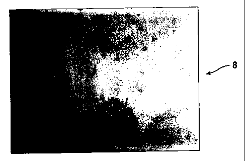
darkened"bubble-like" regions. FIG. 3 is a photomicrograph of a cross-section
of the
amorphous non-laminar nickel phosphorous alloy of the present invention as
taken by
a microscope at 500x after a 5% Nital etch wherein the Ni/P alloy 8 comprises
the
entire photomicrograph. Nickel/phosphorous alloy 8 has a plurality of faint,
diagonally
running, randomly spaced grooves which are polishing lines. The amorphous non-
laminar structure of the nickel/phosphorous alloy 8 is evident from the
absence of a
plurality of thick, parallel lines or regions.
The amorphous non-laminar structure of the alloys of the present invention
renders then particularly suitable for the fabrication of high precision
devices formed
by hard-tool turning applications. Because the alloys are amorphous non-
laminar, the
quality of the alloy deposit is consistent throughout the deposit. Hence,
there is no
tendency for the formation of "banding" or demarcation lines after hard-tool
turning.
In addition, the high phosphorous content of the alloys of the present
invention also
makes them particularly well-suited to hard-tool turning applications, with
the alloys of
the present invention having a phosphorous content of between about 13% and
about 15% being particularly preferred, and those having a phosphorous content
of
between about 16% and about 20% being especially preferred. Further, the
alloys of
the present invention, being amorphous in structure (i.e., no crystalline or
grain
structure discernible at 150,000X), are particularly well-suited to hard-tool
turning in
that the required surface finish is more easily obtained than with a non-
amorphous
metal or metal alloy, such as aluminum, copper, and stainless steels.
In addition, the amorphous non-laminar nickel/phosphorous alloys, amorphous
non-laminar nickel/cobalt/phosphorous alloys, or amorphous non-laminar
cobalt/phosphorous alloys of the present invention exhibit very low internal
stress.
This very low internal stress makes them particularly well suited to forming
articles
CA 02306819 2000-04-05
WO 99/20807 PCT/US98/22221
-22-
and/or devices, including high precision devices by the technique of
electroplating a
suitably-dimensioned load-bearing substrate mandrel and then separating the
alloy
from the substrate mandrel to form the article and/or device. The amorphous
non-
laminar nickel/phosphorous alloys, cobalt/phosphorous alloys, or
nickel/cobalt/phosphorous alloys of the present invention, because they have a
very
low internal stress, may be separated from the substrate mandrel without
distortion.
Further, the amorphous non-laminar nickel phosphorous alloys, amorphous
non-laminar nickel cobalt phosphorous alloys, and amorphous non-laminar cobalt
phosphorous alloys of the present invention are useful in resurfacing or
repairing
metal surfaces. After any necessary surface-treatment steps (e.g., machining
away
the damaged areas on the metal surface to be repaired), at least a portion of
the
damaged surface is electroplated with an amorphous non-laminar nickel
phosphorous
alloy, amorphous non-laminar nickel cobalt phosphorous alloy, or amorphous non-
laminar cobalt phosphorous alloy of the present invention using techniques and
procedures described previously. If necessary, the electoplated alloy may then
be
machined or subjected to high precision tooling as described previously. The
amorphous non-laminar nickel phosphorous alloys, amorphous non-laminar nickel
cobalt phosphorous alloys, and amorphous non-laminar cobalt phosphorous alloys
of
the present invention may be used to repair any metal or metal alloy surface.
Repairs to damaged metal surfaces made with the amorphous non-laminar
nickel phosphorous alloys, amorphous non-laminar nickel cobalt phosphorous
alloys,
and amorphous non-laminar cobalt phosphorous alloys of the present invention
are
superior to traditional metal-surface repairing techniques. Because the alloys
of the
present invention are more dense, more pure, and more defect-free than
traditional
repairing materials (e.g., inserts, welds, and plating), the repair is
virtually defect-free,
exhibiting few pits and/or inclusions. In addition, because the alloys of the
present
invention are particularly well-suited to hard tool turning, the repaired
article may be
hard tool turned to a superior mirror finish without the need for polishing
steps before
and after the plating steps. In addition, unlike repairs made with hard
chrome, repairs
made with the alloys of the present invention may be finished by remachining
CA 02306819 2000-04-05
WO 99/20807 PCT/US98/22221
-23-
techniques rather than time-consuming regrinding techniques.
Further, the amorphous non-laminar nickel/phosphorous alloys, amorphous
non-laminar nickel/cobalt/phosphorous alloys, or amorphous non-laminar
cobalt/phosphorous alloys of the present invention may be deposited at a speed
of
about 0.001" per hour, making them particularly well-suited for commercial
use. In
addition, because the time required to deposit the alloys to the required
thickness is
shortened, particulate matter is easily kept out of the electroplating
solution and the
resulting alloys exhibit increased purity over alloys formed by slow
deposition speeds.
In addition, the electroplating baths used to form the amorphous non-laminar
nickel/phosphorous alloys, amorphous non-laminar nickel/cobalt/phosphorous
alloys,
and amorphous non-laminar cobalt/phosphorous alloys of the present invention
are
viable over an extended period of time by simply replenishing reagents as
required.
Finally, although particularly well-suited for the fabrication of article
and/or
devices, including molds, molding inserts, and high precision devices, and for
the
repairing of metal surfaces, the alloys of the present invention are also
suitable for
such conventional purposes as decorative and protective purposes and for any
purpose wherein a property and/or combination of properties exhibited by the
alloys
of the present invention is required or desired.
The following examples present typical applications as described above.
These examples are understood to be illustrative only and are not intended to
limit
the scope of the present invention in any way.
Example 1
A 3" diameter aluminum disc was immersed in the an electrolytic bath
consisting of 0.5-1.5M nickel as metal; 1.5-4.OM phosphorous acid, 0.2-4.OM
phosphoric acid and 1.5-3.OM chloride and electrolytically connected to a DC
power
supply as the cathode. It was plated at a current density of 50 amps/ft2 for
10 hours.
The test part had a coating thickness of approximately 0.011". Diamond turning
gave
an excellent finish when measured with a Zygo and Wyko surface and height
measuring interferometers. In addition, a witness coupon plated under the same
conditions had a phosphorous content of 13%.
CA 02306819 2000-04-05
WO 99/20807 PCT/US98/22221
-24-
Example 2
A cylinder with dimensions of 19" long by 6" diameter was prepared with a
standard pretreament cycle, flashed with approximately 0.0005" of a standard
electroless nickel deposit, then immersed as the cathode in the solution
described in
Example 1 at a current density of 50 amps/ft2 for approximately 20 hrs. The
cylinder
was coated with 0.020" of the electrolytic nickel/phosphorous deposit. The
nickel/phosphorous electroplating solution was composed of about 0.8 to about
1.2M
nickel as metal and about 2.8 to about 3.2M phosphorous acid, and about 1.8 to
about 2-2M chloride ion. This deposit was then diamond turned with a certain
groove
geometry spanning approximately 600 miles with excellent quality and minimal
degradation of the diamond tool. For comparison, this was also attempted using
a
conventional electroless nickel deposit and the diamond tool and/or coating
quality
was unacceptable after approximately 60 miles.
Example 3
A stainless steel substrate that was approximately .375" dia. X 1.5" long was
coated with 0.050" to 0.060" of the electrolytic nickel/phosphorous deposit on
the face
of the 0.375" dia. The nickel/phosphorous electroplating solution was composed
of
about1.OM nickel as metal and about 3.OM phosphorous acid, and about 2.OM
chloride ion. A Fresnel lens with a groove depth of 0.035" was cut into the
deposit.
The quality of the final product was excellent and this was also unattainable
with
conventional electroless technology.
Example 4
An article made of a carbon/epoxy composite needed to have a highly
reflective finish on one critical surface. The composite material was chosen
for its
rigidity and light weight. The non-critical surfaces were masked. Then a
conductive
metal containing paint was sprayed on the primary surface and allowed to cure.
This
CA 02306819 2000-04-05
WO 99/20807 PCT/US9812221
-25-
rendered the surface conductive and allowed for a standard pretreatment cycle
and
subsequent electroplating in the solution described in Example 1. A high
quality
amorphous 13% nickel/phosphorous coating (by witness coupon) was obtained and
subsequently diamond turned.
Example 5
An approximately 3" diameter copper insert was coated with 0.030" of a
nickel/phosphorous alloy deposited from the solution described in Example
I.The
surface was then diamond turned with the structure needed and used as a mold
for
bi-focal eye glass lens.
Example 6
A 3" diameter piece of optical glass was masked on one side. The opposite
side was metallized using conventional pretreatment methods used in the
"plating on
plastics" industry involving seeding the glass layer with palladium and then
depositing
a thin film of electroless nickel as an electroplate base. That surface was
then built
up with a very heavy layer of the electrolytic nickel/phosphorous deposit
(0.150").
The deposit itself was then separated from the glass mandrel. The initial
layer of the
deposit formed is an exact replica of the optical glass and that surface then
becomes
the surface for molding and the remaining deposit is used for support and
rigidity.
Example 7
Two 18" diameter by 60" long mold steel rolls were coated with 0.20" of an
electrolytic nickel phosphorous alloy essentially as described in Example 1
using an
electrolytic bath consisting of 1.OM nickel as metal; 1.8 M chloride; 2.5 M
phosphorous acid; and 1.25 M phosphoric acid having a surface tension of <30
dynes/cm at a solution temperature of 160 F, cathode efficiency of 5.4 mg/amp.
min.,
current density of 25 am/s/square ft, and a deposit stress of 1500 lbs
compressive.
CA 02306819 2000-04-05
WO 99/20807 PCT/US98/22221
-26-
The deposit was ground to clean and then diamond turned with a groove
geometry.
The roll in this condition is often referred to as a lenticular lens cylinder
and is used in
a plastic extrusion process to manufacture plastic films with various groove
geometry's. These films are then used to alter or enhance images in the area
of
holographics, computer screens, and large projection screens.
After the cylinder was diamond turned, the shavings were returned and
analyzed for phosphorous content using ISO-4527 standard test method and found
to
be >14.5% (shavings from one roll having a phosphorous content of 14.6% and
the
other having a phosphorous content of 14.7%).