Note : Les descriptions sont présentées dans la langue officielle dans laquelle elles ont été soumises.
CA 02307669 2000-04-27--
, ~ " ~' , . , '. , . . ,
', ' ; . , , . , , ,
i: ; ,,. ,,.. ,~, ',,' ,' ,
Electrically tuneable optical filter
The invention relates to an electrically tuneable optical filter which may be
used, in particular,
s for spatially separating frequency components in an input beam of radiation,
at microwave or
optical frequencies. More particularly, the device may be used as a staring
spectrum analyser or
as a wavelength division multiplexer and demultiplexer.
There are two approaches to making a spectrum analyser. In one case, the input
signal to be
l0 analysed may be passed through a tuneable filter with is scanned through
the required frequency
range. The transmission against the frequency of transmission of the filter is
then measured to
give the spectrum. Such systems are known as scanning spectrum analysers.
Alternatively, the
input signal may be split into a number of identical, lower power signals,
each of which is then
passed through a different filter from a set of equally spaced filters. The
output powers of the
i 5 filter set give the spectrum required. Such systems are known as staring
spectrum analysers.
Conventional IZF' spectrum analysers, as used in the laboratory, are scanning
spectrum analysers.
This is because a scanning spectrum analyser can cover a wide range of
frequencies with a high
resolution and can easily be reconfigured as required. However, a scanning
spectrum analyser is
20 only useful for measuring input signals which are not changing rapidly, as
they can only "look"
at one frequency at a time. If, for example, the input signals contain fast
pulses, the scanned
spectrum analyser could easily miss pulses of some frequencies if it is not
looking at the right
frequency when the pulse arrives.
25 A staring spectrum analyser overcomes this problem. However, it is more
difficult to make than
a scanned spectrum analyser, especially if the number of frequency channels is
high. As splitters
tend to be narrow band components, it is difficult to split a broadband
electrical RF signal many
ways without severe distortion. Also, RF filters have to delay the signal by a
time proportional to
the inverse of the filter bandwidth, and this makes such components very large
and difficult to
30 make with low enough loss to achieve a resolution below around 100 MHz
using conventional
techniques.
O SAE
",
CA 02307669 2000-04-27
. ;',', , , , , . ,
2; ; ,:, ,'," ,.', ',. "' ,
Optical methods can be used to make both scanned and staring spectrum
analysers. An example
of a scanned optical spectrum analyser is a scanning Fabry Perot
interferometer, which comprises
two parallel (or confocal) plates which are moved towards and away from each
other (usually
using a sawtooth drive voltage). The output intensity plotted against time
gives the optical
spectrum ["Introduction to optical electronics", A. Yariv (Holt Reinhart and
Winston, 1976)].
A grating spectrometer is an example of an optical staring spectrum analyser.
This works by
splitting the input beam into many hundreds of beams, changing the phase of
each beam by an
amount which depends linearly on its position (using the grating) and
recombining all of the
1o phase shifted beams on an output detector array. Because of the phase
shifts, different optical
frequencies recombine in phase at different places in the detector array.
Another type of staring optical spectrum analyser is an acoustic-optic device
in which the signal
to be analysed is used to drive an acoustic-optic transducer which launches an
acoustic wave into
a transparent piezoelectric and electro-optic material (e.g. lithium niobate).
The acoustic waves
can set up refractive index waves in such materials which diffract a light
beam passing through
them by an amount directly proportional to the RF frequency. In practice, this
type of spectrum
analyser can give very high resolution, mainly because acoustic waves travel
much more slowly
than electromagnetic waves, allowing longer delays to be achieved in short
devices. However,
2o they tend to be limited to frequencies below a few GHz because of acoustic
losses.
Various optical waveguide versions of low resolution optical spectrometers
have been
demonstrated, usually for combining (multiplexing) or splitting
(demultiplexing) a number of
different wavelengths on one fibre. These are passive devices, however, rather
than active
devices, which are made by accurate lithography and design to control the
optical phase shifts.
However, lithographic inaccuracies are inevitable and this limits the
resolution which may be
achieved with such systems.
~~~;~.0 S
w CA 02307669 2000-04-27
UK 2 269 678 A is in the field of the present invention. It describes an
interferometric tuneable
filter formed on a semiconductor substrate on which a waveguide is split into
a plurality of
branches of equal length. Each branch has electrically controllable amplitude
and phase control
elements for modulating the amplitude and phase of light transmitted through
the branches. The
filter has the function of selecting a predetermined wavelength light signal
from a plurality of
multiplexed light signals. The light transmitted through each branch is
recombined to provide a
single device output. The device described in tIK 2 269 678 A therefore has
the disadvantage
that only one wavelength is output from the device, the others being lost in
the substrate. The
1 o device is therefore not suitable for use as a spectrum analyser or in
applications where multiple
outputs of different wavelength are required.
20
30
~r,~E~~=p SHEET
~
CA 02307669 2000-04-27
,. . .. " ..
, , , , . , , . , ,
' , , ~ , . ,
4~ . , , . . . . , . , , , , , , , ,
According to the present invention, a device for spatially separating
components of frequency in
a primary radiation beam comprises;
means for separating the primary radiation beam into a plurality of secondary
radiation beams
each having a phase, ~,
a plurality of electrically biasable waveguides forming a waveguide array,
each for transmitting a
secondary radiation beam to an output, wherein each waveguide has an
associated optical delay
line having a corresponding optical delay time, wherein each of the optical
delay times is
i o different,
means for applying a variable electric field across each of the waveguides
such that the phase, ~,
of the secondary radiation beams transmitted through each of the waveguides
may be varied by
varying the electric field,
whereby the secondary radiation beams output from each of the waveguides
interfere in a
propagation region with a secondary radiation beam output from at least one of
the other
waveguides to form an interference pattern comprising one or more maximum at
various
positions in the propagation region.
ZO
Preferably, the device provides at least two outputs.
The device may also comprise means for applying RF modulation to the primary
radiation beam.
The device may therefore be used as an optical staring spectrum analyser or an
RF spectrum
analyser and has an advantage over scanning spectrum analysers where signals
of some
frequencies may be missed if the device is not scanning at the right frequency
when a pulse of
radiation arrives. Furthermore, the device can be used to scan both optical
and microwave
frequencies by use of the RF modulation means and may be actively controlled
in use by varying
the electric fields applied across one or more of the electrically biasable
waveguides. Because the
3o phase of radiation transmitted through each of the waveguides may be
varied, any inaccuracies in
the design may therefore be corrected for in use, by varying the applied
electric fields. This
provides an advantage over passive devices used for multiplexing and
demultiplexing beams.
.,~,r~ ~~~
v,,~~f
CA 02307669 2000-04-27
" , " " ,
, ~ , ' ,
In a preferred embodiment, each adjacent pair of waveguide outputs are spaced
apart by an
amount proportional to the optical time delay difference between the
corresponding adjacent pair
of waveguides. This has the advantage that different intensity maxima
corresponding to different
optical frequencies occur at well defined angles in the propagation region and
the angular
difference between the maxima for two different frequency components is
substantially
proportional to the difference in frequency between the two frequency
components.
to In a further preferred embodiment, the waveguides may have a substantially
linear variation in
optical time delay across the waveguide array.
Typically, the optical time delay difference across the waveguide array is at
least 100
picoseconds and may be at least 10 nanoseconds.
The propagation region may be a region of free space or may be a slab
waveguide. A slab
waveguide may be used to advantage as it confines the secondary radiation
beams, for example
to a chip.
2o The electrically biasable waveguides may be group III-V semiconductor
waveguides. For
example, GaAs or InP/InGaAsP waveguides may be used.
The electrically biasable waveguides may be formed in one with the optical
delay lines and the
device may be formed on a single chip. Alternatively, each of the electrically
biasable
waveguides may comprise a electrically biasable waveguide and an optical fibre
delay length.
The means for separating the primary radiation beam into a plurality of
secondary radiation
beams is a mufti mode interference splitter.
3o Each of the electrically biasable waveguides may have independent means for
varying the
electric field across the electrically biasable waveguide portion. For
example, each electrically
biasable waveguide may have an independent variable voltage supply.
;. -.L
~~as3:.-.u'us:~~:_4, iv~.i~~
~
. CA 02307669 2000-04-27
" , , , , . ,
' ; ; ~~ , , . , , '.,' " .
, , ,
' ~ , , , , ,. , , ~ ~ r ~ ~ , v
a
The device may also comprise one or more output waveguide located within the
propagation
region, such that the or each output waveguide may receive a secondary
radiation beam of
selected frequency output from one or more waveguide.
In addition, or alternatively, the device may also comprise an input laser
having a laser cavity,
wherein the electrically biasable waveguities form part of the laser cavity to
enable selective
wavelength tuning of the laser by variation of the electric fields applied
across each of the
waveguides.
According to a second aspect of the invention, a method for spatially
separating components of
frequency in a primary radiation beam comprises the steps of;
(i) separating the primary radiation beam into a plurality of secondary
radiation beams each
having a phase, ~,
(ii) transmitting each of the secondary radiation beams through one of a
plurality of electrically
biasable waveguide forming a waveguide array, wherein each waveguide has an
associated
optical delay line having a corresponding optical delay time, wherein each of
the optical delay
2o times is different,
(iii) applying a variable electric field across each of the electrically
biasable waveguides and
(iv) varying the electric field across each of the electrically biasable
waveguides so that the
phase, ~, of the secondary radiation beams transmitted through each of the
electrically biasable
waveguides may be varied,
(v) outputting the secondary radiation beams into a propagation region within
which they may
interfere with one or more of the other secondary radiation beams and
(v) forming an interference pattern in the propagation region comprising one
or more maximum
at various positions.
y ::''':~: a
v-.. ,
CA 02307669 2000-04-27
. ; , , , , , . , " . '
' ; ; ,' , ; ,
7; , ", ,;,. ", ',.~ ,,
The method may comprise the further step of;
(vi) deducing the frequency components in the primary input beam from the
positions of the or
each maximum in the propagation region.
15
25
CA 02307669 2000-04-27
8. ; , , .", ", "~ . ,
The invention will now be described, by example only, with reference to the
following figures in
which,
Figure 1 shows a schematic perspective view of a known electro-optic waveguide
device,
Figure 2 shows a schematic diagram of the invention,
Figure 3 shows a mask diagram of a single chip GaAs waveguide array device
having a variable
optical delay across the array,
Figure 4(a) shows an infrared camera photograph of the far field diffraction
pattern obtained
from the electro-optic waveguide device shown in Figure 3 for an input laser
beam without any
input modulation,
Figures 4(b) and 4(c) show infiared camera photographs of the far field
diffraction pattern
obtained from the electro-optic waveguide device shown in Figure 3 for an
input laser beam with
RF modulation,
2o Figure 5 shows line scans of the far field diffraction pattern for an input
laser beam with no input
modulation, showing the effect of changing the input laser wavelength,
Figure 6 shows line scans of the far field intensity pattern with the
unmodulated input beam
nulled and the modulation sidebands, present for three different frequencies
and
30
Figure 7 shows the line scans shown in Figure 6 on an expanded scale, to
remove the effects of
diffraction sidebands.
AMENDED SHEd'~
.- - ~ CA 02307669 2000-04-27
g; ; .;, ,;" ", '"' ~. ,
A part of an electro-optic waveguide device which may be used in the invention
is shown in
Figure 1. The electro-optic waveguide device and its operation is described in
US patent 5 239
598. In summary, the device, referred to generally as 1, comprises a heavily
doped n-type (n+)
GaAs substrate 2 typically having a doping concentration of 1 x 10'g crri 3.
This layer 2 is
overlaid with a cladding layer 3 of n+ Ga,~AI,.xAs with like dopant species
and concentration.
The cladding layer 3 is surmounted by a waveguide core layer 4. This layer 4
is composed of ri
(undoped, residual n-type) GaAs. The layers may be considered as being all of
the GaxAl,.xAs
1o system. The layer 4 has grooves 5 extending into its upper surface 6,
extending from the front
face of the device 1 most but not all of the way to a parallel rear face (not
shown) having
horizontal and vertical edges (7, 8 respectively). Rib waveguides 9 are
defined between the
grooves 5. Typically, the waveguides 9 have a width of 2.6 p,m and a length of
3 mm. Figure 1
illustrates two waveguides 9 (three grooves 5), although in practice a much
greater number of
waveguides will be included in the complete device.
Each of the waveguides 9 is coated with a layer of aluminium 10 and bond pad
11 connected to a
DC bias voltage source 12. Each waveguide 9 is therefore individually
addressed. The front face
13 and the rear face 7/8 of the device 1 are carefully cleaved to provide
optical quality surfaces.
In operation, the device 1 may be illuminated with radiation (represented by
line 20) focused to a
small spot (say, 2 ~.m diameter) on the waveguide layer 4 region of the rear
face 7/8. Typically,
this is 500 ~,m from the waveguide ends. The light then diverges from the spot
to the waveguides
9. Light beams emerging from the waveguides 9 are indicated by divergent
arrows such as 21.
The emergent light beams 21 combine to form a common far field diffraction
pattern having a
central intensity maximum 22, at position 24, and two or more subsidiary
maximum 23, as
illustrated at the bottom of Figure 1.
O~O S~~G~
f
,,~,ArN
CA 02307669 2000-04-27
, " , " , . ,
10~ , , , ~", ,;, ~"' ,'
Each waveguide 9 may support horizontal and vertical modes of light
propagation. The
waveguides 9 produce light output intensity substantially confined to the
lowest order horizontal
and vertical modes and the output of higher order horizontal and vertical
modes is inhibited. The
result is that the waveguides 9 in combination produce a far field diffraction
pattern arising
substantially from lowest order spatial modes. For further explanation of the
behaviour of light
propagating through the device, see US 5 239 598.
The refractive index and optical path length on each waveguide 9 are dependent
on the electric
field supplied by means of voltage supply 12, since the waveguide core layer
material 4 has
to electro-optic (i.c. electro-refractive) properties. Variation of the
voltage on the aluminium layer
of any waveguide 9 consequently alters the phase of its light output. The far
field diffraction
pattern is a vector sum of phase and amplitude contributions from the
waveguides 9 and the
position of the principal maximum 24 may be varied by varying the waveguide
voltages. By
controlling the voltages applied to the electrodes on each of the waveguides,
the beam in the far
t 5 field diffraction pattern can therefore be formed and scanned, or focused
electronically. The far
field diffraction pattern produced by the device 1 is fully formed at a range
of less than 0.5 mm
in air, or less than 1.8 mm in a GaAs medium. Beam steering through up to
20° may be achieved
with waveguide voltages in the region of 20 V.
The present invention is a device for spatially separating components of
different frequency in an
input beam of radiation and comprises an array of electro-optic waveguides
with each waveguide
having an associated optical delay line of different optical delay. Typically,
the electro-optic
waveguides have the construction of the electro optic waveguide array shown in
Figure 1, with
an additional upper cladding layer of ri GaxAl,_xAs (1 x 10'5 cni3) to reduce
optical losses by
keeping the light away from the electrode metal. In the conventional device
shown in Figure 1
the far field beam may be steered by varying the voltages applied to each
individual waveguide.
Hence, the far field diffraction pattern may be electronically steerable. In
the present invention,
the far field diffraction pattern is frequency steerable as well as
electronically steerable due to the
different delay lengths of each waveguide. Therefore, if the delay lengths are
short, for example
3o 500 ~,m, the device may be used as an optical spectrum analyser and if the
delay lines are long,
for example 10 cm , the device may be used as a microwave spectrum analyser.
r,
r,~t~ S~'
- CA 02307669 2000-04-27
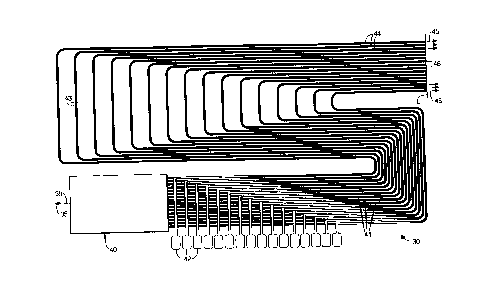
14 ~ ,:, ".~ .~. '..~ " ,.
A schematic diagram of one embodiment of the device 30 of the present
invention is shown in
Figure 2. The apparatus comprises an n-way splitting device 31 and n optical
phase shifters 32.
For example, the optical phase shifters 32 may be the electro-optic waveguide
device 1 shown in
Figure 1. The device 30 also comprises an array of n optical delay lines 33,
having a linear
variation in delay length across the array, and an output linear phased array
34. The output
spectrum from the device 30 may be viewed on a TV camera or a staring linear
detector array 37
to record, process, display or store the output spectrum. A beam of radiation
35 to be scanned
may be input to the device 30 directly. Alternatively, the beam 35 may be
modulated by an
electro-optic intensity modulator 36. The function of the electro-optic
intensity modulator 36 will
to be described in more detail later.
In one embodiment of the invention, the device 30, represented schematically
in Figure 2, may
be formed on a single chip. By way of example of a single chip device, there
now follows a
description of a 16 waveguide, single chip GaAs device.
A mask diagram of a single chip 16 channel GaAs electro-optic waveguide device
is shown in
Figure 3. The device 30 comprises an input waveguide 39, into the beam 35 is
input, and a 1 to
16 way multimode interference splitter 40 for splitting the input beam 35 into
n different outputs.
For example, this may be a multimode interference splitter as described in US
patent 5 410 625.
2o The device 30 also comprises 16 electro-optic waveguides 41 for optical
phase control, each
electro-optic waveguide 41 having an electrode 42 for applying an electric
field across each
waveguide 41. This enables each waveguide 41 to be individually addressed.
Associated with each electro-optic waveguide 41 is an optical delay line 43,
each being of a
different length. Preferably, there is a substantially linear variation in
delay length across the
electro-optic waveguide array. At the output of the delay lines 43 is a
closely spaced output
waveguide array 44. The output waveguide array is illustrated in the figure as
an array of
horizontal black lines 44, each having an output position 46, in connection
with the delay lines
43.
r,t~,R=.~~~~~ S~v~~
CA 02307669 2000-04-27
la~ ~ , ; , , , , , , ; , ~ , , ~ . , ,
In practice, and for ease of construction, each electro-optic waveguide 41,
the associated delay
line 43 and the associated output waveguide 44 may be formed as one waveguide
such that the
device is an array of electro-optic waveguides each having a different length
(i.e. having a
different delay). An array of elector-optic waveguides each having a different
optical length shall
herein be referred to as an array of electro-optic waveguide delay lines. It
is also possible to
construct the device such that the components 41,43 and 44 are separated on a
single chip.
Typically, the electro-optic waveguides 41 have the form of the structure
shown in Figure 1 and
are represented in the figure as horizontal black lines extending from the
optical sputter 40.
1o In use, continuous wave radiation 35 from an input laser (not shown) rnay
be input to the device
30 at the multimode interference splitter 40, where the input beam is split
into 16 channels. Each
of the 16 split signals is passed through one of the electro-optic waveguides
41 (or phase
shifters), into the associated delay line 43 and then to the output waveguides
44 forming an
output waveguide array. A set of 16 output beams 45 therefore emerge from the
output
waveguides 44, at positions 46, into a region in which they interfere, herein
referred to as the
propagation region. Typically, the propagation region may be a slab waveguide
(not shown) such
that the emerging beams 45 are confined on the chip, but propagate as if in
free space.
Alternatively, the propagation region may be a region of free space.
2o The output beams 45 from each of the output waveguides 44, output at
positions 46, interfere in
the propagation region with most or all of the output beams 45 from the other
output waveguides
44 such that different frequency components form intensity maxima at different
positions within
the propagation region. The interference pattern, or far field diffraction
pattern, typically at a
distance of a few millimetres or so, may then be viewed using a camera
sensitive to the particular
wavelength of light.
.'~-1 s ~:;YY
' ~ CA 02307669 2000-04-27
13 ; ,.. .;,~ .;, '.,' .,' ,
The output waveguides 44 are closely spaced, typically with a spacing of less
than 100 ~,m, and
preferably more closely spaced e.g. between 5-20 pm separation between
adjacent output
positions 46. The output positions 46 of each output waveguide 44 are arranged
to be along a
substantially rectilinear line, L. Preferably, the output waveguides 44 are
spaced such that the
centre-to-centre pitch between any two adjacent output positions 46 is
directly proportional to the
optical time delay difference between those two adjacent output waveguides.
This ensures
intensity maxima corresponding to different optical frequencies will occur at
well defined angles
in the propagation region and that the angular difference between the maxima
for two different
frequency optical beams will be directly proportional to the difference in
frequency between the
to two beams.
In a further preferred embodiment, the output positions 46 are spaced equally
and have the
corresponding optical time delay differences between each pair of adjacent
waveguide delay
lines also correspondingly equally spaced, such that the optical delay lines
43 have a
substantially linear variation in delay length across the array. Typically,
this may correspond to a
spread of time delays between 0 and 1 nanosecond (i.e. the relative delay of
the n'" waveguide is
n/16 nanoseconds, where n=1 to 16). In this embodiment, the device 30 may be
operated as a 16
channel spectrum analyser having a 1 GHz channel separation. If the optical
time delay
difference between adjacent delay lines is of the order of 100 ps, this gives
a free spectral range
(i.e. the maximum frequency range of operation) of 10 GHz, and a resolution of
10 GHz / N,
where N is the number of delay lines. The difference between the maximum and
minimum delay
line lengths therefore determines the frequency resolution which may be
achieved with the
device.
Results have been obtained for a device having the form of the GaAs chip
device shown in
Figure 3 for an input diode pumped Nd:YAG laser beam at 1.064 ~,m. If the
voltages applied to
the electro-optic waveguides 41 are initially set so that all of the 16 output
beams 45 are in phase,
this gives a single main beam in the far field diffraction pattern and two
sidelobes (due to the
periodicity of the output intensity pattern). This is illustrated in Figure
4(a) which shows a single
3o main beam 47a and two sidelobes 47b. The main beam 47a and sidelobes 47b
may then be
scanned by changing the phase of the 16 output beams linearly across the
array.
-,~_;,
CA 02307669 2000-04-27
14~ ; , ' , , ' , , ; , ' , , , ,
For example, if the phases were stepped (from the uniform starting condition)
by 360°/16 (i.e.
22.5°) across the array, the beam would steer by 1/l6th of the main
beam-to-first sidelobe
separation distance. More generally, if the phases were stepped by n x
22.5°, the beam would
steer by n/l6th of the main beam-to-first sidelobe separation distance until,
when n=16, the
original pattern would be reproduced as the array output beams would be in
phase again (as in
the initial condition).
In practice, the phases could always be set to values within the range 0 to
360° by suitable choice
i o of the voltages applied to the electrode of each waveguide. The effect of
using added delay lines,
rather than equal length waveguides, is that the beam may also be steered if
the input optical
wavelength or frequency is altered. This cannot be achieved with a
conventional electro-optic
waveguide but is possible in the present device because, as the input
wavelength is changed, the
output phases change linearly across the array, in the same way as for the
main beam being
electronically scanned. For example, for a device with a linear 0 to 1
nanosecond waveguide
delay line set, a 1 GHz frequency change of the input optical beams steers the
beam through
1/l6th of the main beam-to first sidelobe separation, because a change of the
optical frequency of
1 GHz corresponds to a change of exactly one cycle per nanosecond, or a
360° phase shift in a 1
nanosecond delay line.
The delay of the n~ waveguide gives a corresponding phase shift of n x
22.5°, which is the
required set of phases for steering the beam through 1/l6th of the main beam-
to-first sidelobe
separation. Thus, the device provides frequency dependent beam scanning which
has many
advantages over electronic scanning. Furthermore, the two types of scanning
implemented
together give the device still further advantages. Although the device is
described as a 16 channel
device, a smaller or greater number of channels may be used in practice.
_...~~-, s'ri
w ~ ' CA 02307669 2000-04-27
15~ ~ , ; , , . . , ' , ~ . , '
A particularly useful application of the device is as a staring spectrum
analyser. The device may
be operated as an optical spectrum analyser or an RF spectrum analyser.
Referring to Figure 2,
for RF spectrum analysis, the input beam of radiation 20 to be analysed is
passed through an
electro-optic frequency modulator 36 before entering the device 30. A
microwave signal 50
applied to the modulator 36 therefore adds frequency components to the input
wave 20 which are
deflected through different angles (proportional to the modulation frequency)
by the delay line
phased array 41/43.
It is important to use a balanced electro-optic modulator 36 to avoid adding
higher harmonics
1 o and to allow the frequency of the input beam to be removed from the far
field diffraction pattern.
By setting the intensity modulator to a null, the input beam may be suppressed
to show only the
modulation sidebands. This is illustrated in the spectra shown in Figures 4(b)
and 4(c) in which
the frequency of the input beam has been removed from the spectra.
Figure 5 shows the intensity of the output waveguide array as a fimction of
distance across the
far field diffraction pattern for an input laser at three different
frequencies (curves 48,49,50). This
illustrates the added effect of using delay lines in combination with the
electro-optic waveguides.
That is, the beam may be steered if the input optical wavelength or frequency
is changed, as well
as by varying the voltages applied to the waveguides.
Figure 6 shows the intensity scan of the far field diffraction pattern for
three different RF
frequencies, 2 GHz, 3 GHz, and 5 GHz, (curves 51,52,53 respectively) with the
intensity
modulator 36 set to null. The carrier beam is suppressed and only the
modulation sidebands are
present in the scan. Figure 7 shows the intensity scans shown in Figure 6 on
an expanded scale
(arbitrary units), with the intensity scan for no modulation signal (peak 54)
also shown. If a
number of different frequencies are used to modulate the input beam, they will
all be observed
simultaneously in the diffraction pattern. The device does not therefore scan
through the
frequency range as in a conventional scanning spectrum analyser.
..-,
. .~ ~~! y'L~''.
~.
.~'v.ul~' ov
" ' CA 02307669 2000-04-27
16~ ~ , ; , . ~ ~ , , : , ' . . ' , ~ '
Without the optical modulator 36 in Figure 2, the device essentially operates
as an electrically
tuneable optical spectrometer. It is capable of delivering an arbitrarily high
optical resolution
which is better than that which may be achieved using conventional optical
grating
spectrometers, the resolving power of which is limited by the grating width
and pitch. The
performance also matches that of scanning Fabry-Perot etalon interferometric
spectrometers but
has the advantage of being able to analyse optical spectra with an arbitrary
number of output
channels, each of which is staring and does not require scanning to measure
the spectrum.
Another application of the device is as an electrically controllable
wavelength division
1 o multiplexer/demultiplexer. This is of particular use in the field of
optical fibre
telecommurucations. Wavelength division multiplexing/demultiplexing is used to
combine a
number of closely spaced wavelength laser beams on to an optical fibre, and to
separate them at
the other end. In conventional wavelength division
multiplexers/demultiplexers, this is achieved
passively which means that the device must be constructed with high accuracy
in order to set to
the required frequency [Y. moue, Integrated Photonic Research 1996, Conference
Proceedings,
April 1996, Boston USA, Paper IMC1 pp 32-35, C. van Dam et al., Integrated
Photonics
Research 1996, Conference Proceedings, April 1996, Boston USA, Paper IMC6 pp
52-55].
The present device may be as a wavelength division multiplexer/demultiplexer
and provides an
2o advantage over known multiplexers in that active alignment is possible by
fine tuning the
voltages applied to the electrodes on the electro-optic waveguides. Active
control of the centre
wavelength, and fme control of the individual waveguide phase shifts, are
important in
wavelength division multiplexing as, in practice, it is difficult to make
passive devices with
sufficient accuracy.
In practice, in wavelength division multiplexing/demultiplexing, the frequency
separation does
not need to be too large, typically around 50-100 GHz, as opposed to the
typical values of
around 1 GHz required in a spectrum analyser. This means that the optical
delay lengths need not
be as long as in the spectrum analyser application. For a 100 GHz resolution,
for example, the
3o difference between the maximum and minimum delay lengths would be 800 Vim.
,,
. r;.~~; ~ .
CA 02307669 2000-04-27
li' , , , ~ ~ , , ,
The device may also be used to control the wavelength of an on-chip laser.
Versions of such
devices which use an array of passive waveguide delays are described by M.
Zirngibl et al.,
Integrated Photonics Research 1996, Conference proceedings, April 1996, Boston
USA, Paper
IMC6 pp 52-55 and L.H. Spiekman et al., Integrated Photonics Research 1996,
Conference
proceedings, April 1996, Boston USA, Paper IMC3 pp 136-139. However, these
devices are
difficult to design and construct accurately enough to set the wavelength to
any required value.
In the present case, the array may be used as part of the laser cavity to act
as a wavelength filter.
For example, referring to Figure 3, a gain region may be placed in the input
waveguide 60,
1 o situated before the n-way splitter 40 and a reflector (not shown) may be
placed in the propagation
region. The reflector is arranged so that it only reflects light of one
particular frequency back into
the array of delay lines 43, so that the cavity gain is maximum for the chosen
frequency, and the
device therefore lases at a wavelength corresponding to the reflected optical
frequency providing
the cavity gain is high enough. By using an away of electrically tuneable
device of the present
invention, rather than a passive array, the laser frequency may be set
accurately to any required
value to an accuracy within the resolution limits of the array. Typically,
this may be <100 MHz.
The laser wavelength may be held constant or tuned electronically by adjusting
the voltages
applied to the electrodes on the electro-optic waveguides, thus providing
feedback into the laser
cavity only at one wavelength. This device may be of particular use for the
generation of
2o microwave frequencies which requires fine tuning of two input laser
frequencies.
The embodiment of the invention shown in Figure 3 is described for a single
chip GaAs device.
Although in practice it may be more convenient to fabricate the device on a
single chip,
alternatively the delay line array could be deployed on a separate chip from
the electrically
biasable waveguide array. Other III-V semiconductor waveguide technology may
also be used,
for example InP/InGaAsP.
.~i i-.:.1
CA 02307669 2000-04-27
, ~ , " , , ,
18~ ; ~ ~ , , , , , . , , , .
In another embodiment of the invention, the device may be a fibre based device
in which the
electro-optic waveguides are used in combination with fibre based components.
For example,
referring to Figure 2, the optical delay lines 32 may be optical fibres of
different length.
Similarly the n-way splitter 31 may a fibre component or a glass block. If
optical fibres are used
it may be preferable to have electro-optic waveguides formed on a lithium
niobate chip, rather
than a GaAs chip.
With reference to Figure 2, the device is arranged such that the split input
beams pass through
the electrically biasable waveguides before passing through the delay lines
33. However, the
1 o device may also be configured such that sequence in which the phase
control and delay functions
are implemented is reversed so that the delay function is introduced prior to
the phase control.
For example, in a fibre based device, this may be achieved by having optical
fibre delay lines 33
situated between the n-way splitter 31 and the electrically biasable
waveguides 32. Similarly,
referring to Figure 3, for a single chip device, the varying delay lengths 43
may be situated
before the electrodes 42 for implementing the phase control.
The input laser, from which the input beam is generated, the electro-optic
modulator and the n-
way splitter and phase shift array may all be employed on a single chip. This
enables a small,
light and rugged device to be constructed, with the dimensions depending only
marginally on
2o the number of channels required.
The device can be easily operated over a wide spectral range, limited by the
transparency of the
electro-optic material and also any external delay line medium. Current GaAIAs
technology
enables coverage of the wavelength range between 0.7 ~,m and 10 Vim. The
device also has the
ability to perform RF spectrum analysis, when used with an optical modulator
device at the
input.
NQ~~ S~'E
AMA
-w ~w ' CA 02307669 2000-04-27
19~ ; ,;, .:,~ ,;, ',,' ,,'
If the device is used with a tuneable CW laser beam as the input, it will
electronically scan, as
well as scanning in small changes in wavelength, without any adjustment of the
phase shifters
used in the device. Furthermore, if linear arrays are connected to output
fibres and these fibres
are brought into a two dimensional array, an x-y scanning ability may be
achieved by arranging
short delays between each linear array input. The linear arrays would need to
have a very high
wavelength sensitivity (using long delays) so that when the free spectral
range (or planned
scanned angle) is exceeded, the next scan is displaced a small amount normal
to the first scan
axis.
to
20
30
. w PC~O~~ SHEE