Sélection de la langue

Search

Sommaire du brevet 2309436 

Énoncé de désistement de responsabilité concernant l'information provenant de tiers

Une partie des informations de ce site Web a été fournie par des sources externes. Le gouvernement du Canada n'assume aucune responsabilité concernant la précision, l'actualité ou la fiabilité des informations fournies par les sources externes. Les utilisateurs qui désirent employer cette information devraient consulter directement la source des informations. Le contenu fourni par les sources externes n'est pas assujetti aux exigences sur les langues officielles, la protection des renseignements personnels et l'accessibilité.

Disponibilité de l'Abrégé et des Revendications

L'apparition de différences dans le texte et l'image des Revendications et de l'Abrégé dépend du moment auquel le document est publié. Les textes des Revendications et de l'Abrégé sont affichés :

  • lorsque la demande peut être examinée par le public;
  • lorsque le brevet est émis (délivrance).
(12) Brevet: (11) CA 2309436
(54) Titre français: DISPOSITIF DE COMMANDE DE LA LONGUEUR D'ONDE D'UN LASER
(54) Titre anglais: LASER WAVELENGTH CONTROL DEVICE
Statut: Durée expirée - au-delà du délai suivant l'octroi
Données bibliographiques
(51) Classification internationale des brevets (CIB):
  • H01S 03/13 (2006.01)
  • G02F 02/00 (2006.01)
  • H01S 05/0687 (2006.01)
(72) Inventeurs :
  • MIZRAHI, VICTOR (Etats-Unis d'Amérique)
  • HARMON, STEPHEN R. (Etats-Unis d'Amérique)
(73) Titulaires :
  • CIENA CORPORATION
(71) Demandeurs :
  • CIENA CORPORATION (Etats-Unis d'Amérique)
(74) Agent: KIRBY EADES GALE BAKER
(74) Co-agent:
(45) Délivré: 2005-11-15
(86) Date de dépôt PCT: 1998-05-08
(87) Mise à la disponibilité du public: 1998-11-12
Requête d'examen: 2003-02-05
Licence disponible: S.O.
Cédé au domaine public: S.O.
(25) Langue des documents déposés: Anglais

Traité de coopération en matière de brevets (PCT): Oui
(86) Numéro de la demande PCT: PCT/US1998/009283
(87) Numéro de publication internationale PCT: US1998009283
(85) Entrée nationale: 2000-05-02

(30) Données de priorité de la demande:
Numéro de la demande Pays / territoire Date
08/848,423 (Etats-Unis d'Amérique) 1997-05-08

Abrégés

Abrégé français

Cette invention se rapporte à un système de commande de laser comportant un microprocesseur, qui règle précisément la longueur d'onde du rayonnement émis par un laser (118) en contrôlant la transmissivité d'un réseau (124) de diffraction de Bragg en fibres couplé à la sortie du laser. Le réseau de Bragg est fabriqué de manière à posséder une transmissivité minimale pour la longueur d'onde de sortie souhaité du laser. Le microprocesseur règle en permanence la longueur d'onde de la sortie de laser de façon à ce que la transmissivité soit sensiblement minimale à travers le réseau. Le laser est alors bloqué, à ce stade, à la longueur d'onde souhaitée. Le microprocesseur peut également contrôler le rayonnement réfléchi par le réseau de diffraction, et ajuster en continu la longueur d'onde de la sortie du laser de manière à bloquer le laser à une longueur d'onde assurant une réflectance sensiblement maximale. L'invention se rapporte également à l'utilisation de ce système dans un convertisseur de longueur d'onde optoélectronique.


Abrégé anglais


A laser control system is disclosed including
a microprocessor, which precisely adjusts the
wavelength of light ouput from the laser (118)
by monitoring the transmissivity of an in-fiber
Bragg grating (124) coupled to the output of the
laser. The Bragg grating is fabricated to have
a minimum transmissivity at the desired output
wavelength of the laser. The microprocessor
continually adjusts the wavelength of the laser
output to obtain substantially minimal transmissivity
through the grating. At which point, the laser is
locked to the desired wavelength. Alternatively,
the microprocessor can monitor light reflected
from the grating, and continually adjust the
wavelength of the laser output to lock the laser at a
wavelength providing substantially maximum
reflectance by the grating. Use in an optoelectronic
wavelength converter.

Revendications

Note : Les revendications sont présentées dans la langue officielle dans laquelle elles ont été soumises.


-15-
Claims:
1. An optical device, comprising:
a first source of light, said light having a first wavelength dependent upon a
temperature of said first source;
a filtering element coupled to said first source of said light;
a first photoelectric conversion device configured to detect a portion of said
light transmitted through said filtering element and generate an electrical
sense signal in
response thereto;
a control circuit coupled to said first photoelectric conversion device;
a temperature regulating device coupled to receive a control signal generated
by
said control circuit in response to said electrical sense signal, said
temperature
regulating device adjusting a temperature of said first light source in
response to said
control signal to thereby adjust said first wavelength;
a second source of light at a second wavelength different than said first
wavelength;
a second photoelectric conversion device coupled to said second source and
generating a detection signal in response to said light at said second
wavelength for
modulating said light at said first wavelength; and
a circuit coupled to said second photoelectric conversion device, said second
photoelectric conversion device supplying said detection signal to said
circuit, said
circuit being configured to facilitate modulation of said light at said first
wavelength.
2. An optical device in accordance with claim 1, wherein said circuit
further comprising:
a modulation circuit coupled to receive said detection signal, said modulation
circuit outputting a modulation signal in accordance with said detection
signal; and

-16-
an optical modulator configured to receive said modulation signal to thereby
modulate said light at said first wavelength.
3. An optical device in accordance with claim 1, wherein said first source
of light comprises a laser.
4. An optical device in accordance with claim 1, wherein said filtering
element comprises an in-fiber Bragg grating.
5. An optical device in accordance with claim 1, wherein said filtering
element has a transmission characteristic whereby a minimum transmittance is
obtained
at a predetermined wavelength, said first wavelength being substantially equal
to said
predetermined wavelength.
6. An optical device in accordance with claim 2, wherein said optical
modulator comprises a Mach-Zehnder interferometer.
7. An optical device comprising:
a first source of light at a first wavelength, said first wavelength being
dependent upon a temperature of said first source;
a reflective element coupled to said source of said first light;
a first photoelectric conversion device configured to detect a portion of said
light reflected by said reflective element and generate an electrical sense
signal in
response thereto;
a control circuit coupled to said first photoelectric conversion device;
a temperature regulating device coupled to receive a control signal generated
by
said control circuit in response to said electrical sense signal, said
temperature
regulating device adjusting a temperature of said first light source in
response to said
control signal to thereby adjust said first wavelength;

-17-
a second source of light at a second wavelength different than said first
wavelength;
a second photoelectric conversion device coupled to said second source and
generating a detection signal in response to said light at said second
wavelength for
modulating said light at said first wavelength; and
a circuit coupled to said second photoelectric conversion device, said second
photoelectric conversion device supplying said detection signal to said
circuit, said
circuit being configured to facilitate modulation of said light at said first
wavelength.
8. An optical device in accordance with claim 7, wherein said circuit
further comprising:
a modulation circuit coupled to receive said detection signal, said modulation
circuit outputting a modulation signal in accordance with said detection
signal; and
an optical modulator configured to receive said modulation signal to modulate
said light at said first wavelength.
9. An optical device in accordance with claim 7, wherein said reflective
element comprises an in-fiber Bragg grating.
10. An optical device in accordance with claim 7, wherein said reflective
element has a reflectivity characteristic whereby a maximum reflectance is
obtained at a
predetermined wavelength, said control circuit adjusting said wavelength to be
substantially equal to said predetermined wavelength.
11. An optical device in accordance with claim 8, wherein said optical
modulator circuit comprises a Mach-Zehnder interferometer.
12. An optical device comprising:
a first source of light at a first wavelength;

-18-
a partially reflective element coupled to said first source of said light at
said first
wavelength;
a first photoelectric conversion device configured to detect a first portion
of said
light at said first wavelength transmitted through said partially reflective
element and
generating a first electrical sense signal;
a second photoelectric conversion device configured to detect a second portion
of said light at said first wavelength reflected by said partially reflective
element and
generating a second electrical sense signal;
a comparator circuit configured to receive said first and second electrical
sense
signals and generating an output signal corresponding to a comparison between
said
first and second electrical sense signals;
a control circuit coupled to said comparator circuit, said control circuit
adjusting
said first wavelength of said light in response to said output signal;
a second source of light at a second wavelength different than said first
wavelength;
a third photoelectric conversion device coupled to said second source and
generating a detection signal in response to said light at said second
wavelength; and
a circuit coupled to said second photoelectric conversion device, said second
photoelectric conversion device supplying said detection signal to said
circuit, said
circuit being configured to facilitate modulation of said light at said first
wavelength.
13. An optical device in accordance with claim 12, wherein said first source
comprises a laser.
14. An optical device in accordance with claim 12, wherein said partially
reflective element comprises an in-fiber Bragg grating.

-19-
15. An optical device in accordance with claim 12, wherein said first
wavelength of said light is dependent upon a temperature of said first source,
said
optical device further comprising:
a temperature regulating device coupled to receive a control signal generated
by
said control circuit in response to said output signal, said temperature
regulating device
adjusting a temperature of said first source in response to said control
signal to thereby
adjust said first wavelength.
16. An optical device in accordance with claim 12, wherein said circuit
comprises:
a modulation circuit coupled to receive said detection signal, said modulation
circuit outputting a modulation signal in accordance with said detection
signal; and
an optical modulator configured to receive said modulation signal to modulate
said light at said first wavelength.
17. An optical device in accordance with claim 16, wherein said optical
modulator comprises a Mach-Zehnder interferometer.
18. A method of regulating a wavelength of light output from a laser,
comprising the steps of:
transmitting said light through a partially transmissive element having a
transmission characteristic whereby a minimum transmissivity is obtained at a
predetermined wavelength;
increasing said wavelength in first increments until a transmissivity of said
light
increases at a first wavelength;
decreasing said wavelength in second increments until said transmissivity of
said light increases at a second wavelength; and

-20-
adjusting said wavelength to be a third wavelength between said first and
second wavelengths.
19. A method in accordance with claim 18, further comprising the steps of:
changing said wavelength in third increments less than said first increments
until said transmissivity of said light through said element increases at a
fourth
wavelength between said first and third wavelengths;
changing said wavelength in fourth increments less than said second increments
until said transmissivity of said light through said element increases at a
fifth
wavelength between said second and third wavelengths; and
adjusting said wavelength to be sixth wavelength between said fourth and fifth
wavelengths.
20. A method in accordance with claim 18, wherein if said first increments
are equal to a predetermined value, said method further comprising the steps
of:
changing said wavelength in said first increments until said transmissivity of
said light through said element increases at a fourth wavelength between said
first and
third wavelengths;
changing said wavelength in said second increments until said transmissivity
of
said light through said element increases at a fifth wavelength between said
second and
third wavelengths; and
adjusting said wavelength to be a sixth wavelength between said fourth and
fifth
wavelengths.
21. A method in accordance with claim 18, wherein said increasing step
further comprises the steps of:
monitoring a temperature of said laser; and

-21-
delaying successive ones of said first increments of said wavelength at least
until said temperature of said laser is substantially constant.
22. A method in accordance with claim 18, wherein said partially
transmissive element comprises an in-fiber Bragg grating, said method further
comprising the steps of:
monitoring a temperature of said in-fiber Bragg grating; and
discontinuing said increasing and decreasing steps when said temperature
exceeds a first value or falls below a second value.
23. A method in accordance with claim 18, further comprising the step of
generating an alarm signal when an intensity of said light output from said
laser
exceeds a first value or falls below a second value.
24. A method of regulating a wavelength of light output from a laser,
comprising the steps of:
reflecting said light off a partially reflective element having a reflectivity
characteristic whereby a maximum reflectivity is obtained at a predetermined
wavelength;
increasing said wavelength in first increments until a reflectivity of said
partially reflective element decreases at a first wavelength;
decreasing said wavelength in second increments until said reflectivity of
reflective element decreases at a second wavelength; and
adjusting said wavelength to be a third wavelength between said first and
second wavelengths.

-22-
25. A method in accordance with claim 24, further comprising the steps of:
changing said wavelength in third increments less than said first increments
until said reflectivity of said partially reflective element decreases at a
fourth
wavelength between said second and third wavelengths;
changing said wavelength in fourth increments less than said second increments
until said reflectivity of said partially reflective element decreases at a
fifth wavelength;
and
adjusting said wavelength to be a sixth wavelength between said fourth and
fifth
wavelengths.
26. A method in accordance with claim 24, wherein if said first increments
are equal to a predetermined value, said method further comprising the steps
of:
changing said wavelength in said first increments until said reflectivity of
said
partially reflective element decreases at a fourth wavelength;
changing said wavelength in said second increments until said reflectivity of
said partially reflective element decreases at a fifth wavelength; and
adjusting said wavelength to be a sixth wavelength between said fourth and
fifth
wavelengths.
27. A method in accordance with claim 24, wherein said increasing step
further comprises the steps of:
monitoring a temperature of said laser; and
delaying successive ones of said first increments of said wavelength at least
until said temperature of said laser is substantially constant.
28. A method in accordance with claim 24, wherein said partially reflective
element comprises an in-fiber Bragg grating, said method further comprising
the steps
of:

-23-
monitoring a temperature of said in-fiber Bragg grating; and
discontinuing said increasing and decreasing steps when said temperature
exceeds a first value or falls below a second value.
29. A method in accordance with claim 24, wherein said method further
comprising the step of generating an alarm signal when an intensity of said
light output
from said laser exceeds a first value or falls below a second value.
30. An optical device, comprising:
a laser;
an optical filtering element coupled to an output of said laser, said optical
filtering element having a transmissivity characteristic in which a minimum
transmissivity is obtained at a predetermined wavelength;
means, coupled to said laser, for increasing a wavelength of light output from
said laser in first increments until a transmissivity of said optical
filtering element
increases at a first wavelength;
means, coupled to said laser, for decreasing said wavelength in second
increments until a transmissivity of said optical filtering element increases
at a second
wavelength; and
means, coupled to said laser, for adjusting said wavelength to be a third
wavelength between said first and second wavelengths.
31. An optical device in accordance with claim 30, wherein said optical
filtering element comprises an in-fiber Bragg grating.
32. An optical device, comprising:
a laser;

-24-
a reflective element coupled to an output of said laser, said reflective
element
having a reflectivity characteristic in which a maximum reflectivity is
obtained at a
predetermined wavelength;
means, coupled to said laser, for increasing a wavelength of light output from
said laser in first increments until a reflectivity of said reflective element
decreases at a
first wavelength;
means, coupled to said laser, for decreasing said wavelength in second
increments until a reflectivity of said reflective element decreases at a
second
wavelength; and
means, coupled to said laser, for adjusting said wavelength to be a third
wavelength between said first and second wavelengths.
33. An optical device in accordance with claim 32, wherein said filtering
element comprises an in-fiber Bragg grating.
34. An optical device, comprising:
a laser;
an optical filtering element coupled to an output of said laser, said optical
filtering element having a transmissivity characteristic in which a minimum
transmissivity is obtained at a predetermined wavelength and a reflectivity
characteristic in which a peak reflectivity is obtained at said predetermined
wavelength;
means for detecting a first portion of said output of said laser reflected
from said
optical filtering element and generating a first detection signal;
means for detecting a second portion of said light output from said laser
transmitted through said optical filtering element and generating a second
detection
signal;
means for comparing said first and second detection signals;

-25-
means for increasing a wavelength of light output from said laser in first
increments in response to said comparison until a transmissivity of said
optical filtering
element increases at a first wavelength;
means for decreasing said wavelength in second increments in response to said
comparison until a transmissivity of said optical filtering element increases
at a second
wavelength; and
means, coupled to said laser, for adjusting said wavelength to be a third
wavelength between said first and second wavelengths.
35. An optical device in accordance with claim 34, wherein said optical
filtering element comprises an in-fiber Bragg grating.
36. An optical device, comprising:
a laser;
an optical filtering element coupled to an output of said laser, said optical
filtering element having a transmissivity characteristic in which a minimum
transmissivity is obtained at a predetermined wavelength and a reflectivity
characteristic in which a peak reflectivity is obtained at said predetermined
wavelength;
means for detecting a first portion of said output of said laser reflected
from said
optical filtering element and generating a first detection signal;
means for detecting a second portion of said light output from said laser
transmitted through said optical filtering element and generating a second
detection
signal;
means for comparing said first and second detection signals;
means for increasing a wavelength of light output from said laser in first
increments in response to said comparison until a reflectivity of said optical
filtering
element decreases at a first wavelength;

-26-
means for decreasing said wavelength in second increments in response to said
comparison until a reflectivity of said optical filtering element decreases at
a second
wavelength; and
means, coupled to said laser, for adjusting said wavelength to be a third
wavelength between said first and second wavelengths.
37. An optical device in accordance with claim 36, wherein said optical
filtering element comprises an in-fiber Bragg grating.
38. An optical device in accordance with claim 4, wherein said in-fiber
Bragg grating has a spectral width substantially equal to one angstrom.

Description

Note : Les descriptions sont présentées dans la langue officielle dans laquelle elles ont été soumises.


CA 02309436 2005-O1-26
LASER WAVELENGTH CONTROL DEVICE
FIELD OF THE INVENTION
The present invention is directed to a system and related method for
controlling
the wavelength of light output from a laser.
Optical communication systems are a substantial and fast growing constituent
of communication networks. The expression "optical communication system", as
used
herein, relates to any system which uses optical signals to convey information
across
an optical waveguiding medium, for example, an optical fiber. Such optical
systems
include but are not limited to telecommunication systems, cable television
systems,
1 o and local area networks (LANs). Optical systems are described in Uowar,
Ed. Optical
Communication Systems, (Prentice Hall, New York) c. 1993. Currently, the
majority
of optical communication systems are configured to carry an optical channel of
a
single wavelength over one or more optical waveguides. To convey information
from
plural sources, time-division multiplexing is frequently employed ('CDM). In
time-
division multiplexing, a particular time slot is assigned to each signal
source, the
complete signal being constructed from the portions of the signals collected
from each
time slot. While this is a useful technique for carrying plural information
sources on a
single channel, its capacity is limited by fiber dispersion and the need to
generate high
peak power pulses.

CA 02309436 2000-OS-02
WO 98/50988 PCT/US98/09283
-2-
While the need for communication services increases, the current capacity of
existing waveguiding media is limited. Although capacity may be expanded e.g.,
by
laying more fiber optic cables, the cost of such expansion is prohibitive. '
Consequently, there exists a need for a cost-effective way to increase the
capacity of
existing optical waveguides.
Wavelength division multiplexing (WDM) has been explored as an approach
for increasing the capacity of existing fiber optic networks. WDM systems
typically
include a plurality of transmitters, each respectively transmitting signals on
a
to designated one of a plurality of channels or wavelengths. The channels are
combined
by a multiplexer at one end terminal and transmitted on a single fiber to a
demultiplexer at another end terminal where they are separated and supplied to
respective receivers.
Generally, a plurality of erbium doped fiber amplifiers are provided at nodes
spaced along the fiber between the multiplexer and demultiplexer in order to
regenerate the optical signal transmitted on the fiber. These erbium doped
fibers
optimally amplify in a relative narrow range of wavelengths centered about
1550 nm.
Thus, the transmitters preferably transmit at respective wavelengths within
this range.
Since the transmitted wavelengths are relatively close to each other,
typically less than
1 nm apart, these wavelengths must be precisely controlled in order to insure
integrity
of the transmitted information.

CA 02309436 2000-OS-02
WO 98/50988 PCT/US98/09283
-3-
SUMMARY OF THE INVENTION
Consistent with the present invention, a microprocessor is used to precisely
control the wavelength of light generated by a laser based upon an optical
output of
the laser.
Moreover, in accordance with the present invention, a method of regulating a
wavelength of light output from a laser is provided comprising the steps of
driving
the laser to output light at a first wavelength; transmitting the light
through a variably
transmissive element having a transmission characteristic whereby a minimum
to transmissivity is obtained at a predetermined wavelength; increasing the
wavelength
in first increments until a transmissivity of the transmissive element
increases at a
second wavelength; decreasing the wavelength in second increments until the
transmissivity of the light increases at a third wavelength; and adjusting the
wavelength to be a fourth wavelength between said second and third
wavelengths.
15 Further, in accordance with the present invention, a method of regulating a
wavelength of light output from a laser is provided comprising the steps of
driving
the laser to output the light at a first wavelength; reflecting the light off
a partially
reflective element having a variable reflectivity characteristic whereby a
maximum
reflectivity is obtained a predetermined wavelength; increasing said
wavelength in
2o first increments until a reflectivity of the partially reflective element
decreases at a
second wavelength; decreasing the wavelength in second increments until the
reflectivity of the reflective element decreases at a third wavelength; and
adjusting
the wavelength to be a fourth wavelength between the second and third
wavelengths.

CA 02309436 2000-OS-02
WO 98/50988 PCT/US98/09283
-4-
BRIEF DESCRIPTION OF THE DRAWINGS
Advantages of the present invention will be apparent from the following
detailed description of the presently preferred embodiments thereof, which
description
s should be considered in conjunction with the accompanying drawings in which:
Fig. 1 is a schematic diagram of a wavelength conversion module in
accordance with the present invention;
Fig. 2 illustrates a transmissivity characteristic of in-fiber Bragg grating
124
shown in Fig. 1;
to Fig. 3 illustrates a generalized flow chart of a process for controlling
the
wavelength output from laser 118 in accordance with the present invention;
Fig. 4 illustrates exemplary adjustments to the wavelength of light output
from
laser 118 and resulting changes in transmissivity along the plot shown in Fig.
2;
Fig. 5 illustrates additional exemplary adjustments to the wavelength of light
15 output from laser 118 and resulting changes in transmissivity along the
plot shown in
Fig. 2;
Fig. 6 illustrates a detailed flow chart of the process of controlling the
wavelength of light output from laser 118 in accordance with the present
invention;
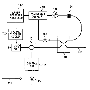
Fig. 7 illustrates a wavelength conversion module in accordance with a further
2o embodiment of the present invention; and
Fig. 8 illustrates a reflectivity characteristic of in-fiber Bragg grating
124.

CA 02309436 2000-OS-02
WO 98/50988 PCT/US98/09283
-5
DETAILED DESCRIPTION
In accordance with the present invention, a microprocessor precisely controls
the wavelength of light output from a laser by monitoring the transmissivity
of a
selectively reflective element, such as an in-fiber Bragg grating, coupled to
the output
of the laser. The Bragg grating has a minimum transmissivity at the desired
output
wavelength of the laser. The microprocessor continually adjusts the wavelength
of
the laser output to obtain substantially minimal transmissivity through the
grating . At
which point, the laser is locked to the desired wavelength. Alternatively, the
1o microprocessor can monitor light reflected from the grating, and
continually adjust the
wavelength of the laser output to lock the laser at a wavelength providing
substantially maximum reflectance by the grating.
Turning to the drawings in which like reference characters indicate the same
or
similar elements in each of the several views, Fig. 1 illustrates a wavelength
conversion module or remodulator 100 in accordance with the present invention.
Remodulator 100 receives an optical input from fiber 110, which is typically
at a
wavelength within the range of 1300 to 1600nm, and is frequently different
than the
desired transmission wavelength to be amplified by erbium doped fibers. The
optical
input typically includes light pulses corresponding to digital communication
data from
2o a SONET terminal, for example. Detector 112, a photodiode, for example,
senses
these light pulses and generates an electrical signal comprising first
electrical pulses in
response thereto. The electrical signal is supplied to control circuit 114,
which

CA 02309436 2005-O1-26
-6-
generates corresponding second electrical pulses of appropriate duration and
amplitude
for driving external modulator 116.
External modulator 116, a Mach-Zehnder modulator, for ex~unple, typically
employs a waveguiding medium whose refractive index changes according to an
applied electrical field. In the Mach-Zehnder modulator, two optical
interferometer
paths are provided. An incoming optical carrier is split between the two
optical paths,
at least one of which is supplied to the waveguiding medium where it is phase
modulated by the applied electric field. When the signal is recombined at the
output,
the light from the paths either constructively or destructively interferes,
depending upon
1o the electrical field applied to the surrounding electrodes during the
travel time of the
carrier. As a result, an amplitude modulated output optical signal can be
obtained.
Returning to Fig. 1, the amplitude modulated output from modulator 116 is
supplied to a coupler 120, which transmits most of the received light: to
output fiber 122
and to the amplifiers, and a remaining portion to a filtering or partially
reflective
element 124. Partially reflective element 124 typically includes an in-fiber
Bragg
grating, such as one described in Morey et al., Photoinduced Bragg Gratings in
Optical
Fibers, Optics & Photonics News, February 1994. Grating 124 typically has a
minimum transmissivity at a wavelength corresponding to the desired output of
laser
118, which is typically a DFB (distributed feedback) semiconductor diode laser
2o generally comprising one or more III-V semiconductor materials commercially
available from a wide variety of suppliers such as Fujitsu, BT&D, GEC Marconi,
and
Hewlett-Packard. In the embodiment illustrated in Fig. 1, long period gratings
having
periods exceeding 100 pm can also be used. Long period gratings are described
in A.
M. Vengsarkar et al., Long-Period Fiber Gratings As Band-Rejection Filters,
Journal of
Lightwave Technology, vol. 14, no. 1, January 1996, pp. 58-65.

CA 02309436 2005-O1-26
_7_
Photodetector 126 senses light transmitted through grating 124, and generates
electrical signals in response thereto. These electrical signals are supplied
to a control
circuit, which may be a hardwired component or a microprocessor, e.g., laser
feedback
control processor 130 (typically a general purpose microprocessor such as a
68302
microprocessor manufactured by Motorolla), which, in turn, supplies an
appropriate
output control voltage, usually a DC voltage, to a thermoelectric cooler 132.
As is
generally understood in the art, the temperature of thermoelectric cooler 132
is adjusted
in response to a voltage applied thereto. Accordingly, laser 118 is preferably
thermally
coupled to thermoelectric cooler 132 so that its temperature can be accurately
to controlled. Typically, thermoelectric cooler 132 can control the
temperature of laser
118 within a range of 15-45°C. Thus, for example, processor 130 can
generate output
control voltages in at least 1 mV increments, which results in precise
incremental
changes in temperature in the range of 0.01-0.05°C.
Generally, the wavelength of light output from laser 118 is inversely related
to
the temperature of laser 118. Accordingly, by changing the temperature of
thermoelectric cooler 132, processor 130 can alter the wavelength of light
output from
laser 118.

CA 02309436 2000-OS-02
WO 98/50988 PCTNS98/09283
_g_
A detailed description of a method for controlling of laser 118 will be
presented below with reference to Figs. 2 and 3. Generally, the method is
carried out
in accordance with a program stored in a memory associated with processor 130.
As seen in Fig. 2, grating 124 has a transmission characteristic which is high
(greater than 60%, for example) for wavelengths significantly greater or less
than a
predetermined wavelength ~,°. At wavelengths approximating ~,°,
however, much of
the incoming light is reflected by the grating and transmissivity dips below
60%, with
the minimum transmissivity occurring at ~,°. Accordingly, the
transmissivity
to characteristic curve shown in Fig. 2 has a "well" 240 centered about
~,° with sloping
sides 220 and 230.
Generally, after processor 130 sets the output wavelength of laser 118 to an
initial value relatively close to ~.°, the wavelength is either
increased or decreased in
relatively large increments until a first "edge" of well 240 is detected,
i.e., a
i5 wavelength at which the transmissivity increases (step 310, Fig. 3). Thus,
for
example, as shown in Fig. 4, laser 118 may be set to an initial wavelength at
point PO
on the transmittance curve. The wavelength may then be increased in relatively
large
increments through points PI and P2 until the transmittance increases at a
wavelength
at point P3. Point P3 corresponds to a first edge. A second edge is then
identified by
2o decreasing the wavelength output from laser 118 in relatively large
increments until a
second edge is located (step 320, Fig. 3). For example, as seen in Fig. 5, the
wavelength is incrementally decreased through points P4 and PS, until the

CA 02309436 2000-OS-02
WO 98/50988 PCT/US98/09283
-9-
transmittance increases at point P6. Laser 118 is then controlled to output
light at a
wavelength between the wavelengths at points P3 and P6 is then output (step
330, Fig.
3) and the wavelength increment is reduced by some factor, e.g., 1/2 (step
340, Fig.
3). It should be noted, however, that although the step of increasing the
wavelength to
locate the first edge has been described as preceding the step of decreasing
the
wavelength to locate the second edge, it is also contemplated that the
wavelength may
be decreased to locate the first edge prior to increasing the wavelength to
locate the
second edge.
1o Processor 130 continuously cycles through steps 310-340. With each
successive iteration, the wavelength increment is reduced, the first and
second edges
are brought closer together, and a new midpoint wavelength is set. The
wavelength
increment is decreased until it reaches a minimum predetermined value. At
which
point, processor 130 repeats the steps of locating first and second edges and
setting
the midpoint wavelength between the two, but with no further reduction in the
incremental changes in wavelength. As a result, the output wavelength is
confined to
within a narrow range in the "cusp" of well 240 and is substantially equal to
the
desired wavelength.
Fig. 6 illustrates in greater detail the process used to control laser 118. In
2o initial step 610, output control voltage increment ~V is initialized to a
relatively large
value OVmax and assigned a positive polarity, for example. As noted above,
changes
in the control voltage output from processor 130 cause changes in the
temperature of

CA 02309436 2000-OS-02
WO 98/50988 PCT/US98/09283
-10-
laser 118, resulting in corresponding changes in the wavelength of light
output from
laser 118. Thus, OV corresponds to the incremental change in wavelength of
light
output from laser 118, such that a large 0V translates to large changes in
output
, wavelength while a small ~V translates to a small change in wavelength.
In step 615 an initial voltage V 1 is output from processor 130. This initial
voltage can be, for example, a previously stored voltage corresponding to a
temperature of thermoelectric cooler 132 which results in an output wavelength
within
well 240 and preferably close to the desired output wavelength ~,o. In step
620, the
1o transmissivity T1 with output control voltage V 1 is measured by sensing a
voltage
output from detector 126 (Fig. 1 ). The output control voltage is then
increased by OV
in step 630, and the resulting transmittance T2 is measured in step 635.
In step 640, a comparison is made to determine whether T2 (the transmittance
at V 1+OV) is less than T1 (the transmittance at V 1 ). If yes, processor 130
assumes
that an edge has not been reached. Accordingly, V 1 is set equal to V 1+pV
(step 645),
and processor 130 repeats steps 615-640. If T2 is greater than T1, however,
processor
130 assumes that an edge has been detected. In which case, processor 130 will
now
attempt to find the second edge of well 240. Thus, the program branches and,
in step
650, 0V is inverted to negative polarity, indicating that the output control
voltage, at
2o this point, is to be decreased incrementally by amounts ~V. Here, in step
660, a
determination is made as to whether OV is positive. Since it is not at this
stage,
VEDGE1 is set to voltage V 1 (step 685), and the value of the control output
voltage
associated with the first edge is temporarily stored in a scratch memory
associated

CA 02309436 2000-OS-02
WO 98/50988 PCTNS98/09283
-11-
with processor 130. Processor 130 again cycles through steps 615-645, thereby
decrementing the output control voltage until the second edge is determined,
i.e., Q
when T2 is greater than T1. The polarity of ~V is again inverted in step 650,
at this
point from negative to positive polarity. In step 660, since ~V is positive,
the
program branches and sets VEDGE2 equal to V l, i.e., the output control
voltage
generating the wavelength at the second edge is stored in processor 130 (step
665).
V 1 is then set to a voltage midway between VEDGE 1 and VEDGE2 (step 670). If
0V is less than a minimum value OVmin (step 675), no further reduction in OV
is
required. On the other hand, if 0V exceeds ~Vmin, 0V is reduced by some
factor,
e.g., %i, in step 680 so that the output control voltage is adjusted in
smaller
increments.
Processor 130 returns to step 615 to output voltage V l, now equal to a
voltage
between VEDGE1 and VEDGE2, thereby setting the temperature of laser 118 so
that
a wavelength substantially between the wavelengths at the first and second
edges is
output from laser 118. Processor 130 next continuously cycles through the
above
steps to locate edges within well 240, supply new midpoint output control
voltages,
and decrease the incremental control voltage 0V with each iteration until 0V
is equal
to OVmin. Thus, as noted above, the edges are spaced closer, and after several
2o iterations, the output wavelength is adjusted to be within the cusp of well
240. At this
point, the wavelength of light output from laser 118 is typically within
approximately
0.02 nm of ?~o, and the frequency of the output light is within 2GHz of a
frequency
corresponding to ~,o. Laser 118 is thus considered locked at wavelength 7~0.

CA 02309436 2000-OS-02
WO 98/50988 PCT/US98/09283
-12-
Typically, gratings with a narrow spectral width will provide a "tighter" lock
in which the wavelength of light output from laser 118 deviates little from
~,°.
Accordingly, gratings having a spectral width of approximately 1 angstrom are
s generally used, although gratings having broader spectral widths can be
utilized as
well.
Typically, processor 130 monitors the temperature of laser 118 to insure that
it
is substantially constant or has stabilized prior to measuring the
transmittance through
grating 124. Such temperature stabilization usually occurs about 1-S seconds
after a
1o new output control voltage is supplied to thermoelectric cooler 132.
Moreover, the
temperature of grating 124 can be continuously monitored so that if it falls
outside a
predetermined range, an alarm signal can be generated and processor 130 will
cease
monitoring of laser 118 and will cease stepping the voltage supplied to
thermoelectric
cooler 132. In which case, processor 130 can notify the user of a fault with
grating
15 124. Further, if the intensity of light sensed by detector 126 falls
outside a
predetermined range, processor 130 can generate the alarm signal, thereby
indicating a
fault with laser 118 or detector 126.
Fig. 7 illustrates a second embodiment of the present invention. The
second embodiment differs from the first embodiment in that it includes a
second
2o photodetector 720 and comparator circuit 730. In accordance with the second
embodiment, grating 124 is both reflective and transmissive at ~,°. For
example, the
maximum reflectivity of grating 124 at ~,° is 70% of incident optical
power and the
corresponding minimum transmissivity is 30%. As further shown in Fig. 7, light

CA 02309436 2000-OS-02
WO 98/50988 PCT/US98/09283
-13-
reflected by grating 124 through coupler 120 is sensed by photodetector 720,
which
generates a voltage signal Vrefl. Photodetector 126, however, detects the
amount of
light transmitted through grating 124, and outputs a voltage signal Vtrans, in
response
thereto. Typically, comparator circuit 730 is configured to receive signals
Vrefl and
Vtrans and output a potential representative of a deviation of the actual
wavelength
output from laser 118 and the desired wavelength ~,o. For example, the output
of
comparator circuit 730 may be substantially equal to (Vtrans + Vrefl)/Vtrans.
Alternatively, the outputs of photodetectors 126 and 720 may be supplied
directly to
1o processor 130, which is appropriately programmed to obtain the quantity
(Vtrans +
Vrefl)/Vtrans.
The same process described above is preferably followed to adjust the output
of laser 118 to be within the cusp of well 240. The second embodiment,
however, is
advantageous in that variations in the power output of laser 118, which would
otherwise cause the transmission characteristic to shift up or down, are
canceled out.
In accordance with a third embodiment, detector 126 and comparator circuit
730 can be omitted such that laser feedback processor 130 monitors the
reflectivity of
grating 124 by receiving Vrefl only. As shown in Fig. 8, the reflectivity
characteristic
of grating 124 typically has a maximum reflectance or peak at ~,o. In order to
lock
laser 118 within a narrow range about 7~0, processor 130, in this instance
follows
substantially the same process described above with reference to Fig. 6 with
the
exception that reflectivity of grating 124 is monitored instead of
transmissivity.
Moreover, edges are identified at wavelengths where the reflected light
decreases, not

CA 02309436 2000-OS-02
WO 98/50988 PCT/US98/09283
->< a-
where transmissivity increases. Thus, at step 640, for example, the program
will
branch to invert the polarity of OV if the reflectivity at V 1 is less than
the reflectivity
at V 1+OV. Otherwise, the program is substantially the same, and the
wavelength will
be adjusted to within a narrow range substantially centered about the peak of
the
reflectivity characteristic.
Further, in accordance with a fourth embodiment the circuit shown in Fig. 7
may be used to cancel out optical power variations, while restricting the
wavelength
of light output from laser 118 to be substantially centered at the
reflectivity peak. In
to which case, however, comparator circuit 730 can be appropriately
configured, for
example, to supply the quantity (Vtrans + Vrefl)/Vrefl to processor 130.
Alternatively, comparator circuit 730 may be omitted, and processor 130 may be
appropriately programmed to generate this parameter in response to direct
application
of Vrefl and Vtrans.
While the foregoing invention has been described in terms of the embodiments
discussed above, numerous variations are possible. Accordingly, modifications
and
changes such as those suggested above, but not limited thereto, are considered
to be
within the scope of the following claims.

Dessin représentatif
Une figure unique qui représente un dessin illustrant l'invention.
États administratifs

2024-08-01 : Dans le cadre de la transition vers les Brevets de nouvelle génération (BNG), la base de données sur les brevets canadiens (BDBC) contient désormais un Historique d'événement plus détaillé, qui reproduit le Journal des événements de notre nouvelle solution interne.

Veuillez noter que les événements débutant par « Inactive : » se réfèrent à des événements qui ne sont plus utilisés dans notre nouvelle solution interne.

Pour une meilleure compréhension de l'état de la demande ou brevet qui figure sur cette page, la rubrique Mise en garde , et les descriptions de Brevet , Historique d'événement , Taxes périodiques et Historique des paiements devraient être consultées.

Historique d'événement

Description Date
Inactive : Périmé (brevet - nouvelle loi) 2018-05-08
Requête pour le changement d'adresse ou de mode de correspondance reçue 2018-01-09
Inactive : CIB expirée 2013-01-01
Inactive : CIB désactivée 2011-07-29
Inactive : CIB de MCD 2006-03-12
Accordé par délivrance 2005-11-15
Inactive : Page couverture publiée 2005-11-14
Préoctroi 2005-08-26
Inactive : Taxe finale reçue 2005-08-26
Un avis d'acceptation est envoyé 2005-03-09
Lettre envoyée 2005-03-09
Un avis d'acceptation est envoyé 2005-03-09
Inactive : Approuvée aux fins d'acceptation (AFA) 2005-02-14
Modification reçue - modification volontaire 2005-01-26
Inactive : Dem. de l'examinateur par.30(2) Règles 2004-07-26
Lettre envoyée 2003-03-03
Requête d'examen reçue 2003-02-05
Exigences pour une requête d'examen - jugée conforme 2003-02-05
Toutes les exigences pour l'examen - jugée conforme 2003-02-05
Lettre envoyée 2000-07-27
Inactive : Page couverture publiée 2000-07-21
Inactive : CIB en 1re position 2000-07-12
Inactive : Lettre de courtoisie - Preuve 2000-07-11
Inactive : Notice - Entrée phase nat. - Pas de RE 2000-07-05
Demande reçue - PCT 2000-06-29
Inactive : Transfert individuel 2000-06-12
Demande publiée (accessible au public) 1998-11-12

Historique d'abandonnement

Il n'y a pas d'historique d'abandonnement

Taxes périodiques

Le dernier paiement a été reçu le 2005-04-25

Avis : Si le paiement en totalité n'a pas été reçu au plus tard à la date indiquée, une taxe supplémentaire peut être imposée, soit une des taxes suivantes :

  • taxe de rétablissement ;
  • taxe pour paiement en souffrance ; ou
  • taxe additionnelle pour le renversement d'une péremption réputée.

Les taxes sur les brevets sont ajustées au 1er janvier de chaque année. Les montants ci-dessus sont les montants actuels s'ils sont reçus au plus tard le 31 décembre de l'année en cours.
Veuillez vous référer à la page web des taxes sur les brevets de l'OPIC pour voir tous les montants actuels des taxes.

Titulaires au dossier

Les titulaires actuels et antérieures au dossier sont affichés en ordre alphabétique.

Titulaires actuels au dossier
CIENA CORPORATION
Titulaires antérieures au dossier
STEPHEN R. HARMON
VICTOR MIZRAHI
Les propriétaires antérieurs qui ne figurent pas dans la liste des « Propriétaires au dossier » apparaîtront dans d'autres documents au dossier.
Documents

Pour visionner les fichiers sélectionnés, entrer le code reCAPTCHA :


Pour visualiser une image, cliquer sur un lien dans la colonne description du document. Pour télécharger l'image (les images), cliquer l'une ou plusieurs cases à cocher dans la première colonne et ensuite cliquer sur le bouton "Télécharger sélection en format PDF (archive Zip)" ou le bouton "Télécharger sélection (en un fichier PDF fusionné)".

Liste des documents de brevet publiés et non publiés sur la BDBC .

Si vous avez des difficultés à accéder au contenu, veuillez communiquer avec le Centre de services à la clientèle au 1-866-997-1936, ou envoyer un courriel au Centre de service à la clientèle de l'OPIC.


Description du
Document 
Date
(aaaa-mm-jj) 
Nombre de pages   Taille de l'image (Ko) 
Dessin représentatif 2000-07-20 1 5
Abrégé 2000-05-01 1 52
Description 2000-05-01 14 571
Revendications 2000-05-01 14 450
Dessins 2000-05-01 6 82
Description 2005-01-25 14 557
Revendications 2005-01-25 12 402
Dessin représentatif 2005-02-28 1 6
Avis d'entree dans la phase nationale 2000-07-04 1 192
Courtoisie - Certificat d'enregistrement (document(s) connexe(s)) 2000-07-26 1 115
Rappel - requête d'examen 2003-01-08 1 113
Accusé de réception de la requête d'examen 2003-03-02 1 185
Avis du commissaire - Demande jugée acceptable 2005-03-08 1 162
Correspondance 2000-07-04 1 14
PCT 2000-05-01 9 318
Correspondance 2005-08-25 1 29