Note : Les descriptions sont présentées dans la langue officielle dans laquelle elles ont été soumises.
r CA 02310345 2000-OS-31
Arnett 40-12-13 1
ENHANCED COMMUNICATION CONNECTOR ASSEMBLY WITH CROSSTALK
COMPENSATION
Field Of The Invention
This invention relates generally to communication
connectors, and particularly to a connector assembly that
compensates for crosstalk among different signal paths
conducted through the assembly.
Discussion Of The Known Art
There is a need for a durable, high frequency
communication connector assembly that compensates for
(i.e., cancels or reduces) crosstalk among and between
different signal paths within the assembly. As broadly
defined herein, crosstalk occurs when signals conducted
over a first signal path, e.g., a pair of terminal contact
wires associated with a communication connector, are partly
transferred by inductive or capacitive coupling into a
second signal path, e.g., another pair of terminal contact
wires in the same connector. The transferred signals
define "crosstalk" in the second signal path, and such
crosstalk degrades any signals that are routed over the
second path.
For example, an industry type RJ-45 communication
connector has four pairs of terminal wires defining four
different signal paths. In typical RJ-45 plug and jack
connectors, all four pairs of terminal wires extend closely
parallel to one another over the lengths of the connector
bodies. Thus, signal crosstalk may be induced between and
among different pairs of terminal wires within the typical
RJ-45 plug and jack connectors, particularly when the
connectors are in a mated configuration. The amplitude of
r
CA 02310345 2004-02-10
2
the crosstalk becomes stronger as the coupled signal
frequencies or data rates increase.
Applicable industry standards for rating the degree to
which communication connectors exhibit crosstalk, do so in
terms of so-called near end crosstalk or "NEXT". Moreover,
NEXT ratings are typically specified for mated connector
configurations, e.g., a type RJ-45 plug and jack
combination, wherein the input terminals of the plug
connector are used as a reference plane. Communication
links using unshielded twisted pairs (UTP) of copper wire
are now expected to support data rates up to not only 100
MHz, or industry standard "Category 5" performance; but to
meet "Category 6" performance levels which call for at least
46 dB crosstalk isolation at 250 MHz.
U.S. Patent 5,186,647, issued February 16, 1993,
(Denkmann et al.) which is assigned to the assignee of the
present invention and application, discloses an electrical
connector for conducting high frequency signals. The
connector has a pair of metallic lead frames mounted flush
with a dielectric spring block, with connector terminals
formed at opposite ends of the lead frames. The lead frames
themselves include flat elongated conductors each of which
includes a spring terminal contact wire at one end for
contacting a corresponding terminal wire of a mating
connector, and an insulation displacing connector terminal
at the other end for connection with an outside insulated
wire lead. The lead frames are placed over one another on
the spring block, and three conductors of one lead frame
have cross-over sections configured to overlap corresponding
cross-over sections formed in three conductors of the other
CA 02310345 2004-02-10
3
lead frame. U.S. Patent 5,580,270 (Dec. 3, 1996) also
discloses an electrical plug connector having crossed pairs
of contact strips.
Crosstalk compensation circuitry may also be provided
on or within layers of a printed wire board, to which spring
terminal contact wires of a communication jack are connected
within the jack housing. See U.S. Patent 5,997,358, issued
December 7, 1999. See also U.S. Patent 5,299,956
(Apr. 5, 1994).
U.S. Patent 6,116,964, issued September 12, 2000,
discloses a communications connector assembly having
co-planar terminal contact wires, wherein certain pairs of
the contact wires have opposed cross-over sections to
provide inductive crosstalk compensation.
Further, U.S. Patent 5,547,405 (Aug. 20, 1996)
discloses an electrical connector having signal carrying
contacts that are stamped as lead frames from a metal sheet.
Certain contacts have integral lateral extensions that
overlie enlarged adjacent portions of other contacts to
provide capacitive coupling crosstalk compensation. A
dielectric spacer is disposed between an extension of one
contact and an enlarged adjacent portion of the other
contact. Thus, the stamped lead frames for the connector of
the '405 patent are complex, and are relatively difficult to
manufacture and assemble precisely.
CA 02310345 2004-02-10
4
There remains a need for a communication jack connector
assembly which, when mated with a typical RJ-45 plug,
provides both inductive and capacitive crosstalk
compensation such that the mated connectors will meet or
surpass Category 6 performance.
Summary Of The Invention
According to the invention, a communications connector
assembly includes a wire board, and a number of elongated
terminal contact wires each having a base portion supported
on the wire board, and a free end portion opposite the base
portion to make electrical contact with a mating connector.
A crosstalk compensating device on the wire board cooperates
with sections of selected terminal contact wires to produce
a determined amount of capacitive compensation coupling
between the selected terminal contact wires, when the
contact wires are engaged by the mating connector.
In one embodiment, the wire board of the communication
connector assembly is inserted within a jack housing, and an
opening in a front surface of the jack housing is
dimensioned for receiving the mating plug connector.
In accordance with one aspect of the present invention
there is provided an enhanced communication connector
assembly, comprising: a wire board; a number of elongated
terminal contact wires each having a base portion supported
on the wire board, a free end portion opposite said base
portion for making electrical contact with a mating
connector, and a section connecting the free end portion and
the base portion with one another; the free end portion is
arranged so that the section of the terminal contact wire
CA 02310345 2004-02-10
4a
deflects by the action of the mating connector; and a first
crosstalk compensating device fixed on the wire board,
wherein the device is constructed and arranged to engage
with the sections of selected terminal contact wires to
provide capacitive compensation coupling between the
selected terminal contact wires when the sections of the
contact wires are deflected by said mating connector.
In accordance with another aspect of the present
invention there is provided an enhanced communications jack
connector comprising: a jack housing having a front
surface and a plug opening in said front surface, wherein
the plug opening has an axis and is formed to receive a
mating plug connector; and a communication connector
assembly inserted in said jack housing for making electrical
contact with said mating plug connector when the plug
connector is inserted along the axis of the plug opening in
the jack housing, said connector assembly comprising; a wire
board supported in the jack housing; a number of elongated
terminal contact wires each having a base portion supported
on the wire board, a free end portion opposite said base
portion for electrically contacting a corresponding terminal
of the mating plug connector, and a section connecting the
free end portion and the base portion with one another; the
free end portion is configured so that the section of the
terminal contact wire deflects by the action of the mating
plug connector; and a first crosstalk compensating device
fixed on the wire board, wherein the device is constructed
and arranged to engage with the sections of selected
terminal contact wires to provide capacitive compensation
coupling between the selected terminal contact wires when
CA 02310345 2004-02-10
4b
the sections of the contact wires are deflected by said
mating plug connector.
For a better understanding of the invention, reference
is made to the following description taken in conjunction
with the accompanying drawings and the appended claims.
Brief Description Of The Drawings
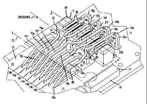
FIG. 1 is a perspective view of a communication
connector assembly, and a jack housing into which the
assembly can be inserted and mounted;
CA 02310345 2000-OS-31
Arnett 40-12-13 5
. FIG. 2 is an enlarged, perspective view of a front
portion of the connector assembly in FIG. l;
FIG. 3 is a side view, partly in section, of the front
portion of the connector assembly in FIG. 2;
FIG. 4 is a sectional view of the connector assembly,
as taken along line 4-4 in FIG. 3;
FIG. 5 is a plan view, of a plate capacitor circuit;
FIG. 6 is a perspective view showing the capacitor
circuit of FIG. 5 mounted on the connector assembly; and
FIG. 7 is an electrical schematic representation of
the connector assembly with capacitive crosstalk
compensation coupling between sections of terminal contact
wires.
Detailed D~scription Of The Invention
FIG. 1 is a perspective view of an enhanced
communication connector assembly 10, and a communication
jack frame or housing 12 into which the assembly 10 can be
inserted and mounted. The jack housing 12 has a front face
in which a plug opening 13 is formed. The plug opening 13
has an axis P, along the direction of which axis a mating
plug connector may be inserted into the housing opening 13
to connect electrically with the assembly 10. FIG. 2 is an
enlarged, perspective view of a front portion of the
connector assembly 10 in FIG. 1.
In the illustrated embodiment, the communication
connector assembly 10 has an associated, generally
rectangular printed wire board 14. The board 14 may
comprise, for example, a single or a multi-layer dielectric
substrate. A number, e.g., eight elongated terminal
CA 02310345 2000-OS-31
Arnett 40-12-13
contact wires 18a-18h emerge from a central portion of the
printed wire board 14, as seen in FIG. 1. The contact
wires 18a-18h extend substantially parallel to one another,
and are generally uniformly spaced from a top surface 15 of
a two-part contact wire guide structure 16. A first
support part 17 of the guide structure 16 is fixed on a
front portion of the wire board 14.
A second support part 19 is fixed to a front end of
the first support part 17, and projects in a forward
direction from the wire board 14, as shown in FIGS. 1 and
3. The second support part 19 of the guide structure has a
number of parallel channels opening in the top surface 15,
for pre-loading and for guiding the free end portions of
corresponding contact wires, as shown in FIGS. 1-3.
The contact wires are formed and arranged to deflect
resiliently toward the top surface 15 of the guide
structure 16, when free end portions 70a to 70h of the
wires are engaged by a mating connector along a direction
parallel to the top surface. The material forming the
terminal contact wires 18a-18h may be a copper alloy, e.g.,
spring-tempered phosphor bronze, beryllium copper, or the
like. A typical cross-section of the terminal contact
wires 18a-18h is 0.015 inches square.
The wire board 14 may incorporate conductive traces,
electrical circuit components or other devices arranged to
compensate for connector-induced crosstalk. Such devices
can include wire traces printed within layers of the board,
such as are disclosed in the mentioned '741 application.
Any crosstalk compensation provided by the board 14 may be
in addition to, and cooperate with, an initial stage of
crosstalk compensation provided by the terminal contact
r
~
CA 02310345 2000-OS-31
Arnett 40-12-13 7
wires 18a-18h and the contact wire guide structure 16 on
the board 14, as explained below.
The terminal contact wires 18a-18h have upstanding
base portions 20a-20h that are electrically connected at
one end to conductors associated with the wire board 14.
For example, contact leg or ~tail" ends of the base
portions 20a-20h may be soldered or press-fit into
corresponding plated terminal openings in the board 14, to
connect with conductive traces or other electrical
components on or within one or more layers of the board 14.
The base portions 20a-20h connect with the board 14
with an alternating offset in the long direction of the
contact wires 18a-18h. This offset configuration is
necessary to allow a relatively close center-to-center
spacing of, e.g., 0.040 inches between adjacent free end
portions of the contact wires, without requiring the same
close spacing between adjacent plated terminal openings in
the board 14. Otherwise, adjacent terminals on the board
may ~short" with one another. While the offset
configuration of the contact wire base portions 20a-20h
shown in FIGS. 1 and 2 provides satisfactory results, other
configurations may also be acceptable. For example, an
alternating ~saw-tooth" pattern where three or more
consecutive terminal openings in the board 14 are aligned
to define an edge of each tooth, may also offer acceptable
performance in certain applications. Accordingly, the
illustrated offset pattern is not to be construed as a
limitation in the manufacture of the connector assembly 10,
as long as adjacent plated terminal openings in board 14
are spaced far enough apart to prevent electrical shorting.
The wire board 14 has a wire connection terminal
region 52 (FIG. 1) at which outside, insulated wire leads
t
CA 02310345 2004-02-10
8
are connected to an array of contact terminals (not shown)
located in the region 52. Such terminals may be so-called
insulation displacing connector (IDC) terminals each of
which has a leg part connected to a conductive trace on the
board 14, which trace is associated with one of the terminal
contact wires 18a-18h. The wire connection terminal region
52 may be enclosed by a terminal housing on the top side of
the board 14, and a cover on the bottom side of the board.
See U.S. Patent 5,924,896, issued July 20, 1999.
As seen in FIGS. 2 & 3, the free end portions 70a-70h
of the terminal contact wires have a downwardly arching
configuration, and project beyond a front edge 71 of the
wire board 14. The free end portions 70a-70h are supported
in cantilever fashion by the base portions 20a-20h of the
contact wires, wherein the base portions are supported by
the board 14. The free end portions of the contact wires
define a line of contact 72 (FIG. 2) transversely of the
contact wires, and the wires make electrical contact with a
mating connector at points along the line of contact 72.
When the contact wires 18a-18h engage corresponding
terminals of a mating connector, the free end portions
70a-70h cantilever in the direction of the top surface 15 of
the contact wire guide structure 16, i.e., toward the wire
board 14.
In the following disclosure, pairs of the eight terminal
contact wires 18a-18h are sometimes referred to by pair
numbers, from wire pair no. 1 to pair no. 4, as follows.
CA 02310345 2000-OS-31
Arnett 40-12-13 9
Pair No. Terminal Contact Wires
1 18d, 18e
2 18a, 18b
3 18c, 18f
4 18g, 18h
As seen in FIGS. 1-3, pair nos. 1, 2 and 4 of the
terminal contact wires have cross-over sections 74, at
which each contact wire of a given pair steps toward and
crosses above or below the other contact wire of the pair,
with a generally ~S"-shaped side-wise step 76. The
terminal contact wires are also curved arcuately above and
below their common plane at each cross-over section 74, as
shown in FIG. 3. Opposing faces of the steps 76 in the
contact wires are spaced apart typically by about .035
inches (i.e., enough to prevent shorting when the terminal
wires are engaged by a mating connector). A typical length
of each cross-over section in the long direction of the
terminal contact wires, is approximately 0.144 inches.
The cross-over sections 74 in the terminal contact
wires 18a-18h serve to initiate inductive crosstalk
compensation coupling among the contact wires, in a region
where the wires are co-planar. See the earlier-mentioned
'506 application. This region extends from a center line
of the cross-over sections 74 to another line 77 where
alternate ones of the terminal contact wires bend toward
the wire board 14. The remaining terminal contact wires
continue to extend above the board 14 from the line 77,
until they too bend toward the board 14. The length of the
co-planar region of inductive crosstalk compensation is,
e.g., approximately 0.180 inches.
r
. CA 02310345 2000-OS-31
Arnett 40-12-13 10
In the illustrated embodiment, the cross-over sections
74 are provided on pair nos. 1, 2 and 4 of the eight
terminal contact wires 18a-18h. The ~pair 3" contact
wires, i.e., wires 18c, 18f, straddle contact wire pair 1
(contact wires 18d, 18e) and no cross-over section is
formed in the contact wires 18c, 18f. That is, each of the
contact wires 18c, 18f, extends above the wire board 14
without a side-wise step. Pairs of terminal contact wires
having the cross-over sections 74 are disposed at either
side of each of the "straight" contact wires 18c, 18f.
The cross-over sections 74 are relatively close to the
line of contact 72. A typical distance between the line of
contact 72 and a center line of the cross-over sections 74,
is approximately 0.149 inches. Accordingly, inductive
crosstalk compensation by the connector assembly 10 starts
near the line of contact 72, beginning with the cross-over
sections 74.
Further details of the contact wire guide structure 16
in FIGS. 1-3, now follow. The first support part 17 of the
structure 16 has a generally ~L"-shaped profile, and is
mounted on a front portion of the wire board 14 next to the
terminal region 52. The support part 17 is secured on the
top surface of the board by one or more ribbed mounting
posts 80 that are press fit into corresponding openings 82
formed in the board 14. See FIG. 3.
An elongated, generally rectangular block 84 projects
upward from a rear end portion of the support part 17. The
block 84 forms, e.g., eight substantially evenly spaced-
apart openings or slots 86 that open in a top surface of
the block. Each slot 86 is located in the block 84 to
receive a section of a corresponding one of the terminal
contact wires 18a-18h. Components associated with the block
y
CA 02310345 2000-OS-31
Arnett 40-12-13 11
84 function to produce or inject an initial stage of
capacitive crosstalk compensation coupling between sections
of selected ones of the terminal contact wires, as
explained further below.
The second support part 19 acts to apply a certain
pre-load bias force F on the free end portions of the
terminal contact wires, in the direction of the arrow in
FIG. 3. The part 19 also has associated ribbed mounting
posts 85 that are press.fit into corresponding holes 87
formed in the board 14, near the board front edge 71 as
shown in FIG. 3.
Eight parallel channels 89 are cut in the top surface
of the second support part 19. The channels 89 are located
to align with and receive corresponding free end portions
70a-70h of the terminal contact wires, and to guide the
free end portions when they are deflected by the action of
a mating plug connector. A front end portion 90 of the
second support part 19 is configured to apply the pre-load
bias force F to the free end portions of the contact wires
in each of the channels 89, as shown in FIG. 3.
As mentioned, the block 84 of the first support part
17 has associated components that produce capacitive
coupling between sections of certain terminal contact
wires, for the purpose of capacitive crosstalk
compensation. A cross-section view through one of the
contact wire slots 86 in the block 84, is shown in FIG. 3.
To suppress crosstalk between terminal contact wire pair
nos. 1 and 3, larger values of capacitive coupling are
needed between adjacent sections of the terminal contact
wires 18c & 18e, and between sections of the wires 18d &
18f; with respect to any capacitance coupling introduced
between sections of the remaining wires in the slots 86.
r
~
CA 02310345 2000-OS-31
Arnett 40-12-13 12
An additional stage or stages of crosstalk compensation on
the wire board 14 may then be provided in a manner
disclosed, for example, in the mentioned U.S. Patent
Application No. 08/923,741. Such additional stage or
stages may then effectively cancel or substantially reduce
crosstalk that would otherwise be present at output
terminals of the assembly 10 corresponding to the terminal
contact wire pair nos. 1 and 3.
Increased capacitive coupling between adjacent
sections of contact wire pair nos. 1 and 3 in the slots 86,
is produced by a pair of compensation plate capacitors 100
that are supported by the block 84. Dielectric portions of
the capacitors 100 form walls between those slots 86 in
which adjacent sections of wires 18c & 18e, and 18d & 18f,
are contained. The plate capacitors 100 are aligned with
and connect electrically to the mentioned contact wire
sections when the connector assembly 10 is engaged by a
mating connector, as explained below. Thus, capacitive
crosstalk compensation coupling is injected relatively
close to the line of contact 72, and to the crossover
section 74 of contact wire pair no. 1.
Each of the plate capacitors 100 comprises a generally
rectangular base dielectric 102 of, for example, a
polyamide film material having a dielectric constant (E) of
about 3.5. An upper portion of the dielectric 102 also
forms a partition wall between adjacent slots 86 in the
block 84, as seen in FIG. 4. A pair of electrically
conductive capacitor plates 104, 106, are deposited or
otherwise adhered on opposite sides of the base dielectric
102. In the illustrated embodiment, capacitor plate 104
has less area then capacitor plate 106. Thus, precise
alignment between the plates 104, 106, is not necessary to
obtain a desired value of capacitance. That is, the
CA 02310345 2004-02-10
13
capacitive coupling produced by each capacitor 100 is a
function of the area of the smaller plate 104, and a slight
misalignment of the plates 104, 106, relative to one
another will not vary the capacitance value which is
expressed by the following equation:
EA
C=
4~~t,~x9x10~ (Eq. 1)
wherein: E = dielectric constant of base dielectric 102
A = area of conductive plate 104 in square
centimeters
tl = thickness of base dielectric 102 in
centimeters
Each of the capacitor plates 104, 106, has one or more
points of contact or "bumps" 108 along a top edge of the
plate. See FIG. 3. The thicknesses (tz) of the plates
104, 106, are such that the corresponding contact wire
sections will make satisfactory electrical contact with the
bumps 108 on the plates when a mating connector causes the
wire sections to be urged downward within the slots 86, as
viewed in FIGS. 3 and 4. The bumps 108 assure a good
contact between the plates 104, 106, and the cooperating
sections of terminal contact wires. The bumps 108 may, for
example, be curved sharply at the top so as to cause any
foreign material to be dislodged when a contact wire
section is urged against a point of contact on the bump.
Capacitive coupling between adjacent sections of
contact wires 18c & 18e, and between adjacent sections of
wires 18d & 18f, by an amount more than 14 times that
produced between adjacent section of contact wires 18d &
18e was obtained under the following conditions, wherein t
is the distance between plates 106, 104 of the two plate
~
CA 02310345 2000-OS-31
Arnett 40-12-13 14
capacitors 100, which plates directly oppose one another in
the dielectric block 84 (see FIG. 4):
Ratio of spacing ~1 - 12.3
Dielectric constant of
base dielectric 102 - 3.5
Dielectric constant of
block 84 - 3.0
FIGS. 5 and 6 show an alternative arrangement to
inject capacitive coupling for crosstalk compensation
between sections of certain terminal contact wires, at the
block 84 on the board 14. A double-sided, flexible plate
capacitor circuit 120 in FIG. 5 is formed from a generally
rectangular, elongated flexible film base dielectric 122
such as, e.g., polyamide. A pair of electrically
conductive capacitor plates 124 are formed on a front side
of the base dielectric 122, at areas near opposite ends of
the base dielectric. A pair of flexible connection strips
126 are formed with conductive material also on the front
side of the dielectric 122, and the strips 126 connect
electrically with the capacitor plates 124. The connection
strips 126 extend substantially perpendicular to the long
axis of the base dielectric 122.
Another pair of conductive capacitor plates 128 are
formed on the rear side of the base dielectric 122, behind
the plates 124 on the front side. The area of a rear plate
128 may be less than that of the opposed front. plate 124,
as long as a known area of the rear plate is fully opposed
by the front plate. Thus, the plates of each set need not
. CA 02310345 2000-OS-31
Arnett 40-12-13 15
be precisely aligned with one another to produce a desired
value of capacitance. That is, the known area of each
smaller plate 128 may be used to define the capacitance
value in accordance with Eq. (1), above.
A second pair of connection strips 130 are formed with
conductive material on the front side of the base
dielectric 122. The strips 130 extend substantially
perpendicular to the axis of the base dielectric 122, and
between the two connection strips 126 associated with the
larger capacitor plates 124. A pair of terminal posts or
vias 132 extend through the base dielectric 122 and
electrically connect the ends of the strips 130 at the
front side of the dielectric, to the smaller conductive
plates 128 on the rear side.
FIG. 6 shows the flexible plate capacitor circuit 120
secured along a front wall of the dielectric block 84 on
the first support part 17 of the terminal support structure
16. The connection strips 126, 130, are folded to extend
horizontally along bottom surfaces of corresponding slots
86 in the block 84, beneath the sections of selected
terminal contact wires. The contact wire sections thus
make electrical contact with the connection strips 126,
130, when the contact wires are urged against the strips in
the slots 86 by the action of a mating connector. Free
ends of the strips 126, 130, may be held in place by a
dielectric ledge at a back wall of the block 84.
Alternatively, the strip ends may be secured against the
bottom surfaces of the slots 86 with an acrylic pressure
sensitive adhesive.
FIG. 7 is a schematic representation of the connector
assembly 10. Free end portions of the terminal contact
wires 18a-18h appear beneath the line of contact 72 in FIG.
CA 02310345 2000-OS-31
Arnett 40-12-13 16
7, and cross-over sections 74 in terminal pair nos. 1, 2
and 4 appear above the line of contact 72. Plate
capacitors 100 within the contact wire guide structure 16,
are connected between contact wires 18c & 18e, and between
contact wires 18d & 18f, just above the cross-over section
74 formed by terminal wire pair no. 1 (18d & 18e).
It is believed that Category 6 crosstalk isolation may
be achieved when the connector assembly 10 is mated with an
existing plug connector, if the value of each compensation
plate capacitor 100 is about 2.0 picofarads (pf) and two
additional stages of crosstalk compensation are provided
within the wire board 14. Enhanced performance may also be
obtained with the connector assembly 10 if the value of the
plate capacitors 100 is about 1.2 pf and one additional
stage of crosstalk compensation is provided on the board
14. If no additional crosstalk compensation is provided by
the board 14, the capacitors 100 may have a value of about
0.72 pf and satisfactory performance may still be obtained.
In summary, the connector assembly 10 described and
illustrated herein, provides:
(1) Enhanced capacitive crosstalk compensation
coupling among selected terminal contact wires.
(2) A relatively short distance between the line of
contact 72 with a mating connector, and the position of the
cross-over sections 74 where co-planar inductive crosstalk
compensation begins, thus minimizing signal transmission
delays and improving crosstalk cancellation performance;
(3) A relatively short distance between the position
of the cross-over sections 74 where co-planar, inductive
crosstalk compensation begins, and the position at which
capacitive compensation is injected. This also minimizes
. CA 02310345 2000-OS-31
Arnett 40-12-13 17
signal transmission delays and improves cross-talk
cancellations and
(4) A substantial reduction in the size and
complexity of additional crosstalk compensation stages that
may be needed within the limited space of the printed wire
board 14.
While the foregoing description represents preferred
embodiments of the invention, it will be obvious to those
skilled in the art that various changes and modifications
may be made, without departing from the spirit and scope of
the invention pointed out by the following claims.