Note : Les descriptions sont présentées dans la langue officielle dans laquelle elles ont été soumises.
CA 02310853 2000-06-06
A Modular, Expandable and Reconfigurable Optical Switch
Abstract
A method and apparatus is disclosed for a modular and expanda lcal switch that
transfers optical signals arriving at a multiplicity of inpu its to distinct
output ports. A
basic switching unit is disclosed that transfers n i optical signals to n
distinct output
signals under the control of digital electrons 'gnats. Apparatus and methods
are
disclosed for building said n by n bas' itching units using electrooptic wafer
beam
deflectors. Methods are disclo or building larger N input by N output optical
switches by interconne g and controlling arrays of basic switching units.
Finally,
methods are disc d for building even larger optical switches by using
wavelength-
division plexing and demultiplexing at the input and output ports of an N x N
opt' switch.
Field of invention
The present invention in general relates to optical switches used in
telecommunications
and computer networks to switch and route optical signals arnving in one or a
plurality of
input ports to one or a plurality of output ports.
Optical transmission technologies have increased the information-carrying
capacity of a
single optical fiber to more than 1 Terabit per second. Future switches must
therefore be
able to transfer aggregate information rates in the many Terabits per second.
Electronic
switches that can handle these information rates are extremely difficult to
build because
of the relatively-limited information-carrying capacity of electronic systems.
Optical
switches that transfer information in optical form can avoid the bottleneck
inherent in
electronic switches.
Optical switches differ in terms of the type of optical signals they can
transfer and in
terms of the rate at which the switch interconnection pattern can be
reconfigured. Some
optical switches can transfer optical signals spanning a broad range of
wavelengths, while
other optical switches are limited to transferring individual wavelengths.
Most optical
switches are reconfigured infrequently and require relatively long time
periods to
reconfigure.
More specifically, the present invention relates to optical switches that are:
1. modular in
design and can be built from small to large number of port counts; 2. flexible
in the type
of optical signals that can be carried, from single wavelengths, to bands of
wavelengths,
to broad regions of optical spectrum; 3. rapidly reconfigurable. The present
invention
can be used in optical switches and routers in telecommunications and computer
networks.
CA 02310853 2000-06-06
Discussion of Previous Art
The transmission of information over optical fiber systems provides the
advantages of
extremely high transmission rates (measured in bits per second) and extremely
low bit
error rates. The design of electronic switches to transfer information among
optical fiber
systems is very challenging because of the extremely large volumes of
information that
must be handled electronically. All-optical switches transfer information
among optical
fiber systems without converting the information streams into electronic form,
and hence
avoid the electronic bottleneck inherent in electronic switches. In this
patent we disclose
a novel optical switch that is constructed from multiple basic switching units
and that
possesses the desireable properties of low loss, high switching speed, and
modular
expandibility.
The design of an optical switch involves the routing of an incoming optical
signal along a
desired path. This routing can be accomplished in a number of ways. Mechanical
force
can be used to move the incoming optical fiber so that it is aligned with the
desired
outgoing optical fiber [Personick 1987, pg. 6]. Mechanical force can also be
used to
control the incidence angle between an incoming light beam and a mirror in
order to
reflect the beam to a desired output optical fiber. This approach is used in
micro-
electromechanical systems [Stern 1999, pg. 228].
Electro-optic effects are also used to control the routing of an optical
signal. The index
of refraction of a substrate such as lithium niobate can be controlled through
the
application of an electric field created by a voltage applied to across a slab
of material.
Regions of higher index of refraction in a substrate can be created by an ion
exchange
process. A 2x2 optical crosspoint can be produced by creating regions of
higher
refractive index in the shape of two channels or optical waveguides. Voltage
control
signals can then be used to direct two incident optical signals to the desired
output ports
[Personick 1987, pg. 6]. Larger n input by n output optical switching fabrics
can be
constructed from elementary 2x2 crosspoints using a crossbar arrangement
[Nakajima
1999]. Even larger NxN optical switching fabrics can be constructed from nxn
basic
switching fabrics using Clos and Benes multistage switch constructions [Hui
1990, pp.
70-77].
The feasibility of constructing large switches from elementary components such
as 2x2
waveguide-based crosspoints is determined by several factors. The loss in
signal power
incurred in traversing each component determines the maximum number of stages
that
can be traversed without amplification. The crosstalk that results when the
power in one
optical signal leaks into another signal affects the integrity of the
information that
traverses the fabric. The time required to reconfigure each component
determines the
rate at which the overall switch fabric can be reconfigured.
Typically, electromechanical switching systems control crosstalk by
controlling the
distance between different optical signals so very low crosstalk levels can be
achieved.
However the reconfiguration rate of electromechanical systems is typically in
the order of
1 kHz. Electro-optic effect systems can be reconfigured at much faster rates,
1 MHz or
2
CA 02310853 2000-06-06
higher. Unfortunately electro-optic waveguide-based systems can suffer from
significant
crosstalk impairment and/or significant loss levels.
A recent approach to routing optical signals using an electro-optic effect
involves the
forming of a series of prisms in a segment of a substrate [Chiu 1995], [Li
1996], [Stancil,
199x]. Reversing the ferroelectric polarization in triangular-shaped regions
in a substrate
forms prisms. The value of an applied voltage across the substrate controls
the deflection
angle of a light beam as it propagates through the substrate, and hence
determines the
point at which the beam exits the substrate. We refer to this novel switching
component
as an "electrooptic wafer beam deflector." The speed at which the exit point
of a light
beam in this component can be reconfigured is limited essentially by the speed
of the
control voltage signal. The optical signal undergoes very low loss in
traversing the
component [Li 1996]. The electrooptic wafer beam deflector component provides
a
preferred embodiment for the optical switch designs disclosed in this
document.
Several methods have been developed for the construction of optical switch
fabrics from
splitter and combiner components. [Spanke, 1987] proposed a multiple-substrate
n x n
optical switch architecture based on 1 x n splitters and n x 1 combiners which
has good
properties in terms of signal-to-noise ratio across a fabric constructed from
waveguide-
based switch components. [Dial 1988] proposed an n x n optical switch
involving
passive splitters, passive combiners, and spatial light modulators that
control the transfer
of the optical signals from inputs to outputs.
Current optical transmission systems have an inherent information transmission
capacity
in excess of 1 Terabit per second, but the digital modulation systems
currently available
can only handle information in the tens of Gigabits per second. In order to
use the large
inherent capacity of optical fiber, wavelength division multiplexing (WDM)
systems
combine multiple independently modulated optical signals of different
wavelengths into a
single combined optical signal that can be transmitted in a single optical
fiber. WDM
thus provides a means of packing extremely high volumes of information
transfer in
small regions in space. The present invention discloses methods that use WDM
to
exploit the inherently high information transfer capability of optical
switches.
Summary of Invention
The present invention provides a method and apparatus for switching and
routing optical
signals arriving in one or a plurality of input ports to one or a plurality of
output ports.
An optical switch with N inputs and N outputs is constructed from multiple
basic optical
switching units. Said basic optical switching units consist of an arrangement
of lxn
splitter and nxl combiners. A preferred approach for constructing said
splitters and
combiners uses electrooptic wafer beam deflector component. An array of
electronic
control signals determines the configuration of the NxN switch. Finally an
even larger
NW by NW optical switch is constructed using wavelength-division multiplexing
and
demultiplexing at the input and output ports of the said N x N optical switch.
3
CA 02310853 2000-06-06
Brief Description of the Drawings
Figure 1 lxn active splitter
Figure 2 1x2"' sputter using binary control signals
Figure 3 active combiner
Figure 4 nxn basic switching unit with active combiners
Figure 5 nxn basic switching unit with passive combiners
Figure 6 16x16 Benes Switch using identical basic switching units
Figure 7 16x16 Benes Switch using multiple size basic switching units
Figure 8 Switch fabric and associated control unit
Figure 9 Clos strictly non-blocking switch
Figure 10 Expanded optical switch using wavelength division multiplexing
Detailed Description of the Invention
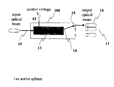
Figure 1 shows the block diagram of an active lxn splitter 100, according to
the present
invention, that is used to route an incident optical beam 10 to one of a
number of egress
optical fibers 11. Using an electrooptic wafer beam deflector component, a
voltage 12 is
applied to the prism segment 13 to produce a deflection angle that determines
the exit
point of the optical beam 14. As shown in [Li 1996] the deflection angle is
proportional
to the applied voltage. A collimator 15 is placed so that it directs the
exiting optical beam
to a corresponding optical fiber 16.
The system in Figure 1 is used as a 1x2 splitter by applying a voltage control
signal that
is either 0 volts or V volts. The time to switch the optical beam from one
position to the
other position can be made very small because of the binary nature of the
control signal.
Figure 2 shows how a lx2m active splitter 200 can be formed by concatenating
in a
substrate multiple prism segments 20, each under an independent binary control
signal
21. The binary nature of the independent control signals enables the 1x2"'
splitter to have
fast transition times.
Figure 3 shows an nxl active combiner 300 which takes a single optical signal
that
arrives at one of n possible input optical fibers 30 and directs it to the
single output fiber
33. A consequence of the reciprocity principle [Stern 1999 pp 228] is that an
active
combiner is obtained by operating an active splitter in reverse. A single
optical signal
arnves in one of n input fibers 30 and is incident at the substrate at a
certain point 31. A
voltage signal 32 then directs the signal to the single output fiber 33. An
active
combiner is more efficient than an ordinary passive combiner in directing the
energy in
the optical beam to the output fiber [Spanke, 1987].
4
CA 02310853 2000-06-06
Figure 4 shows a 4x4 example of an nxn basic switching unit 400 constructed
using n 1 xn
active splitters 200 and n nxl active combiners 300. A single output fiber 40
from each
active splitter is connected to an input 41 of each of the active combiners.
The control
voltage 42 in each active sputter directs the input optical signal to the
desired output fiber
40 and thereafter the optical signal propagates to the corresponding active
combiner. The
active combiner directs the single arriving optical signal to the output fiber
45 under the
control of a voltage signal 46.
A consistent set of control voltage signals is required in the nxn basic
switching system in
Figure 4 to direct each of the n input optical signals to a distinct set of n
output ports.
The nxn basic switching unit is then equivalent to a crossbar switch in the
sense that it
can direct any of n input signals to any output port that is not already in
use.
Figure 5 shows a 4x4 example of an nxn basic switching unit 500 constructed
using n lxn
active splitters 200 and n nxl passive combiners 350. A single output fiber 50
from each
active sputter is connected to an input 51 of each of the active combiners.
The control
voltage 52 in each active sputter directs the input optical signal to the
desired output fiber
53 and thereafter the optical signal propagates to the corresponding passive
combiner.
The passive combiner combines all arnving optical signals and a portion of the
energy in
the arriving optical signal appears at the output fiber 55. The system in
Figure 5 provides
an acceptable basic switching unit as long as the output signals have an
adequate signal-
to-noise ratio.
Benes formulated a general method for constructing large switching fabrics
from smaller
switching fabrics [Hui 1990 pg. 72]. Figure 6 shows an example of how a 16x16
optical
switching fabric 600 can be constructed from three stages of 4x4 basic optical
switching
units 61. Each stage in this Benes construction consists of 4 rows of
individual 4x4 basic
switching units. The ith output fiber 62 from the jth switching unit 63 in the
first stage is
connected to the jth input 64 of the ith basic switching unit 65 in the second
stage. The
interconnection pattern between the second and third stages is the reflection
of the
interconnection pattern between the first and second stage: the ith input
fiber 66 into the
jth switching unit 67 in the third stage is connected to the jth output 68 of
the ith basic
switching unit 69 in the second stage. More generally, given an nxn basic
switchin~ unit
constructed as shown in Figure 4 or in Figure 5, it is possible to construct
and n2 x n
larger switching fabric using a three-stage construction using the
interconnection
approach described above. In general an n2 x n2 three-stage Benes construction
requires
3n basic switching units.
A five-stage n3 x n3 Benes construction for a large switch is obtained as
follows. The
first stage consists of n2 rows of nxn basic switching units. The center stage
consists of n
"central" switches of dimenstion n2 x n2, with the ith output from the jth
basic switch in
the first row connected to the jth input of the ith switch in the second
stage. Moreover,
each n2 x n2 central switch can in turn be decomposed into a three-stage array
of n rows
of nxn basic unit switches. In general an n3 x n3 five-stage Benes
construction requires
CA 02310853 2000-06-06
5n2 basic switching units. More generally, an n'' x nk (2k-1)-stage Benes
construction
requires (2k-1)nk-1 basic switching units.
A preferred embodiment of the present invention involves the construction of
n2 x n2 and
n3 x n3 Benes constructions of optical switching fabrics using the basic nxn
switching
units shown in Figure 4 and Figure 5. The corresponding three- and five-stage
switches
are feasible because of the low loss property of the basic switching units
constructed
using electrooptic wafer beam deflector components.
The Benes method also allows the construction of large optical switching
fabrics from
smaller basic switching units of several sizes. Figure 7 shows a three-stage
16x16
optical switch fabric 700 constructed from first and third stages consisting
of 8 2x2 basic
switching units 71 and a central stage consisting of 2 8x8 basic switching
units 72. In
general, an N=mn switch can be constructed in three stages using first and
third stages of
m nxn basic switching units and a central stage of n mxm basic switching
units. Five-
stage Benes constructions of dimension N=mnk, where m, n, and k are positive
whole
numbers. The first and last stages are constructed using mn kxk basic
switching units;
the Benes method is the applied to each of the k mn x mn central switching
units.
A preferred embodiment of the present invention involves the construction of
three and
five stage Benes optical switching fabrics of dimension N=mn or N=mnk using
basic
switching units shown in Figure 4 and Figure Sof sizes n x n, m x m, and/or k
x k. The
corresponding three- and five-stage switches are feasible because of the low
loss property
of the basic switching units constructed using electrooptic wafer beam
deflector
components.
All the Benes switch fabric constructions described above are "non-blocking"
in the
sense that they can realize any interconnection pattern of any N inputs to any
N distinct
outputs [Hui 1990 pg 70]. The addition of a new connection to an existing set
of fewer
than N existing connections may require the re-arrangement of all connections.
For this
reason Benes switching fabrics are said to be rearrangeably non-blocking.
Various
algorithms have been developed for determining the pattern of interconnections
within
each basic switching units to realize a given overall interconnection pattern
in a Benes
networks [Paull 1962], [Opferman 1971]. Figure 8 shows an example of a
switching
fabric and its associated fabric control unit. The figure only shows the basic
switching
units and their associated control signals. Requests for interconnection
patterns are
received from elsewhere in the system. The connection matrix request pattern
is
examined by the fabric control and an algorithm is executed to determine the
interconnection pattern within the basic switching units in the overall
switching fabric
required to realize the given request pattern. A set of digital control
signals c;~ is then
applied to the ij basic switching unit to execute the desired interconnection
patterns.
These control signals are converted to voltage levels that cause the optical
beams in each
basic switching unit to be routed to the appropriate output. The requested
interconnection
pattern is maintained as long as is necessary by applying the appropriate
control voltage
signals.
6
CA 02310853 2000-06-06
[Clos 1953] developed a method for constructing non-blocking multi-stage
fabrics that do
not require rearrangement of existing connections when a new connection is set
up. The
basic Clos construction for an N=pk switch consisting of three-stages. The
first and
third stages consist of k rows of pxm basic switching units, and the central
stage consists
of m k x k basic switching units. The ith output of the jth switch in the
first row is
connected to the jth input of the ith central switch. It is well-known that if
m=2p-1, then
the Clos fabric is strictly non-blocking in the sense that existing
connections do not need
to be rearranged to establish a new connection from an available input to an
available
output. Figure 9 shows an example of an 8x8 non-blocking Clos switch 800
constructed
from 2x2 and 4x4 basic switching units. In this example, p=2, k=4 and m=2p-
1=3.
A pxm basic switching unit can be constructed by simply using p of the inputs
in an m x
m basic switching unit. A preferred embodiment of the present invention is a
three-stage
arrangement of a Clos switching fabric in which the basic switching units are
constructed
using electrooptic wafer beam deflector components.
The electrooptic wafer beam deflector component can route optical signals and
maintain
high signal quality even when the optical signals are composite and consist of
multiple
wavelength signals. Consequently, the above disclosed optical switches
constructed
using electrooptic wafer beam deflector components have the capability of
transferring
composite optical signals. Figure 10 shows the use of WDM multiplexers and
demultiplexers to concentrate multiple optical signals that occupy non-
overlapping
wavelengths into a single optical signal that can be switched across the NxN
optical
switch. The structure of the switch constrains all components of the composite
signal to
be switched to the same output port. T'he composite signal can then be either
decomposed into individual components, or the entire composite can be
transmitted from
the switch and onto an outgoing optical transmission link.
7