Note : Les descriptions sont présentées dans la langue officielle dans laquelle elles ont été soumises.
CA 02311902 2000-OS-26
Fine projection structure and
Method for Manufacturing the Same
Technical Field
The present invention relates to a fine projection
structure having a fine projection consisting of a solid
solution of semiconductor-metal of nanometer size and a
method for manufacturing the same.
Background Art
A degree of integration of semiconductor devices
typical in DRAMS is yearly increasing. For instance, the
degree of integration of a DRAM has been increased from 16
Mbit to 64 Mbit or 256 Mbit, further being on the increase to
Gbit. Such a high integration of semiconductor devices is
achieved due to a reduction of a unit device size down to
sub-micron order. In developing the finer unit device size,
progress in lithography technology has contributed largely.
In addition to the progress of lithography technology, an
improvement of element structure is also in progress.
As to the lithography technology, exposure technology
with KrF excimer laser, which is conformable to 0.25 a m rule,
is developed. With this technology, 64 Mbit-DRAMS are in
mass production and 256 Mbit-DRAMS are in progress in a
practical application. Further, the exposure technology with
the KrF excimer laser is in improvement to conform to 0.15 a
m rule and exposure technology with SOR light or the like is
being in progress. However, with the existing lithography
1
CA 02311902 2000-OS-26
technology, approximately 0.1 ~cm rule is considered to be a
limit. Accordingly, to achieve further higher integration,
it is desired to realize in the future a unit device size of
namo-meter order.
Further, a device of quantum size, as a candidate for
the future LSI technology, is highly expected. For instance,
there are quantum-wire and quantum-box devices that make use
of wire and box structures respectively of which cross
sections are comparable with a quantum mechanical wavelength
of an electron, and a resonant-tunneling effect device and
resonant tunnel element that make use of a quantum well.
Thus, by utilizing a quantum size effect and quantum tunnel
effect, new devices are tried to be realized.
In order to positively utilize a quantum effect to
develop a new device, it is important for a characteristic
dimension of a device not to stay in the order of phase
wavelength (0.1 to 1 ~cm), that is in a mesoscopic region,
but to be reduced to the order of electron wavelength (10 to
100 mm), that is nanoscopic region. Further, to make more
effective use of the quantum effect device, the unit device
size itself is necessary to be ultra-fine such as, for
instance, 10 to 100 mm. However, the existing lithography
technology can not realize such a device size with stability.
Further, when considering a practical device structure,
after realizing the aforementioned unit device size of
manometer order, bonding state between a conductive layer
that is used as various kinds of functional layers and a
semiconductor substrate has to be stabilized. When a
2
CA 02311902 2000-OS-26
conductive layer of manometer order functions as for instance
an electrode layer, excellent bonding state between an
electrode layer and a semiconductor substrate is necessary to
be realized. However, simple disposition of the conductive
layer of such a size on the semiconductor substrate can bring
about excellent bonding state and more excellent connecting
state with a great difficulty.
As mentioned above, study and development of
semiconductor devices of ultra-high integration and quantum
size devices highly expected as a future candidate of LSI
technology are in progress. To realize such ultra-fine
devices, the unit device size of manometer order is necessary
to be attained with stability. From these circumstances,
ultra-fine technology enabling to attain the unit device size
of manometer is in demand. Further, when considered a
practical device structure, bonding and connecting states
between the conductive layer and the semiconductor substrate
are necessary to be stabilized.
The object of the present invention is to provide a
fine projection structure and a manufacturing method thereof.
The fine projection structure enables to realize a unit
device size demanded in for instance semiconductor devices of
ultra-high integration and quantum size devices and to
stabilize, in such a device size, bonding and connecting
states between a conductive layer and a semiconductor
substrate.
Disclosure of the Invention
3
CA 02311902 2003-05-27
A fine projection structure c~f the pr~,ser.t invention
comprises a semicondu~;:tor substrate, an:l a f ire projection
of a maximum diameter of 500 nm «C: less consisting
essentially of a solid soluticsrr bE-~twcen a -:can~;tituent
element of the semiconductor s'_rl~st.rata~ :end metal and to.rmed
selectively at an arbitrary position on a =surface of the
semiconductor substrate with ~;a:rt therec~f~ Larecip.itating in
the semiconductor substrate.
More specifically, the pz-eser7t inventa c>n provides a
fine projection structure, ._~.ompri;..irrc.~ a serniconductar
substrate including Si and having a flat- surface, and a fine
projection of a maxs.rnum diarnet:c~r r:~f .'>>0~) rErr~ c:.:c Less
consisting essentially of a scl:i_c.~ sol.ut io.n between the Si
which is a constituent: element. c.~f r_rle ;F.~rrric-onductor
substrate and a metal. of at least one sef.ecv.ed from Au, Ag
and Cu, and formed protrusively and selc=:ct__vely at an
arbitrary position on the f:l.at :m.arface ~:vf the semiconductor
substrate, a part of the fine projecti.oln penetrating into
the semiconductor substrate.
The present invention also provides a method for
manufacturing a fine ~>roject ior~ ~atructure, ~:omprising the
steps of disposing on a flat: sum°fac:r t-:f. ~~ scerni.c:ondu.ctcr
substrate including Si a fi.n.e part.:i~cle of a metal of at least
one selected from Au, Ag and t~.r_i, form.i.tng a :overing layer on
the surface of the semiconductor substxai~e caith the exception
of a position where the fine p,~rt.ic::le c:>f me~:a.l is disposed,
and heating the semiconductor :r.abst.rate having the fine
particle of metal in a vacuum atrr~c.~sphere to a temperat~.~re
higher than that where the S:i y:~tc.~m~;and the constituent:
CA 02311902 2003-05-27
atoms of the fine particle of metal dissc:7:Lue d~z~, to
interdiffusion through are irat:c~~x~fa~e tlm=:reoi- tc> form a fine
projection of a maximum r~:i_arr~el:::E-:r ~>f 'lU0 nrn cr less
consisting essentially of a sc~l id sc~llzt i.on between the Si
which is the constituent_ elemE-ant: ~~;~f. t.lre se~ni.conduct.or
substrate and the constituent elerrcea~t:. ~~;f t.,7e tine particle
of metal, a part of thre fine 1>rojection penetrating into the
semiconductor substrate.
In the present f i.ne proje:>c.t:i~:_>n st_r~..rct~zre, the fi~~e
projection consists of a so:Li<:i :=;ul.uti.cw-r beivween for instance
a constituent element of the ~~;emi.~:~:.->ndtz~~t:or substrate and a
metal dissolving the constituent.- ~~~leme.rz(v os: the
semiconductor substrate at hic~'r~ t,:emperG~~~ur~:=s. As an
applicable semiconductor subst raat~e ,Vznd n~-~tr~:l., a combination
of which primary solubili.t:.y l.imi.t. at. a i.k:ermodynamicaLly
high temperature reg:i::m :is l.azrgc= and sc~ i ub:l i t.y _Lirnit at
room temperature regimen der_rea,~;es l.arge~y s rzsed.
Accordingly, during h~ at t:rf~at:ment t::he =~ol:'~, d solution based
on the large solubility limit: <--.~t: ~Lri.gh t.,ery;exature rF,g:i_on
is formed, and as <~ fine projec:t~ic>n in ,r t final state t:hc~
solid solution based an the so:lub~il_ity i_im:i.t of the
semiconductor and metal at: morn t~~,:mperat.rz.rc~ .region is
obtained.
In the present fine project:ic:;n str~~aca:rise, part of a
surface of the semiconductor ~~u~>strate, wit_to the exception
of the fine project~io3i thereon, is :_:o-vowed :by a layer.
In the present fine proje~~tioru :at:z~rzc:tt_az-~>, ~~ rnaximu~m
diameter of a fine ~>rr.:~ject:i~:an ~.~:~~r loc-' i iI~c-. ~ u:~t~ as
v e1
CA 02311902 2000-OS-26
500 nm or less. The size of the fine projection is
particularly preferable to be in the range of 20 to 50 nm.
A method for manufacturing a fine projection of a
maximum diameter of 500 nm or less structure of the present
invention comprises the steps of disposing, on a surface of a
semiconductor substrate, a fine particle of a metal; forming
a covering layer; and heating in a vacuum atmosphere the
semiconductor substrate having the fine particle of metal.
The fine particle of metal is capable of dissolving
constituent atoms of the semiconductor substrate at high
temperatures. The covering layer is formed on the surface of
the semiconductor substrate thereon the fine particle of
metal is disposed with the exception of the position where
the fine particle of metal is disposed. The semiconductor
substrate having the fine particle of metal is heated in a
vacuum atmosphere to a temperature higher than that where the
constituent atoms of the semiconductor substrate and the
constituent atoms of the fine particle of metal dissolve due
to interdiffusion through an interface thereof to form a fine
projection consisting of a solid solution of the constituent
atoms of the semiconductor substrate and the constituent
atoms of the fine particle of metal.
In the present method for manufacturing a fine
projection structure, for the covering layer for instance an
oxide film on a surface of a semiconductor substrate can be
used. In the present method for manufacturing a fine
projection structure, a maximum diameter of the fine particle
of metal is preferable to regulate at 1 a m or less, further
5
CA 02311902 2000-OS-26
at 200 nm or less.
In the present invention, for instance the
semiconductor substrate covered by a layer with the exception
of a position where the fine particle of metal is disposed
undergoes heat treatment at a temperature. The temperature
is higher than that dissolves mutually the constituent atoms
of the semiconductor substrate and the constituent atoms of
the fine particle of metal. During the heat treatment, the
semiconductor substrate and the fine particle of metal form a
solid solution based on interdiffusion through only the
interface thereof.
In this case, the primary solubility limit between the
semiconductor substrate and the fine particle of metal is
large and the semiconductor atoms are prevented from
diffusing through other than an interface between the
semiconductor/metal. Accordingly, metallic atoms diffuse.
into the semiconductor substrate side to form a solid
solution with part of the fine particle of metal
precipitating in the semiconductor substrate. Upon cooling
from this state to a room temperature region, an excess of
semiconductor atoms is excluded from the solid solution.
Thereby, a fine projection consisting of a solid solution
between the semiconductor and the metal based on the
solubility limit at room. temperature region is obtained.
Further, the fine projection consisting of the
semiconductor-metal solid solution, a state during heat
treatment being nearly maintained, is formed in the form of
part thereof precipitating in the semiconductor substrate.
6
CA 02311902 2000-OS-26
The fine projection of the present invention is formed due to
self-organizing mechanism, being able to form according to
the size and a position of disposition of the initial fine
particle of metal.
According to the present fine projection as described
above, conforming to the initial size of a fine particle of
metal, a unit device size (for instance a single electron
device) of manometer order can be realized. Further, in such
a device size, bonding state and connecting state between the
fine projection as for instance a conductive layer and a
semiconductor substrate can be stabilized.
Brief Description of the Drawings
Figs. 1A, 18 and 1C are diagrams showing schematically
one embodiment of steps of manufacturing a fine projection
structure of the present invention and the fine projection
structure obtained thereby, and
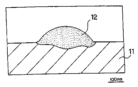
Fig. 2 is a diagram showing schematically a result of
TEM observation of a fine projection structure manufactured
2.0 according to embodiment of the present invention.
Modes for Implementing the Invention
In the following, modes for carrying out the present
invention will be explained.
Figs. 1A to 1C are diagrams showing schematically one
embodiment of manufacturing steps of a fine projection
structure of the present invention. In manufacturing a fine
projection structure of the present invention, first as shown
7
CA 02311902 2000-OS-26
in Fig. 1A, a fine particle of metal 2 is disposed on a
semiconductor substrate 1. For the semiconductor substrate,
Si substrate, Ge substrate, GaAs substrate or multi-layered
substrate thereof can be used.
Here, for the semiconductor substrate 1 and the fine
particle of metal 2, a combination showing a
thermodynamically endothermic reaction, that is, one of which
solubility limit, though large at a high temperature region,
largely decreases at room temperature region can be used.
For instance, when Si substrate is used as the
semiconductor substrate 1, for constituent material of the
fine particle of metal 2, Au, Ag, Cu and A1 can be cited.
Among these, particularly Au, Ag and Cu large in diffusion
coefficient to Si are preferably used. Due to the use of
these metals, a fine projection 4 part of which precipitates
in the semiconductor substrate 1 and that will be described
later in detail can be obtained with ease. Further, when a
Ge substrate is used as the semiconductor substrate 1, as
constituent material of the fine particle of metal 2, Zn, Cd,
Au, Ag and A1 can be used.
Further, when an oxide film on the surface of the
semiconductor substrate 1 is applied as a covering layer 3
that will be described later, so as to prevent the fine
particle of metal 2 from being oxidized during formation of
the oxide film on the surface, for the constituent material
of the fine particle of metal 2, metals difficult to oxidize
such as Au and Ag can be preferably used.
In forming the fine particle of metal 2, a surface of
8
CA 02311902 2000-OS-26
the semiconductor substrate 1 is sufficiently cleaned. On
such a surface of the semiconductor substrate 1, for instance
under reduced pressure or a vacuum, the fine particle of
metal 2 is formed.
Though a method for forming the fine particle of metal
2 is not particularly restricted, a method capable of forming
the fine particle o.f metal 2 on the semiconductor substrate
at a room temperature state is applied. When a fine particle
of metal 2 is formed on the semiconductor substrate 1 that is
heated, a reaction layer or the like is formed at an
interface between the semiconductor substrate 1 and the fine
particle of metal 2 to be likely to affect adversely on the
subsequent steps. As a specific method for forming the fine
particle of metal 2, for instance gas-phase condensation
method, molecular beam epitaxy method (MBE method) or the
like can be cited.
The size of the fine particle of metal 2, as will be
described later, needs only to be one of which degree enables
the constituent elements of both the semiconductor substrate
1 (for instance Si atoms) and the fine particle of metal 2 to
interdiffuse through an interface therebetween to form a
solid solution of semiconductor-metal.
In specific, a maximum diameter of the fine particle of
metal 2 is preferable to be 1 a m or less, being further
preferable to be 200 nm or less. The size of the fine
particle of metal 2 is desirable to be made so as to enable
to obtain a fine projection 4 of a size of approximately 20
to 50 nm in particular. When the size of the initial fine
9
CA 02311902 2000-OS-26
particle of metal 2 is too large, in the courses of formation
and heat treatment thereof, at an interface between the
semiconductor substrate 1 and the fine particle of metal 2, a
layer of reaction or the like is formed to be liable to
affect adversely on the subsequent steps. Further, a dot
capable of confining an electron can not be obtained.
Next, as shown in Fig. 1B, on a surface of the
semiconductor substrate 1 thereon a fine particle of metal 2
is disposed, with the exception of a position where the fine
particle of metal 2 is disposed, a covering layer 3 is formed.
The,covering layer 3, in the subsequent heat treatment step,
in the courses of raising the temperature up to a heat
treatment temperature and maintaining it at the treatment
temperature, prevents the constituent atoms of the
semiconductor substrate 1 from diffusing on a surface thereof
1. However, when atomic diffusion occurs through the
covering layer 3, the covering layer 3 can be disposed on the
entire surface of the semiconductor substrate 1. In this
case, after forming a semiconductor-metal solid solution, the
covering layer 3 functions as an electron barrier layer.
Thus, by suppressing surface diffusion of the
semiconductor substrate l, semiconductor atoms are restricted
in supply to the fine particle of metal 2. Thereby, in the
step of heat treatment, the constituent atoms of the
semiconductor substrate 1 and those of fine particle of metal
2 interdiffuse through only the interface therebetween.
For the covering layer 3, if possible suppressing the
surface diffusion of the semiconductor substrate l, various
CA 02311902 2000-OS-26
kinds of materials can be used. For instance, the oxide film
on the surface of the semiconductor substrate 1, being easy
to form and capable of effectively suppressing the surface
diffusion, is preferably used as the covering layer 3.
The oxide film on the surface of the semiconductor
substrate 1 as the covering layer 3, after disposing in a
vacuum the fine particle of metal 2 on the semiconductor
substrate 1, can be easily formed by exposing once the
semiconductor substrate 1 to air. The oxide film on the
surface as the covering layer 3 needs only to have such a
thickness as capable of suppressing the surface diffusion of
the semiconductor substrate 1, being enough to have for
instance a thickness of approximately 10 nm or less.
Next, the semiconductor substrate 1 thereon the fine
particle of metal 2 is disposed undergoes heat treatment in a
vacuum atmosphere at a temperature higher than that where the
constituent atoms of both the semiconductor substrate 1 and
the fine particle of metal 2 interdiffuse to form a .solid
solution thereof. Thus, by heat treating at a temperature
where the constituent atoms of both the semiconductor
substrate 1 and the fine particle of metal 2 interdiffuse to
form a solid solution, under the heat treatment temperature a
semiconductor-metal solid solution can be formed based on the
primary solubility limit at the high temperature region.
In this case, since the surface of the semiconductor
substrate 1 is covered by the covering 3, the surface
diffusion of the semiconductor atoms is restricted.
Accordingly, the constituent atoms of both the semiconductor
11
CA 02311902 2000-OS-26
substrate 1 and the fine particle of metal 2 interdiffuse
through only the interface thereof.
When the semiconductor-metal solid solution is formed
while suppressing the surface diffusion of the semiconductor
atoms, in the course of maintaining the high temperature, the
metallic atoms diffuse toward the semiconductor substrate 1
to form a solid solution with part of the fine particle of
metal 2 precipitating in the semiconductor substrate 1 side.
In the course of cooling, though an excess of semiconductor
atoms is excluded from the solid solution, while nearly
maintaining the shape of the solid solution during the heat
treatment, the semiconductor-metal solid solution based on
the solubility limit at room temperature region is formed.
That is, as shown in Fig. 1C, according to the shape during
the heat treatment, a fine projection 4 consisting of the
semiconductor-metal solid solution based on the solubility
limit at room temperature can be obtained.
Thus, by forming a semiconductor-metal solid solution
based on the interdiffusion through only the interface
between the semiconductor substrate 1 and the fine particle
of metal 2, as shown in Fig. 1C, the fine projection 4
consisting of the semiconductor-metal solid solution based on
the solubility limit at room temperature can be formed in the
form of part thereof precipitating in the semiconductor
substrate 1.
The fine projection 4 consisting of the semiconductor-
metal solid solution is formed based on the initial fine
particle of metal 2. Accordingly, according to the initial
12
CA 02311902 2000-OS-26
size or the like of the fine particle of metal 2, the maximum
diameter of the fine projection 4 can be made 500 nm or less.
The size of the fine projection 4 can be made further finer
such as 300 nm or less. The size of the fine projection 4 is
particularly preferable to be in the range of 20 to 50 nm.
According to the present invention, the fine projection 4 of
such a small size can be obtained.
After forming the fine projection 4 consisting of the
semiconductor metal solid solution, at an interface between
the fine projection 4 and the semiconductor substrate 1, an
electron barrier can be formed. Such a barrier, by
selectively using for instance a material easy in
interfacial-diffusion for the covering layer 3 and diffusing
such the material due to the interfacial diffusion in the
subsequent step after the step of forming the fine projection
4, can be formed.
As, mentioned above, by applying the present
manufacturing method, at an arbitrary position on the surface
of the semiconductor substrate 1, a fine projection 4
consisting of the semiconductor-metal solid solution can be
obtained. Since the size of the fine projection 4 can be
controlled due to the size of the initial fine particle of
metal 2 and the heat treatment temperature, the fine
projection 4 can be obtained as a dot of for instance
nanometer order. Further, by controlling the position of the
disposition of the initial fine particle of metal 2, at an
arbitrary position on the semiconductor substrate 1 a fine
13
CA 02311902 2000-OS-26
projection 4 can be formed.
By using such the fine projection 4 as for instance
various kinds of conductive layers, further as various kinds
of functional layers, for instance single electron devices of
nanometer order can be realized separated. That is extremely
effective in realizing semiconductor devices of ultra-high
integration and quantum size devices. Other than these,
various kinds of ultra-fine devices can be realized.
Further, the fine projection 4 consisting of the
present semiconductor-metal solid solution is formed in a
state of part of the protrusion 4 precipitating in the
semiconductor substrate 1. Accordingly, excellent bonding
state and connecting state between the fine projection 4 as
for instance a conductive layer and the semiconductor
substrate 1 can be realized. That brings about an extremely
large effect in realizing a practical device structure of
such as single electron devices of nanometer order.
Next, specific embodiments of the present invention
will be described.
Embodiment 1
First, a Si (111) single crystal substrate (non-doped,
ao = 0.5431 nm) is prepared: The Si (111) single crystal
substrate, after chemical cleaning, to remove surface oxide
film and to obtain a hydrogen-terminated Si surface, is
dipped in a dilute HF solution (2~ by weight) for 30 seconds.
Thus pre-treated Si (111) single crystal substrate is mounted
in a vacuum chamber with a background pressure of 10'6 Torr
14
i
CA 02311902 2000-OS-26
or better.
Next, on a surface of the Si (111) single crystal
substrate, a fine particle of Au of a diameter of
approximately 200 nm is generated by use of a molecular beam
epitaxy method. Then, the Si substrate thereon the fine
particle of Au is formed, after once taking out in the air
and mounting again in the vacuum chamber, is heat treated
under an atmosphere of a high vacuum of 1 X 10⁻⁸ Torr or
better. At this time, the heat treatment temperature is set
at 800°C.
The structure and the composition of the aforementioned
heat-treated sample are evaluated by the use of a high-
resolution transmission electron microscope (HRTEM) and an
energy dispersive X-ray spectrometer (EDX). As the result of
this, a sectional TEM image of the heat-treated sample is
schematically shown in Fig. 2: From the TEM observation of
the fine particle of Au formed by the use of the molecular
beam epitaxy method, the initial fine particle of Au formed
on the Si (111) single crystal substrate is confirmed to have
a diameter of approximately 200 nm.
As shown in Fig. 2, a fine projection (fine dot) 12 is
confirmed to form on the surface of the heat-treated Si (111)
single crystal substrate 11. Further, the fine dot 12 is
confirmed to form with the part thereof precipitating in the
Si (111) single crystal substrate.
In order to evaluate the composition of the fine dot 12,
EDX analysis is carried out. The EDX analysis is implemented
with an electron beam of a diameter of beam of 5 nm or less.
CA 02311902 2000-OS-26
From the result of the EDX analysis, it is confirmed that
from the portion of the Si substrate 11 below the fine dot 12,
only Si peaks appear, thus even after the heat treatment, the
Si (111) single crystal substrate 11 maintains its state.
On the other hand, from the results of measurements on
the portion of the fine dot 12, peaks of Si and Au are
detected, thus the fine dot 12 is confirmed to consist of a
solid solution between Si and Au. Further, on the surface of
the Si (111) single crystal substrate 11 with the exception
of the portion where the fine dot 12 is formed, an oxide film
is confirmed to form.
Thus, the fine dot 12 consists of a solid solution in
which Si dissolves in Au based on the solubility limit
thereof, though the shape thereof maintaining that of the
initial Au fine particle, part thereof being formed
precipitating in the Si (111) single crystal substrate 11. A
state of solid solution of Si and Au can be controlled to a
homogeneous one or a state having a concentration gradient
due to for instance heat treatment.
The aforementioned dot of Si-Au solid solution is
supposed to form for instance in the following way.
First, a Si substrate thereon a fine particle of Au is
formed is once taken out in the air to oxidize the surface of
the Si (111) single crystal substrate with the exception of
the position of disposition of the fine particle of Au. The
surface of the Si (111) single crystal substrate except the
fine particle of Au, after being covered by an oxide film (a
covering layer), is heat treated under a high vacuum, thereby
16
CA 02311902 2000-OS-26
Si atoms on the surface of the Si substrate being suppressed
in diffusing.
Accordingly, only through an interface between the fine
particle of Au and the Si (111) single crystal substrate, Au
and Si diffuse mutually, based on the interdiffusion a Si-Au
solid solution being formed. By cooling this, an excess of
Si atoms are excluded, based on the solubility limit of Si
and Au at room temperature, a dot of Si-Au solid solution
being formed with the part thereof precipitating in the Si
substrate.
The results due to the embodiment show that a dot of
Si-Au solid solution of which part bites in the Si substrate,
that is, a fine dot of excellent bonding state and connecting
state, can be formed in nanometer scale. The size of a dot
of Si-Au solid solution, being able to control due to the
size of the fine particle of Au, the heat treatment
temperature or the like, can be applied to manufacture of
various kinds of fine devices.
Embodiment 2
On a surface of the Si (111) single crystal substrate
pretreated identical with embodiment 1, an ultra-fine
particle of Au of a diameter of approximately 20 nm is
deposited. The ultra-fine particle of Au is formed by use of
a gas phase condensation method. That is, in an atmosphere
of Ar, Au of purity of 99.99 is evaporated to deposit on the
Si (111) single crystal substrate as an ultra-fine particle.
The ultra-fine particle of Au deposits itself on the Si (111)
single crystal substrate under room temperature.
17
CA 02311902 2000-OS-26
The Si substrate thereon the ultra-fine particle of Au
is deposited is once taken out in the air, being mounted
again in a vacuum chamber, being heat treated under an
atmosphere of a high vacuum of 1 X 10-e Torr or better. The
heat treatment is carried out under the identical conditions
with those of embodiment 1.
When the state of the heat treated sample is measured
and evaluated in the identical way with embodiment 1, as
identical as embodiment 1, a fine projection (a dot of Si-Au
solid solution) is confirmed to be formed of a solid solution
in which Si dissolves in Au based on the solubility limit at
room temperature. It is confirmed that the shape of the dot
of Si-Au solid solution, though the size thereof is a little
bit larger than that of the initial ultra-fine particle of Au,
maintains approximately the initial shape thereof, the part
of which precipitating in the Si (111) single crystal
substrate.
Industrial Applicability
A fine projection structure of the present invention
consists of a solid solution of a constituent element of a
semiconductor substrate and a metal, showing an excellent
bonding state and connecting state to the semiconductor
substrate. Such a fine projection structure largely
contributes in realizing for instance an ultra-high
integration semiconductor device, quantum size device or the
like.
18