Note : Les descriptions sont présentées dans la langue officielle dans laquelle elles ont été soumises.
CA 02314109 2000-06-14
WO 00/22193 PCT/US99/23653
TITLE: ELECTRODEPOSITION OF METALS IN SMALL RECESSES USING
MODULATED ELECTRIC FIELDS
CROSS-REFERENCE TO RELATED APPLICATIONS
This application is a continuation-in-part of copending
applications Serial No. 09/172,299, filed October 14, 19998, and
Serial No. 09/239,811, filed January 29, 1999.
ORIGIN OF THE INVENTION
The experimental work leading to this invention was funded
in part by U.S. Air Force Materials Command Contract No. F33615-
IS 98-C-1273.
BACKGROUND OF THE INVENTION
Field of the Invention:
This invention relates to electrodeposition of metals and
more particularly to electrodeposition of metals into small or
microscopic recesses on the surface of a substrate and formation
of uniform layers of electrodeposited metal on a substrate.
Brief Description of the Prior Art:
Electronic devices such as computers, cellular telephones,
electronic entertainment devices, and the like, have long been
manufactured by mounting components on circuit boards having
electrically conductive traces thereon to interconnect the
components.
In the manufacture of such electronic equipment,
development of technology and economics have driven the industry
toward ever-smaller devices, containing ever-increasing numbers
of components. At the level of semiconductor devices very large
scale integration (VLSI) has produced chips containing up to a
few million transistors on a single semiconductor chip no larger
- 1 -
CA 02314109 2000-06-14
WO 00/Z2193 PCT/US99/23653
than several millimeters on a side. Such chips have
conventionally been packaged or encapsulated in small modules
having external lead wires for interconnecting the chips. The
interconnections have conventionally been provided by circuit
boards having electrical conductors prepared by so called
"printed wiring" techniques that involve masking, etching, and
plating of conductive metal, usually copper, to provide the
interconnects between chip modules or sockets designed to hold
such modules. These "printed wiring boards" (PWB) have
l0 typically been used to interconnect chips of conventional sizes.
The chips or socket are mounted on the surface of the board with
terminals fitted into holes through the board. The holes are
typically lined with a thin layer of copper that is integral
with the traces of copper on the surface of the board. The
terminals of the chips or sockets are soldered to the copper
layer lining the holes and thereby interconnected through the
copper traces. The PWBs may have more than one layer of copper
traces. Connections between traces in different layers are also
provided by copper-lined holes passing through the board,
commonly known as plated through-holes (PTHs).
The copper lining in such holes is typically applied
electrolytically, by first laying down a thin layer of
electroless copper to provide electrical continuity and then
electroplating copper to a thickness of a few mils to provide
the connecting layer. The holes in the PWBs typically are at
least 12-13 mils in diameter. Because of the well-known problem
of depositing metal electrolytically in recesses, special
techniques have to be used to assure that a uniform layer of
conductive metal is deposited in the holes. Consequently
conventional techniques to enhance the "throwing power" of the
electroplating system have been employed, such as agitation of
the bath, addition of certain chemical compounds to the
electroplating bath, and/or the use of pulsed current plating.
Although conventional techniques have generally been
successful in the manufacture of PWBs having the dimensions that
- 2 -
CA 02314109 2000-06-14
WO 00/22193 PCTNS99/23653
have been commonly used in electronic devices such as television
receivers, personal computers, and the like, the trend to ever-
smaller equipment such as cellular telephones, more advanced
computers, and the like, has led to the necessity of mounting
chips closer together in multichip modules (MCMs). Instead of
terminals extending into holes in the circuit board, such MCMs
frequently have only metallized locations on a major surface of
the module to provide interconnections. The semiconductor
devices or chips are placed relatively close together on a
l0 substrate having holes drilled therein at the locations of the
interconnecting pads on the modules. In such boards the holes
are typically of smaller diameter than those of conventional
PWBs, and may range from about 25 micrometers (1 mil) to about
250 micrometers (10 mils). Such holes are also effectively
blind holes, because the semiconductor devices are already
mounted to the board, and the conductor deposition step provides
the electrical contact to the terminal pads on the semiconductor
devices as well as the interconnections between the devices.
The use of small chips mounted close together and interconnected
by means of conductors deposited in small holes has come to be
known as high density interconnect (HDI) technology. With single
sided, double sided and multilayers representing the first three
generations of PWBs, high density PWBs are also being termed the
fourth generation PWB. Other names for this emerging technology
includes build up boards and micro via boards.
Deposition of conductive metal into the small, blind holes
or vias used in HDI has presented a number of problems.
Conventional metallization procedures, such as chemical vapor
deposition or physical vapor deposition or electroless plating,
are slow and expensive. Electroplating into small blind holes
using conventional procedures has not been able to provide a
reliable layer of conductive metal in the hole to assure a
reliable interconnection of the chips. In particular,
conventional electroplating techniques tend to deposit excess
metal at the sharp corners at the top or entrance of the hole.
- 3 -
CA 02314109 2000-06-14
WO OO/Z2193 PCT/US99/23653
Such deposits encroach on the opening of the hole and hinder
deposition in the lower portion of the hole. They may even
completely block the mouth of the hole leading to voids in the
vias or interconnects. Additionally, in some cases it is
desirable to obtain a conformal deposit, which is also adversely
affected by dogboning at the corners of the vias. Furthermore,
chemical additives in the plating bath may lead to inclusions of
impurities derived from the plating bath within the metal
deposit. Such problems can lead to connections that have a high
electrical resistance and are mechanically brittle and
unreliable in service. In addition, the use of nonconventional
electroplating techniques such as pulse current plating,
typically in conjunction with chemical additives, has relied on
waveform parameters successfully developed for traditional PWB
applications, such as 13 mil and greater PTHs. These waveforms
generally operate with long cathodic duty cycles and short
anodic duty cycles. This approach has led to similar problems
encountered in conventional plating with excess metal deposit at
the opening of the via leading to voids in the interconnect or
to excessive deposit of metal on the surface of the substrate.
In addition to the problems cited above, such nonuniform
metallization within the via or between the via and the
substrate results in excessive processing time and cost
associated with the excess metal.
Similar problems regarding the electrodeposition of
metallic conductors are encountered in the manufacture of the
semiconductor devices themselves that are mounted on the circuit
boards and interconnected by conductive traces.
The manufacture of semiconductor devices, especially very
large scale integrated (VLSI) as well as ultra large scale
integrated (ULSI) chips is driven by technical and economic
considerations toward the production of devices comprising
greater numbers of transistors and associated circuits on a
single semiconductor chip or wafer. For clarity, VLSI is meant
to include both VLSI and ULSI chips. The most complex chips
- 4 -
CA 02314109 2000-06-14
WO 00/22193 PCT/US99l23653
manufactured today have a few million transistors on a
semiconductor chip no larger than several millimeters on a side.
The electrical interconnections between the transistors in such
chips are provided by fine wires of a conductive metal extending
in channels formed horizontally and vertically in the body of
the chip. Conventionally, these electrical connections have
been made of aluminum, which can be deposited through vapor
phase deposition techniques such as physical vapor deposition
(PVD) and chemical vapor deposition (CVD). However, as the
l0 dimensions of the transistors have decreased into the submicron
region, the cross sections of the connections have also
decreased and the resistance of the connections has increased.
In order to reduce the resistance of the connections in VLSI
circuits containing devices of submicron dimensions, the use of
copper as a connecting material has come to be favored.
Furthermore, as the dimensions of the interconnections
between the devices have decreased, the use of conductors of
high aspect ratio has become desirable. When VLSI devices are
prepared by the damascene process, which requires that the
conducting metal be deposited into trenches formed in a layer of
insulating material, it has been found difficult to achieve
void-free metal deposits in trenches having high aspect ratios
by PVD or CVD.
Attempts have been made to deposit copper conductors into
trenches on damascene-prepared surfaces by electroplating.
However, it has proved difficult to prepare void-free, and
inclusion-free deposits in trenches of high aspect ratio.
Furthermore, electroplating of copper into trenches of a
damascene-prepared surface has required depositing a relatively
thick layer of copper over the entire surface of the wafer. The
excess copper must then be removed by chemical-mechanical
polishing (CMP), which is a time-consuming process that also
generates substantial amounts of waste slurries that require
careful and expensive disposal procedures.
- 5 -
CA 02314109 2000-06-14
WO 00/22193 PCT/US99/23653
Electroplating has also been used to deposit a thin layer
of copper on the surface of a large semiconductor wafer
preparatory to forming electrical interconnections by the
customary masking and etching procedures. However, because of
the tendency of electroplating procedures to deposit excess
metal at the edges of the wafer, it has proved difficult to
prepare perfectly uniform layers of copper. Auxiliary
electrodes have been used to surround the edges of the wafer in
order to provide a uniform electric field, as disclosed, for
example in U.S. Patent 5,135,636, to Yee et al. However, such
procedures require additional equipment and are evidently
wasteful of copper metal.
Accordingly, a need has continued to exist fox a method of
depositing metals in small or microscopic recesses on a
substrate in a controlled and efficient manner. In particular,
a need has continued to exist for a method of depositing
metallic conductors, especially copper, into small recesses such
as the blind holes used in high density interconnects for
multichip modules and the like and damascene trenches on
semiconductor wafers, as well as for depositing a thin uniform
layer of a metal such as copper over the entire surface of a
semiconductor wafer with minimal need for subsequent
planarization. Fabrication of other microtechnologies such as
micromechanical machines (MEMS) also require metallization of a
small feature followed by planarization.
SUMMARY OF THE INVENTION
The problems encountered in electrodeposition of continuous
conductive layers of metals into small blind holes and vias have
now been alleviated by the method of this invention, wherein a
metal is selectively deposited on a substrate to provide a
coating that lines or fills small blind holes and/or recesses
without excessive deposition of metal at or near convex portions
of the substrate surface such as protuberances and edges. The
selective deposition is accomplished by a process in which an
- 6 -
CA 02314109 2000-06-14
WO 00/Z2193 PCT/US99l23653
electrically conductive substrate having a blind hole, groove,
trench, or other small or microscopic recess with at least one
transverse dimension not greater than about 350 micrometers is
immersed in an electroplating bath containing ions of the metal
to be deposited in said recess, and provided with a suitable
counterelectrode,
and
a modulated reversing electric current is passed through
the plating bath having pulses that are cathodic with respect to
the substrate and pulses that are anodic with respect to the
substrate, the cathodic pulses having a short duty cycle and the
anodic pulses having a long duty cycle, the charge transfer
ratio of the cathodic pulses to the anodic pulses being greater
than one or effectively greater than one when the current
efficiencies of the cathodic and anodic processes are taken into
account, and the frequency of the pulses ranging from about
10 Hertz to about 12 kilohertz.
Accordingly. it is an object of the invention to provide an
electrochemical method for depositing a metal on a substrate
A further object is to provide a method for selective
electrodeposition of a metal on a substrate having small or
microscopic recesses on its surface.
A further object of the invention is to provide an
electrochemical method for depositing, either by filling or by
conformal coating, a metal in small blind holes in a substrate.
A further object is to provide a method for depositing
metal from an electrolytic bath onto a substrate having recesses
therein in order to provide reliable electrical connection
between the surface of the substrate and the bottom portion of
the recess.
A further object is to provide a method for forming a void-
free deposit of metal in a small recess on the surface of a
substrate.
CA 02314109 2000-06-14
WO 00/22193 PCT/US99/23653
A further object is to provide a method for
electrodepositing metal into a small recess on the surface of a
substrate without excessive deposition of metal on the surface
of the substrate.
A further object is to provide a method for depositing
metal from an electrolytic bath onto a substrate while
preventing excessive deposition at corners and protuberances of
the substrate.
l0 Further objects of the invention will become apparent from
the description of the invention which follows.
BRIEF DESCRIPTION OF THE DRAWINGS
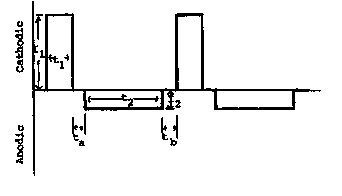
Figure 1 illustrates the waveform of modulated reverse
electric current used in the method of the invention.
Figure 2A illustrates the thickness of the Nernst diffusion
layer with respect to the surface roughness of an electroplating
substrate having a microrough surface.
Figure 2B illustrates the thickness of the Nernst diffusion
layer with respect to the surface roughness of an electroplating
substrate having a macrorough surface.
Figure 2C illustrates the thickness of the Nernst diffusion
layer with respect to a substrate having small recesses having
transverse dimensions of about 5 micrometers to about
350 micrometers and aspect ratios of from about 0.5 to about 5.
Figure 3A is a cross section of a damascene-prepared
substrate having a trench or depression formed in a layer of
insulating material deposited on a semiconductor substrate.
Figure 3B is a schematic representation of the substrate of
Figure 2 after metal deposition by a cathodic pulse.
Figure 3C is a schematic representation of the substrate of
Figures 3A and 3B after a further treatment with an anodic
pulse.
- 8 -
CA 02314109 2000-06-14
WO 00/22193 PCTNS99/23653
Figure 3D is a schematic representation of the substrate of
Figure 3A after a succession of cathodic and anodic pulses,
showing the preferential deposition of metal in the damascene
trench.
Figure 3E is a cross section of the plated substrate of
Figures 3A-3D after the damascene trench has been filled with
metal, showing the filled trench and thin surface layer of
metal.
Figure 3F is a cross section of the plated substrate of
Figure 3E after subsequent processing to remove the thin surface
layer of metal.
Figure 4A is a cross section of a semiconductor wafer
prepared for electrodeposition of a thin, uniform layer of metal
on its surface.
Figure 48 shows one edge of the semiconductor wafer of
Figure 4A, indicated by circle 9B in figure 4A, in an enlarged
view after metal deposition by a cathodic pulse, showing the
excess thickness of metal deposited at the edge of the wafer
with a much exaggerated vertical dimension.
2o Figure 4C shows the edge portion of the wafer edge of
Figure 9B after a subsequent anodic pulse, showing removal of
excess metal near the edge of the wafer, with a greatly
exaggerated vertical dimension.
Figure 9D shows the edge portion of the wafer of
Figures 4A-4C after a succession of cathodic and anodic pulses,
showing the thin, uniform layer of metal extending with a
generally constant thickness to the edge of the wafer.
Figure 5A illustrates a schematic cross-section of a
multichip module showing the connection of one module to another
3o through a vias prepared by the process of the invention.
Figure 5B illustrates a schematic cross-section of a
multichip module having amore than one interconnect layer,
showing the formation of stacked vias prepared by the process of
the invention.
- 9 -
CA 02314109 2000-06-14
WO 00/22193 PCT/US99/23653
Figure 6 is a photomicrograph of a cross section of a
102 micrometer diameter hole in a brass substrate plated with
copper using direct current.
Figure 7 is a photomicrograph of a cross section of a
102 micrometer diameter hole in a brass substrate plated with
copper using pulsed current.
Figure 8 is a photomicrograph of a cross section of a
102 micrometer diameter hole in a brass substrate plated with
copper using modulated reverse electric fields at a relatively
l0 low frequency of 98.13 Hz with a long cathodic duty cycle and a
short anodic duty cycle.
Figure 9 is a photomicrograph of a cross section of a
102 micrometer diameter hole in a brass substrate plated with
copper using modulated reverse electric fields at a relatively
high frequency of 2618 Hz with a long cathodic duty cycle and a
short anodic duty cycle.
Figure 10 is a photomicrograph of a cross section of a
102 micrometer diameter hole in a brass substrate plated with
copper using modulated reverse electric fields at a relatively
high frequency of 3413 Hz with a short cathodic duty cycle and a
long anodic duty cycle for a period of time to plate a thin
continuous layer of copper over the surface of the substrate and
the interior surface of the hole.
Figure 11 is a photomicrograph of a cross section of a
102 micrometer diameter hole in a brass substrate plated with
copper using modulated reverse electric fields at a relatively
high frequency of 3413 Hz with a short cathodic duty cycle and a
long anodic duty cycle for a period of time to plate a thin
continuous layer of copper over the surface of the substrate and
to fill the interior of the hole.
Figure 12 is a photomicrograph of a cross-section of
trenches on the surface of a silicon wafer filled by
electrodeposition of copper according to Example 7.
- 10 -
CA 02314109 2000-06-14
WO 00/22193 PCT/US99/23653
Figure 13 is a photomicrograph of a cross-section of
trenches on the surface of a silicon wafer filled by
electrodeposition of copper according to Example 8.
Figure 14 is a photomicrograph of a cross-section of
trenches on the surface of a silicon wafer filled by
electrodeposition of copper according to Example 9.
Figure 15 is a photomicrograph of a cross-section of
trenches on the surface of a silicon wafer filled by
electrodeposition of copper according to Example 10.
Figure 16 is a photomicrograph of a cross-section of
trenches on the surface of a silicon wafer filled by
electrodeposition of copper according to Example 11.
Figure 17 is a photomicrograph of a cross-section of
trenches on the surface of a silicon wafer filled by
electrodeposition of copper according to Example 12.
DETAILED DESCRIPTION OF THE INVENTION AND PREFERRED EMBODIMENTS
The distribution of metal electrodeposited on an
electrically conductive substrate is determined by the local
variations in the electrical current density. The primary
current distribution in an electroplating cell is determined by
the geometry of the electrodes. Typically, the primary current
density is inversely proportional to the distance between the
cathode and the anode along the path that the current follows
between the electrodes.
When a voltage is first applied to the electroplating cell,
the metal ions in solution in contact with the cathode are
deposited on the cathode and the concentration of the ions in
the adjacent solution decreases. Consequently, a concentration
gradient is established near the cathode, and metal ions
accordingly diffuse from the bulk solution region of relatively
high concentration toward the depleted region adjacent to the
cathode. This layer of depleted and variable metal ion
concentration is the Nernst diffusion layer. In direct-current
(DC) electroplating, the Nernst diffusion layer will rapidly
- 11 -
CA 02314109 2000-06-14
WO 00/22193 PCT/US99/23653
reach a steady-state thickness that is determined by the current
density and the degree of agitation of the bath which produces a
relative motion of the bulk electrolyte with respect to the
electrode (8N,oc in Figures 2A, 2B and 2C). The more vigorous the
agitation of the electrolyte in the plating bath, the thinner
the Nernst diffusion layer will be. However, even for very
vigorous relative motion between the bulk electrolyte and the
electrode, e.g., with use of a rotating disk electrode, the
thickness of the Nernst diffusion layer will still amount to
l0 several micrometers.
The substrate surface will not, in general, be perfectly
smooth. If the roughness of the surface, i.e., the size of the
peaks and valleys therein, is large compared with the thickness
BN,oc of the Nernst diffusion layer (a "macrorough" surface), the
layer will tend to follow the surface asperities, as shown in
Figure 2B. Under these circumstances the electric field which
determines the primary current distribution will be greater at
the tips of the asperities than in the valleys. Accordingly,
electrochemical reduction, i.e., deposition of metal, will take
place preferentially at the peaks. The current flow in the
electrolyte will establish a somewhat greater overpotential in
the depressions of a macrorough surface than at the peaks, which
will tend to provide a secondary current distribution that still
favors metal deposition at the peaks, although perhaps not as
much as the primary current distribution.
Figure 2B indicates that, on a macrorough surface, the
Nernst diffusion layer follows the contour of the surface
asperities. Accordingly, the distribution of electrodeposited
metal is not greatly affected by microvariations in current
distribution caused by microasperities, as is the case for
microrough substrates, as illustrated in Figure 2A and discussed
below. Therefore the thickness of the metal deposit on the
peaks and valleys of a macrorough surface is determined
essentially by the primary and secondary current distribution.
- 12 -
CA 02314109 2000-06-14
WO 00/22193 PCT/US99/23653
In conventional electroplating of industrial objects, the
dimensions of any surface features are large with respect to the
thickness of the Nernst diffusion layer. This relationship
extends even to relatively small articles such as printed
circuit boards, where the smallest features, e.g., through-
holes, typically have dimensions of the order of 10-15 mils.
In electroplating of substrates having surface features
significantly smaller than the Nernst diffusion layer, such as
semiconductor wafers, the diffusion layer when plating is
conducted using direct current (DC) not follow the microscopic
peaks and valleys of the surface, as illustrated in Fig. 2A.
For such "microrough" surfaces, the current distribution will
also favor the deposition of metal at the peaks of the
asperities, once the diffusion layer is established, because the
IS concentration of metal ions, as determined by their rate of
diffusion from the bulk phase, will tend to be slightly greater
at the peaks. Such a current distribution is generally referred
to as the tertiary current distribution.
When the substrate has a relatively smooth surface with
trenches or holes therein having a transverse dimension in the
range of from about 5 micrometers to about 350 micrometers, the
relationship of the Nernst diffusion layer to the surface
profile is more complex, and predictions regarding the behavior
of the electrochemical deposit are more difficult. Such a
surface is illustrated in Figure 2C. Because the transverse
dimension of the recesses, e.g., the diameter of a hole, are
similar in magnitude to the thickness of the Nernst diffusion
layer under the conventional conditions of agitation of the
plating bath and DC plating, the entire interior of the recess
is hydrodynamically inaccessible and within the diffusion
layer. Evidently, the diffusion distance for transport of metal
ions into the recess is substantially greater than for the
transport of metal ions through the thinner diffusion layer
adjacent to the surface. Under these circumstances~predictions
- 13 -
CA 02314109 2000-06-14
WO 00/22193 PCT/US99/23653
regarding the best conditions for producing a good deposit of
metal within the recess are difficult.
On semiconductor wafers the surface features are typically
smaller than about 5 micrometers. These surface features may
be residual roughness from the cutting and polishing processes
used in preparing the wafer. On damascene-prepared
semiconductor wafers of current manufacture the trenches and
vias may have transverse dimensions ranging from less than about
5 micrometers to less than one micrometer, e.g., down to
l0 0.25 micrometer, 0.18 micrometer, or less. Surface features of
such dimensions are substantially less than the thickness of the
Nernst diffusion layer under any practical manufacturing
conditions. Accordingly, semiconductor surfaces may be
considered to be microrough, whether they are encountered in the
unprocessed wafer or deliberately prepared in the course of
manufacturing a VLSI chip.
In DC electroplating it is conventional to counteract the
tendency of the metal to be deposited preferentially at the
peaks of the surface asperities by adding certain chemicals to
the plating bath to improve its "throwing power." These
additives help to produce a level coating of the metal.
However, experience with such additives has been generally
confined to electroplating onto macrorough substrates, and their
mode of operation is not entirely understood. The additives are
used in small amounts, and different applications have typically
used different formulations. Consequently, the effectiveness of
such additives for producing a uniform deposit of metal in small
recesses cannot be predicted, and it would be expected that
development of additives suitable for enhancing throwing power
under these conditions would require extensive experimentation.
Furthermore, because very small concentrations of additives are
used, the measurement and control or replenishment of the
additive concentration presents substantial difficulties.
Finally, the additives may be occluded within the metal deposit.
Such inclusions may cause increased resistance and quality
- 14 -
CA 02314109 2000-06-14
WO 00/22193 PCT/US99/23653
control problems. The use of conventional plating bath
additives is not excluded in the process of the invention, but
it is preferred to minimize their use to avoid the problems
indicated above.
Improved control of the plating deposit over that
achievable using with DC plating and conventional plating bath
additives is possible because it is also possible to control the
deposition of metal by using a modulated electric field. As
explained in U.S. Patent 5,599,437, to Taylor et al., the entire
disclosure of which is incorporated herein by reference, the use
of a pulsed electric field, which produces a corresponding
pulsed current through the electroplating cell, causes a more
uniform deposition of metal over the entire surface of a
microrough substrate. In general, the shorter the cathodic
pulse, the more uniform the electrodeposition will be, because
the concentration of metal ions immediately adjacent all
portions of the substrate surface will more closely approach the
initial bulk concentration in the electrolyte. This increased
uniformity of electrolyte concentration is related to the
thinner average thickness of the Nernst diffusion layer when a
pulsed current is used (BN,p~ in Figures 2A, 2B and 2C). The
longer the pulse duration, the thicker will be the Nernst
diffusion layer, and the more the current distribution and the
corresponding distribution of plated metal will approach the
current and metal deposition pattern characteristic of direct-
current plating. In addition, in order to increase the degree of
tertiary current distribution control, high cathodic peak
currents are required.
In the case of the macrorough surface (Figure 2B) the
thinner pulsed-current (PC) diffusion layer is not qualitatively
different from the diffusion layer produced by DC electrolysis;
both generally conform to the asperities of the substrate
surface. Under such conditions, as suggested by Ibl (Ibl, N.,
1981, in Proceedings of the Second International Pulse Plating
Symposium, American Electroplaters and Surface Finishers Society
- 15 -
CA 02314109 2000-06-14
WO 00/22193 PCTNS99/23653
(AESP), Winter Park, Florida), the primary current distribution
will prevail and the plating will in general be less uniform
than for DC plating. However, for the microrough surface, the
Nernst diffusion layer becomes relatively thicker with respect
to the microasperities as the pulses become longer.
Accordingly, the metal distribution will become more like that
produced by direct-current plating, i.e., preferential
deposition of metal on the peaks, or convex portions, of the
microscopic asperities.
Conversely, if a microrough metal surface having small
recesses is made the anode in an electrolysis cell using direct
current, the tertiary current distribution will favor removal of
metal from the surface over removal of metal from the small
recesses in the surface. In this case also, short pulses tend
to remove metal uniformly or conformally from the entire surface
which includes the recess. However, longer anodic pulses will
tend to approach the non-uniform metal removal observed with
direct current electrolysis and to remove metal preferentially
from the surface and not the recess itself. Since the relatively
long anodic duty cycle necessitates a relatively small anodic
peak current in order to maintain a net cathodic process, it is
also likely that primary current distribution control will be in
effect for a large fraction of the anodic process. Further,
under primary current distribution control the metal is
preferentially removed from the surface and not the recess
itself.
According to the invention, a substrate having a relatively
smooth surface with small recesses therein, having a transverse
dimension in the range of from about 5 micrometers to about
350 micrometers, can be electroplated with a layer of metal that
follows the contours of the surface and recesses or fills the
recesses without excessive deposition of metal on the surface of
the substrate by using a modulated electric field in which
cathodic and anodic pulses are applied successively. Relatively
short cathodic pulses are applied to favor uniform deposition of
- 16 -
CA 02314109 2000-06-14
WO 00/22193 PCT/US99/23653
metal over the exterior surface of the substrate and the
interior surface of the recesses. The relatively short cathodic
pulses are followed by relatively long anodic pulses, which
favor removal of metal preferentially from the surface.
Preferably the relatively long anodic pulses are interspersed
frequently between the relatively short cathodic pulses, and may
even alternate with the short cathodic pulses.
Under such PC conditions, with a surface profile as
shown in Figure 2C, the extent, to which the Nernst diffusion
layer conforms to the surface profile is difficult to predict.
Accordingly, the Nernst diffusion layer for PC is not indicated
in Figure 2C. However, short cathodic pulses tend to reduce the
thickness of the Nernst diffusion layer, as discussed above.
Therefore, short cathodic pulses can, in principle, cause the
diffusion layer to follow the surface profile closely, whereby
the deposition of metal is still controlled by the tertiary
current distribution, which favors uniform deposition of metal
over the entire surface of the substrate including the small
recesses.
When the invention is applied to the deposition of metal on
a microrough surface, a metal layer having a planar smooth
surface can be deposited on such a surface by using a modulated
electric field in which cathodic and anodic pulses are applied
successively. Relatively short cathodic pulses are applied to
favor deposition of metal over both the peaks or convex portions
of the microrough surface as well as the depressions or concave
portions of the surface. The relatively short cathodic pulses
are folowed by relatively long anodic pulses, which favor the
non-uniform removal of metal preferentially from the peaks or
convex portions of the microrough surfaces. Preferably the
relatively long anodic pulses are interspersed frequently
between the relatively short cathodic pulses, and may even
alternate with the short cathodic pulses.
The method of the invention can also be applied to
deposition of metal conductors in damascene-prepared trenches on
- 17 -
CA 02314109 2000-06-14
WO 00/22193 PCT/US99/23653
surfaces that have already been made very smooth, such as in the
fabrication of very large scale integrated (VLSI) semiconductor
devices. In such an application, the relatively short cathodic
pulses will favor uniform deposition of metal into the trenches
as well as onto the surface. The subsequent relatively long
anodic pulses will favor dissolution of metal from the planar
surface while tending to leave metal that has already been
deposited in the trenches. As a result, when the full depth of
the trenches has been filled with metal, the depth of the metal
layer on the on the surface of the wafer will be significantly
less than that in the trenches. Accordingly, the excess metal
that has to be removed from the surface, e.g., by chemical-
mechanical polishing (CMP), to planarize the chip and isolate
the conductors is substantially less than that which would have
been deposited without the use of the modulated reverse field.
The method of the invention may also be applied to
depositing a thin planar layer of a metal uniformly across the
surface of a substrate, e.g., a large semiconductor wafer having
a diameter of up to 8 inches or greater. Such wafers are
typically initially polished to a very smooth surface having
deviations from planarity of the order of no more than several
nanometers. Thereupon, a layer of electrically conductive
metal, e.g., copper is deposited on the surface, and the metal
layer is subsequently masked and etched by conventional
procedures to form electrical connections between devices. As
the process is currently implemented, the layer of conductive
metal is of the order of one micrometer in thickness, and may be
slightly thinner or slightly greater, depending on the
engineering requirements for manufacturing a particular VLSI
integrated circuit. In this application, the deposition of
metal using modulated reverse electric fields will also tend to
fill preferentially any microdepressions remaining in the
surface of the wafer. However, a more important result is to
prevent deposition of a non-uniform layer having an excessive
thickness near the edge of the wafer. Any excess metal
- 18 -
CA 02314109 2000-06-14
WO 00/22193 PCTJUS99/23653
deposited during the relatively short cathodic pulses is
preferentially deplated during the longer anodic pulses.
Consequently, the method of the invention tends to produce
plated semiconductor wafer wherein the metal layer is uniform
across the entire wafer, even to the edges. The method of the
invention may also be applied to depositing a thin planar layer
of a metal uniformly across the surface of a substrate for
fabrication of other microtechnologies such as MEMS.
A schematic representation of a rectangular modulated
l0 reverse electric field waveform used in the process of the
invention is illustrated in Figure 1. The waveform essentially
comprises a cathodic (forward) pulse followed by an anodic
(reverse) pulse. An off-period or relaxation period may follow
either or both of the cathodic and anodic pulses. Those skilled
in the art will recognize that the voltage and current will be
proportional under the circumstances of the electrolytic process
of the invention. Accordingly, the ordinate in Figure 1 could
represent either current or voltage. Although it is generally
more convenient in practice to control the voltage, the
technical disclosure of the process is more straightforward if
discussed in terms of the current flow. Furthermore, the
waveform need not be rectangular as illustrated. The cathodic
and anodic pulses may have any voltage-time (or current-time)
profile. In the following discussion rectangular pulses are
assumed for simplicity. Again, one skilled in the art will
recognize that the point in time chosen as the initial point of
the pulse train is entirely arbitrary. Either the cathodic
pulse or the anodic pulse (or any point in the pulse train)
could be considered as the initial point. The representation
with the cathodic initial pulse is introduced for simplicity in
discussion.
In Figure 1, the cathodic peak current is shown as I1 and
the cathodic on-time is tl. Similarly, the anodic peak current
is shown as I2 and the anodic on-time is t2. The relaxation
time, or off-times are indicated by ta, and tb. The sum of the
- 19 -
CA 02314109 2000-06-14
WO 00/22193 PCTNS99/23653
cathodic on-time, anodic on-time, and off-times (if present) is
the period T of the pulse train (T = tl + tz + to + tb), and the
inverse of the period of the pulse train (1/T) is the frequency
(f) of the pulse train. The ratio of the cathodic on-time to
the period (tl/T) is the cathodic duty cycle (D1), and the ratio
of the anodic on-time to the period (tz/T) is the anodic duty
cycle (Dz). The current density, i.e., current per unit area of
the electrode, during the cathodic on-time and anodic on-time is
known as the cathodic peak pulse current density and anodic peak
pulse current density, respectively. The cathodic charge
transfer density (Q1) is the product of the cathodic current
density and the cathodic on-time (I1T1), while the anodic charge
transfer density (Qz) is the product of the anodic current
density and the anodic on-time (I2Tz). The average current
density (ia"e) is the average cathodic current density (D1I1)
minus the average anodic current density (IZDz). Accordingly the
relationships among the parameters may be represented by the
following equations.
25
T = f - tl + tz + t8 + tb (1)
Di = Ti (2)
Di = T2 (3)
_Qi iltl
(4)
Q2 l2tz
lave = iiDi - izDz ( 5 )
Dl + D2 = 1 ( 6 )
According to the invention the cathodic duty cycle should
be relatively short, less than about 50 ~, and the cathodic
- 20 -
CA 02314109 2000-06-14
WO 00/22193 PCT/US99/23653
pulses should be relatively short to favor uniform deposition of
metal on both the concave (trenches) and convex (peaks) portions
of the substrate surface. Preferably, the cathodic duty cycle
is from about 30 ~ to about 1 %, more preferably from about 30 $
to about 15 ~ and still more preferably from about 30 $ to about
20 $.
Conversely, the anodic duty cycle should be relatively
long, greater than about 50 ~, and the anodic pulses should be
relatively long in order to favor removal of excess metal from
the convex and peak portions of the substrate surface.
Preferably, the anodic duty cycle is from about 60 $ to about
99 $, more preferably from about 70 $ to about 85 ~ and still
more preferably from about 70 ~ to about 80 ~. Because the
anodic duty cycle is longer than the cathodic duty cycle, the
peak anodic voltage (and corresponding current) will be less
than the peak cathodic voltage (and corresponding current).
Accordingly, the cathodic-to-anodic net charge ratio will be
greater than one, in order to provide a net deposition of metal
on the surface. Although the anodic removal of excess metal
reduces the overall efficiency of the electroplating process,
the benefits of filling or uniformly coating the trenches or
blind vias required for high density interconnects or filling
the trenches in damascene-prepared surfaces and of avoiding
excessive plating thickness at the edges of plated wafers more
than compensate for any loss in electroplating efficiency.
The frequency of the pulse train used in the method of the
invention may range from about 10 Hertz to about 12000 Hertz,
preferably from about 100 Hz to about 10000 Hz, more preferably
from about 100 Hz to about 6000 Hz. It is generally preferable
to use lower frequencies when plating the larger recesses within
the useful range, e.g., from about 25 micrometers to about
350 micrometers. Such frequencies might range from about 100 Hz
to about 3000 Hz and more preferably from about 500 Hz to about
1500 Hz. Higher frequencies are generally more useful for
plating smaller recesses, e.g., less than about 25 micrometers.
- 21 -
CA 02314109 2000-06-14
WO 00/22193 PCTNS99/23653
Such frequencies may range from about 2500 Hz to about 12000 Hz,
more preferably from about 4000 Hz to about 10000 Hz.
Accordingly, the cathodic and anodic pulse widths may vary from
about 1.0 microsecond to about 100 milliseconds. Generally, as
the feature size decreases or the aspect ratio increases, higher
frequencies and/or lower cathodic duty cycles are preferred. An
anodic pulse is introduced between at least some of the cathodic
pulses. However, it is not excluded that two or more cathodic
pulses may be introduced between a pair of anodic pulses. In
particular, a plurality of very short cathodic pulses may be
followed by one relatively long anodic pulse. Accordingly, a
number of cathodic and anodic pulses with defined pulse widths
may make up one group of pulses, which is then repeated.
Typically such a group would include one or more cathodic pulses
and at least one anodic pulse. The period of a pulse train
comprised of such pulse groups may conveniently be defined as
the time from the beginning of one cathodic pulse to the
beginning of the next cathodic pulse that is similarly situated
in the pulse train. The frequency of the pulse train may then
be defined as the reciprocal of the period, as discussed above.
The pulse width, duty cycle, and applied voltage of the
cathodic and anodic pulses must be adjusted to provide that the
overall process is cathodic, i.e., there is a net deposition of
metal on the substrate workpiece. Consequently, the charge
ratio will generally be greater than 1. However, because the
relative current efficiencies of the plating and deplating
portions of the cathodic-anodic pulse cycle, it is possible in
some cases to observe net deposition of metal with a applied
charge ratio somewhat less than one, e.g, as low as 0.90 or even
less. The practitioner will adapt the pulse width, duty cycle,
and frequency to a particular application, based on the
principles and teachings of the process of the invention.
- 22 -
CA 02314109 2000-06-14
WO 00/22193 PCT/US99/23653
[The waveform description from the HDI application,
esentially identical to that from this application (VLSI) is
omitted]
The application of the method of the invention to filling
trenches in damascene-prepared surfaces of semiconductor wafers
is illustrated in Figures 3A-3F.
Figure 3A shows schematically a cross-section of a
semiconductor wafer-insulating layer element 300 ready for
metallizing to provide conductive traces on its surface. The
element 300 comprises a semiconductor wafer 302 having formed on
its surface 304 a layer of an insulating material 306, e.g.,
silicon dioxide. A trench 310 is formed in the insulating layer
306 by a conventional method. For example, a photoresist layer
may be applied to the surface 308 of the insulating material
306, then exposed and developed to form a resist pattern on the
surface 308. The patterned surface is then etched to form a
trench 310, and the residual resist is removed.
In order to prepare the element 300 for depositing metal
into the trench 310, a very thin barrier layer (not shown) is
deposited, typically by physical vapor deposition (PVD), to
prevent the metal, e.g., copper, from migrating into the
semiconductor layer 302. Then a thin conducting layer (not
shown) is applied (e.g., by PVD) over the entire surface of the
element 300 to provide electrical conductivity for the
electroplating step.
The element 300 is then immersed in a plating bath
containing ions of the metal to be plated, e.g., copper ions. A
counter electrode is also immersed in the plating bath, and the
element to be plated 300 and the counter electrode are connected
to a power supply that provides a modulated reversing electric
field between the element and the counter electrode. The first
pulse of the modulated reversing electric field is typically
applied to make the element 300 to be plated the cathode, i.e.,
it is a cathodic pulse with respect to the element to be plated.
- 23 -
CA 02314109 2000-06-14
WO 00/22193 PCT/US99/23b53
The cathodic pulse causes a thin layer of metal to be plated
onto the surface of the element 300, as shown in Figure 3B.
because the cathodic pulse is relatively short, the metal is
deposited relatively uniformly over the surface of the element
300. However, because the pulse is of finite duration, a
diffusion layer of some small thickness will develop, which may
cause some non-uniformity in the layer of metal deposited.
Accordingly, Figure 3B shows some excess metal 320 deposited at
the upper corners 314 of the trench 310. It will be understood
l0 by those skilled in the art that the layers of metal deposited
by a single pulse are extremely thin, and the thicknesses as
illustrated are necessarily exaggerated in order to show the
tendency of the metal deposit established by the modulated
electric field and corresponding modulated current.
Subsequent to the cathodic pulse, an anodic pulse is
applied to the element 300. The anodic pulse is relatively long
compared to the cathodic pulse. Accordingly, a Nernst diffusion
layer tends to be more fully established during the anodic
pulse. Consequently, some of the metal plated during the
cathodic pulse is removed during the anodic pulse. However,
because the anodic pulse is of longer duration, the distribution
of metal removal more closely resembles that produced by direct-
current electrolysis, i.e., metal is preferentially removed from
the microscopic peaks and convexities of the substrate.
Accordingly, the excess metal 320 that may have been deposited
during the catholic pulse tends to be removed by the anodic
pulse. The anodic pulse also tends to remove metal from the
planar surface 308 of the element 300, but it tends to remove
less metal from the bottom 312 and side walls 316 of the trench
310. Figure 3C illustrates schematically the appearance of the
element 300 after removal of the excess metal by the anodic
pulse.
As catholic and anodic pulses succeed one another, the
metal tends to be deposited preferentially in the trench, with
reduced deposition of metal on the planar surface 308 of the
- 24 -
CA 02314109 2000-06-14
WO 00/22193 PCT/US99/23653
element 300 and on the upper corners 314 of the trench 310.
Figure 3D illustrates schematically the distribution of
deposited metal after the electroplating process using modulated
revere electric fields has proceeded for some time.
Figure 3E illustrates the distribution of plated metal on
element 300 after the trench has been filled. The trench has
been filled with solid metal, while the thickness of the plated
metal layer on the planar surface 308 is relatively much
thinner.
In order to provide conductors insulated from one another
by the layer 306 of insulating material, the excess metal vn the
planar surface 308 of the insulating material 306 is removed by
any conventional procedure, e.g., by chemical-mechanical
polishing (CMP), electropolishing, or other effective means.
Figure 3F shows a schematic cross section of the completed
element.
Accordingly, the process of the invention, when applied to
a damascene-prepared surface of a semiconductor wafer, is
capable of providing solid, void-free conductors in the trenches
and vias formed by the damascene process, while minimizing the
amount of metal deposited on the planar surface of the element
that has to be removed in a subsequent step of the manufacturing
process. By adjusting the parameters of the modulated electric
field waveform, e.g., the cathodic and anodic duty cycles,
charge transfer ratio and frequency, the practitioner can
produce a metallized damascene-prepared surface wherein the
thickness of the metal layer deposited on the surface portions
of semiconductor wafers metallized by the process of the
invention will be no greater than the depth of metal deposited
in the trenches. Preferably, the thickness of the surface layer
will be substantially less than the depth of metal deposited in
the trenches, e.g., no greater than about 80 % of the depth of
metal deposited in the trenches. More preferably, the thickness
of the surface metal layer will amount to only about 50 ~, or
- 25 -
CA 02314109 2000-06-14
WO 00/22193 PCTNS99/23653
20 $, or even 10 ~ or less of the depth of metal deposited in
the trenches.
The process of the invention can also be applied to
deposition of a uniform metal layer on the surface of a
semiconductor wafer, as is required for some manufacturing
procedures. The application of the process of the invention to
such wafers is illustrated in Figures 4A-4D.
Figure 4A illustrates schematically a cross-section of a
semiconductor wafer that has been cut from a single crystal of a
l0 semiconductor, e.g., silicon. Such wafers are typically round
and very thin. In order to metallize the surface of the wafer a
barrier layer (not shown) and a very thin conducting layer (not
shown) are deposited, e.g., by CVD, as for the case of the
damascene-prepared. surface discussed above.
When a metal is deposited on the surface of such a wafer,
the non-uniform distribution of current at the edges of the
wafer gives rise to excess metal deposition at the edge. The
excess metal causes the surface of the plated wafer to be
somewhat nonplanar, and can interfere with subsequent
manufacturing operations unless it is removed or prevented.
In order to avoid the problem of excess metal deposition at
the edge of the wafer 400 without resorting to the use of
auxiliary electrodes l~~robbers"), shields positioned in the
electroplating bath, or the like, the plating can be conducted
using modulated reverse electric fields according to the
invention.
Figure 4B shows an enlarged cross section of the edge of
the wafer 900 as indicated by the circle 4B in Figure 4A. A
metal layer 406 is shown schematically and with exaggerated
thickness as deposited on the surface 402 of the wafer 400 near
its edge 404 after the first, relatively short, cathodic current
pulse. As discussed above for the damascene-prepared surface,
because the cathodic pulse is of finite duration, there may be
some non-uniformity in the deposition of the metal layer, as
- 26 -
CA 02314109 2000-06-14
WO 00/22193 PCTNS99/23653
shown by the excess metal 908 deposited at the edge 404 of the
wafer 400.
Figure 4C shows schematically the configuration of the
deposited metal layer after a subsequent anodic pulse of
relatively long duration. Such a long anodic pulse will remove
metal non-uniformly and preferentially from the elevated and/or
convex portions of the wafer surface. Accordingly, the excess
metal 408 that may have been deposited by the cathodic pulse
tends to be removed by a subsequent anodic pulse.
Figure 4D shows schematically the plated metal layer 406 at
the edge 404 of the wafer 400 after the plating has been
completed. The plated layer 406 ideally extends smoothly and
with essentially constant thickness to the edge of the wafer.
Furthermore, the plated metal layer 406 will also tend to fill
any microscopic depressions in the surface 402 of the wafer 400.
The method of the invention may be used with any metal that
can be deposited by electroplating techniques. Thus copper,
silver, gold, zinc, chromium, nickel, and alloys thereof such as
bronze, brass, and the like, may be applied to microrough
surfaces by the process of the invention. The invention is
particularly useful in filling trenches and vias in damascene-
prepared surfaces generated in the manufacture of VLSI
semiconductor devices and the like and in preparing planar
layers of metal on large-diameter semiconductor wafers.
The electroplating bath used in the process of the
invention can be any conventional electroplating bath
appropriate for the metal being plated. For electroplating
copper onto a semiconductor surface, particularly when preparing
microscopic conductors by the damascene process, it is preferred
to avoid conventional additives such as leveling agents and the
like to the extent possible, in order to avoid the difficulties
of using such additives such as possible inclusion in the plated
conductors. A preferred bath for electroplating copper onto a
microrough surface is an aqueous acidic copper sulfate bath
incorporating about 40 to about 80 g/L of copper sulfate, a
- 27 -
CA 02314109 2000-06-14
WO 00/22193 PCT/US99/23653
molar ratio of sulfuric acid to copper sulfate of about 5:1 to
about 8:1, about 5 ~ of polyethylene glycol and about 30 ppm to
about 60 ppm of chloride ion. A pulse train frequency of about
1000 Hz with a cathodic duty cycle of about 20 ~, an anodic duty
cycle of about 75 ~ and a cathodic/anodic charge transfer ratio
of 5 or less appeared to give superior results.
The application of the filled recesses and vias prepared by
the method of the invention to the high density interconnects in
multichip modules is illustrated schematically in Figure 5 .
l0 Integrated circuit chips 502 shown schematically with one of
the many connecting pads 504 illustrated, are supported on a
conventional support, e.g. a ceramic base 506. A layer of a
dielectric 508 is deposited on the upper surface of the chips
502 . Small apertures or vias 510 are formed in the dielectric
layer 508 by any conventional procedure, e.g., by laser
ablation. In order to provide an electrically conducting
substrate for the electroplating step a very thin layer (not
shown) of a metal, e.g., copper, is deposited over the entire
upper surface 512 of the dielectric layer 508 by conventional
procedures, e.g. sputtering, physical vapor deposition, or
chemical vapor deposition. The assembly is then immersed in a
conventional electroplating bath for copper or other metal to be
deposited on the dielectric layer 508 , together with a
counterelectrode. A modulated reversing electric field is
impressed on the electrodes having a waveform that provides a
relatively short pulse cathodic with respect to the substrate
dielectric layer and a relatively long anodic pulse, as
discussed above. The electric current driven by the modulated
reverse electric field causes the deposition of the metal from
the plating bath onto the surface of the dielectric to form a
continuous layer of metal 514 over the surface 512 of the
dielectric 508 and within the vias 510 . The modulated reverse
electric field having a waveform according to the invention
tends to favor deposition of the metal in the vias 510 , thereby
assuring a good coating of~metal in the vias 510 while avoiding
- 28 -
CA 02314109 2000-06-14
WO 00/22193 PCT/US99/23653
an excess deposition of metal on the upper surface 512 of the
dielectric layer 508 . The plating is continued until the
metal, e.g., copper, has reached a thickness suitable for
providing high density interconnects between the semiconductor
chips. If the plating is conducted for a relatively short time,
the metal layer will follow the contour of the surface and
interior walls and bottom of the vias to form a conformal via,
as shown at 516 . If the plating is continued for a longer
period, the vias can be completely filled with metal to form a
solid, or stud, via which can form the base for a stacked via in
a subsequently formed interconnect layer, as shown at 518 .
Both conformal and stud vias are shown in Figure 5 for
illustrative purposes, although ordinarily only one type will be
formed in a given plating step.
Because the process of the invention permits the easy
preparation of solid, or stud, vias in a single plating step, it
is useful in preparing stacked vias in multichip modules having
multiple interconnect layers. Such a module is illustrated
schematically in Figure 5B , wherein a second dielectric layer
520 has been deposited on the module of Figure 5A , and a
second layer of metal 522 has been electroplated on the upper
surface 524 of dielectric layer 520 . The module of Figure 5B
illustrates a via 526 positioned directly above the solid via
518 in the first dielectric layer 508 , to provide a direct
interconnect to the surface of dielectric layer 520 or to a
subsequently deposited interconnect layer.
The application of the method of the invention to filling a
recess in a substrate surface is illustrated in the following
examples. In the following examples copper was plated onto a
brass substrate having small recesses in its surface using
electric fields having several different waveforms.
Electrically conducting substrates were prepared by cutting
brass coupons about 19 mm (0.75 inch) square and drilling
therein one or more recesses having a circular cross section of
about 9 mils (102 micrometers) using small twist drill. The
- 29 -
CA 02314109 2000-06-14
WO 00/Z2193 PCTNS99/23653
holes were drilled to a depth of about 150-200 micrometers,
providing recesses having an aspect ratio of about 1.5:1 to 2:1.
The coupons were mounted horizontally on the lower end of a
rotating electrode, which was immersed in a plating bath. The
counterelectrode was a copper plate.
The plating bath comprised an aqueous solution containing
55 g/L of copper sulfate, 9 % of sulfuric acid by weight,
50 parts per million (ppm) of chloride ion, and 5 $ by weight of
a conventional polyethylene glycol carrier compound.
The electrodeposition was conducted using a number of
different electric field conditions of the prior art as well as
the modulated reversed electric field of the invention.
EXAMPLE 1
This example illustrates electrodeposition of copper on a
brass substrate having a small recess using direct current.
Copper was deposited on a brass coupon having a drilled
hole with a diameter of about 102 micrometers using direct
current at a current density of 35 mA/cm2 for a period of
4 hours. The coupon was then sectioned through the hole to
reveal a cross section of the copper plating on the surface of
the coupon and within the recess. A photomicrograph of the
plating under direct current condition is shown in Figure 6 .
It is evident that relatively little copper was deposited in the
recess. The plating on the surface is substantially thicker
than that within the recess, and the nonuniform distribution at
the upper corners of the recess has resulted in a bridge over
the mouth of the recess and a substantial volume within the
recess that is devoid of deposited copper. Evidently such a
distribution of plated copper does not provide a reliable
interconnection !'etween the conductive copper layer on the
surface and the bottom of the recess.
- 30 -
CA 02314109 2000-06-14
WO 00/22193 PCT/US99/23653
EXAMPLE 2
This example illustrates electrodeposition of copper on a
brass substrate having a small recess using pulsed current
provided by a modulated electric field.
Copper was deposited on a brass coupon having a drilled
hole with a diameter of about 102 micrometers using pulsed
current. The pulsed current comprised cathodic pulses separated
by periods of no current. The period (T) of the pulse train was
0.293 ms (frequency 3413 Hz), and the duration of the cathodic
l0 pulse was 0.043 ms, giving a cathodic duty cycle D~ of 14.7 ~.
The average current Ia"e was 35 mA/cm2 and the peak current
density was 242 mA/cm=. The plating was conducted for a period
of 4 hours.
The coupon was then sectioned and photographed as in
Example 1. A photomicrograph of the plating under pulsed
current conditions is shown in Figure 7 . Although the pulsed
current plating deposited more copper within the recess than the
direct current plating, the deposit within the recess contains
numerous voids, and the thickness of the deposit on the surface
of the coupon is relatively thick. Such a distribution of
plated copper is undesirable for providing ~a reliable, low-
resistance interconnection between the conductive copper layer
on the surface and the bottom of the recess.
EXAMPLE 3
This example illustrates electrodeposition of copper on a
brass substrate having a small recess using modulated reverse
electric field, of relatively low frequency, having a relatively
long cathodic duty cycle and a relatively short anodic duty
cycle. Such a waveform is representative of the modulated
reverse electric fields that have been used in some processes
for plating through-holes in printed circuit boards.
Copper was deposited on a brass coupon having a drilled
hole with a diameter of about 102 micrometers using a modulated
reverse electric field. The waveform comprised alternating
- 31 -
CA 02314109 2000-06-14
WO 00/Z2193 PCT/US99/23653
cathodic and anodic pulses. The period T of the pulse train was
10.2 ms (frequency 98.13 Hz)the cathodic on-time t~ was 9.2 ms
and the anodic on-time was l~ms, resulting in a cathodic duty
cycle Dc of 90.2 $ and an anodic duty cycle of 9.8 ~. The ratio
of cathodic current to anodic current (I~/Ia) was 0.5 and the
ratio of cathodic charge transfer to anodic charge transfer Q~/Qa
was 5. The average current density was 32.3 mA/cm2 (30 A/ftz).
The plating was conducted for a period of 3 hours.
The coupon was then sectioned and photographed as in
Example 1. A photomicrograph of the plating achieved with this
waveform is shown in Figure 8 . The modulated reverse electric
field waveform having a long cathodic duty cycle and short
anodic duty cycle produced a copper deposit that was confined
almost exclusively to the surface. very little copper was
deposited in the recess leaving a large void volume within the
recess and little or no copper deposit on the lower sides and
bottom of the recess.
Evidently such a distribution of plated copper does not
provide a reliable interconnection between the conductive copper
layer on the surface and the bottom of the recess.
wan~DT r ~
This example illustrates electrodeposition of copper on a
brass substrate having a small recess using modulated reverse
electric field having a relatively long cathodic duty cycle and
a relatively short anodic duty cycle at a higher frequency than
in Example 3. Such a waveform is representative of the
modulated reverse electric fields that have been used in some
processes for plating through-holes in printed circuit boards,
but the frequency is substantially higher than that used in the
conventional modulated reverse electric field plating methods.
Copper was deposited on a brass coupon having a drilled
hole with a diameter of about 102 micrometers using a modulated
reverse electric field. The waveform comprised alternating
cathodic and anodic pulses. The period T of the pulse train was
- 32 -
CA 02314109 2000-06-14
WO 00/22193 PCT/US99/23653
0.382 ms (frequency 2617 Hz), the cathodic on-time t~ was
0.054 ms, and the anodic on-time was 0.054 ms, resulting in a
cathodic duty cycle D~ of 86 % and an anodic duty cycle Da of
14 %. The ratio of cathodic current to anodic current (I~/Ia)
was 0.5 and the ratio of cathodic charge transfer to anodic
charge transfer Q~/Qa was 3. The average current density was
32.3 mA/cm2 (30 A/ft2). The plating was conducted for a period
of 3 hours.
The coupon was then sectioned and photographed as in
Example 1. A photomicrograph of the plating achieved with this
waveform is shown in Figure 9 . The high-frequency modulated
reverse electric field waveform having a long cathodic duty
cycle and short anodic duty cycle produced a copper deposit that
was superior to that produced by the very similar low-frequency
waveform. However, the thickness of the copper deposit in the
lower portion of the recess was substantially thinner than that
on the surface of the coupon, and the plating was nonuniform at
the mouth of the recess.
Although copper deposit of this example shows a continuous
film of copper over the surface of the coupon and into the
recess, the film exhibits excessive thickness on the surface of
the coupon, and the nonuniform plating at the mouth of the
recess suggests the possibility of trapping impurities in the
cavity.
EXAMPLES 5 and 6
This example illustrates electrodeposition of copper on a
brass substrate having a small recess using modulated reverse
electric field according to the invention. The waveform
exhibits a relatively short cathodic duty cycle and a relatively
long anodic duty cycle.
Copper was deposited on a brass coupon having a drilled
hole with a diameter of about 102 micrometers using a modulated
reverse electric field. .The waveform comprised alternating
- 33 -
CA 02314109 2000-06-14
WO 00/22193 PCT/US99/23653
cathodic and anodic pulses. The period T of the pulse train was
0.293 ms (frequency 3913 Hz), the cathodic on-time t~ was
0.043 ms, and the anodic on-time was 0.25 ms, resulting in a
cathodic duty cycle D~ of 14.7 ~ and an anodic duty cycle De of
85.3 $. The peak cathodic current density I~pk was 277 mA/cm2 ,
and the peak anodic current density Iapk was 42 ma/cm2 ,
resulting in a ratio of cathodic charge transfer to anodic
charge transfer Q~/Qa of 1.2. The average current density was
mA/cm2 (13.9 A/ftZ). In Example 5, the plating was conducted
10 for a period of 2 hours; in Example 6 the plating was conducted
for a period of 4 hours.
The coupons were then sectioned and photographed as in
Example' 1. A photomicrograph of the plating of Example 5 is
shown in Figure 10 : a photomicrograph of the plating of Example
15 6 is shown in Figure 11 .
In Example 5 (2 hours plating)the copper deposit was
relatively uniform over the surface of the coupon and the sides
and bottom of the recess. Evidently, such a layer of
electrodeposited copper is suitable for providing a reliable
electrical connection between a device located at the bottom of
a recess and a conductive strip on the surface of the substrate.
In Example 6 (9 hours plating) the copper deposit on the
surface of the coupon is still relatively thin. However, the
entire recess has been filled with electroplated copper.
Accordingly, the process of the invention is capable of
producing vias or blind recesses that are filled with copper
(stud vias) while avoiding excess deposition of copper on the
surface of the substrate.
EXAMPLES 7-11
This example illustrates the metallization of semiconductor
substrates by.-the process of the invention.
Test coupons were prepared from silicon wafers by etching
trenches into the surface using conventional masking and etching
- 34 -
CA 02314109 2000-06-14
WO 00/22193 PCT/US99123653
procedures. The coupons were 19 mm x 19 mm with the trenches
positioned in a 6.35 mm x 6.35 mm area in the center of the
coupon. Trenches of varying widths from about 0.25 micrometers
to about 1.0 micrometers were provicded. The coupons were
provided with a conventional conductive seed layer of sputtered
of 200 Angstrom/1000 Angstrom Ti/Cu or Cr/Cu. The coupons were
mounted on a rotating disk electrode (RDE) connected as the
cathode in an electroplating cell. A counter electrode was
provided as an anode.
Two slightly different plating baths were used having the
following compositions:
Bath 1: 60-65 g/1 CuSOq~5H20; 50-60 parts per million (ppm)
C1-; 350 ppm of polyethylene glycol (PEG) (average molecular
weight, 200).
Bath 2: 60-65 g/1 CuS09~5H20; 50-60 parts per million (ppm)
C1-; 350 ppm of polyethylene glycol (PEG) (mixture of average
molecular weights 200 and 1450).
The RDE was rotated at a speed of either 400 or 800
revolutions per minute (rpm)
Two different charge modulated electric field waveforms
were used:
Waveform 1: 4000-5000 Hz, cathodic duty cycle 22 ~
(cathodic on-time (t~) 44-55 microseconds), anodic duty cycle
78 $ (anodic on-time (ta) 156-195 microseconds) , average
cathodic current density (i~D~) about 30 amperes per square foot
(ASF) .
Waveform 2: 9000 Hz, cathodic duty cycle 40-45 $ (cathodic
on-time (t~) 44-61 microseconds), anodic duty cycle 55-60
(anodic on-time (ta) 61-67 microseconds), average cathodic
current density (i~D~) about 30 amperes per square foot (ASF).
The plating was conducted for periods ranging from 210 to
300 seconds as indicated below.
The experimental conditions are summarized in Table 2
below.
- 35 -
CA 02314109 2000-06-14
WO 00/22193 PCTNS99/23653
Table 2
Ex.Trench Pla- Rota- Wave- Time Cath- Anodic Applied
width ting tion form (sec) odic peak Charge
(~) Bath Speed peak current ratio
( rpm) current(mA) g
(mA Qo
)
7 0.25 1 400 1 300 425 I00 1.2
8 0.25 2 900 1 240 420 125 0.95
9 0.25 1 400 2 240 250 125 1.3
&
1.0
0.25 2 900 2 210 250 150-175 1.11
11 0.25 2 800 2 210 250 175 0.95
Cross sections of the trenches in the plated wafers were
5 exposed by focused ion beam (FIB) excavation, and micrographs
were prepared using a scanning electron microscope (SEM).
Figure 12 shows a cross-section of the plated trenches of
Example 7. The trenches, having an aspect ratio of about 2, are
fully filled and the thickness of the surface deposit is no
10 greater than the depth of the trenches.
Figure 13 shows a cross-section of the plated trenches of
Example 8. The trenches, having an aspect ratio of about 2, are
conformally coated with a thin surface deposit.
Figure 19 shows a cross-section of the plated trenches of
Example 9. The trenches, having widths of 0.25 micrometers and
1 micrometer and a depth of about 0.6-0.7 micrometer, are fully
filled with a surface plating thickness significantly less than
the depth of the trenches.
Figure 15 shows a cross-section of the plated trenches of
Example 10. The surface plating is of moderate thickness.
- 36 -
CA 02314109 2000-06-14
WO 00/22193 PCT/US99/23653
Figure 16 shows a cross-section of the plated trenches of
Example 11. The trenches have a conformal coating and the
surface plating is thin.
EXAMPLE 12
This example illustrates filling of trenches having a width
of about 10 micrometers.
Test coupons made from silicon wafers were prepared as in
Examples 7-11, having V-shaped trenches having a top width of
about 10 micrometers and a depth of about 5 micrometers. The
coupons Were plated in an apparatus similar to that used for
Examples 7-11 for a period of 38 minutes in a bath similar to
that of Example 7, using pulse reverse electric filed having a
frequency of about 350o Hz with excursions between about 2950 Hz
and about 4969 Hz, a catodic duty cycle of about 14.7 %-16.7 %,
an anodic duty cycle of about 85.3 %-83.3 %, a cathodic on time
of about 0.049-0.058 ms, a charge ration of about 1.16, a peak
cathodic current of about 480 mA, an anodic peak current of
about 80 mA, and an average current of about 11 mA. Figure 17
shows a cross-section of the plated trenches. The trenches are
fully filled and the surface plating is much thinner than the
depth of the trenches.
The invention having now been fully described, it should be
understood that it may be embodied in other specific forms or
variations without departing from its spirit or essential
characteristics. Accordingly, the embodiments described above
are to be considered in all respects as illustrative and not
restrictive, the scope of the invention being indicated by the
appended claims rather than the foregoing description, and all
changes which come within the meaning and range of equivalency
of the claims are intended to be embraced therein.
- 37 -