Note : Les descriptions sont présentées dans la langue officielle dans laquelle elles ont été soumises.
CA 02315399 2000-06-15
- 1 -
DESCRIPTION
NON-RADIATIVE DIELECTRIC LINE AND
INTEGRATED CIRCUIT OF THE SAME
Technical Field
The present invention relates to a non-radiative
dielectric line and an integrated circuit thereof suitable
for a transmission line or a circuit used in a millimetric
wave frequency band or a microwave frequency band.
Background Art
Hitherto, a dielectric line in which, as shown in Fig.
26, a dielectric strip 3 is disposed between two conductive
plates 1 and 2 approximately parallel with each other has
been used as a dielectric line in a millimetric wave
frequency band or a microwave frequency band. In particular
has been developed a non-radiative dielectric line (referred
to an NRD guide below) in which the propagation area is
arranged within only a dielectric strip portion by reducing
the spacing between the conductive plates to have no more
than a half-wave length of the propagation wavelength of an
electromagnetic wave.
CA 02315399 2000-06-15
- 2 -
When such the NRD guide is formed, PTFE is mainly used
for the dielectric strip while hard aluminum is mainly used
for the conductive plate. However, since the coefficients
of linear expansion of these materials are largely different,
a problem that the dielectric strip slips relatively from
the conductive plate during the cycle of temperatures has
risen. Therefore, a structure for fixing the dielectric
strip slip to the conductive plate is important in the point
of weather resistance.
In forming a millimetric wave circuit module by
combining several components using NDR guides, when the NDR
guides are connected to each other between the components,
positioning of each of the NDR guides for connecting to each
other is required.
Therefore, as shown in Fig. 27, a conventional fixing
structure of the dielectric strip, in which a protruding
portion is formed at a predetermined position of the
dielectric strip while an associated hollow portion is
formed in the conductive plate such that both portions are
mated with each other, is disclosed in Japanese Unexamined
Patent Publication No. 08-8617.
On the other hand, an NRD guide, in which slots are
formed on respective surfaces, opposing each other, of the
conductive plates and a dielectric strip is disposed between
the slots, such that only a single mode of an LSMO1 mode can
CA 02315399 2000-06-15
- 3 -
be transmitted, is disclosed in Japanese Unexamined Patent
Publication No. 09-102706.
In the NRD guide having the structure shown in Fig. 27,
it is advantageous that the dielectric strip be directly
disposed between the conductive plates by a method such as
injection molding; however when the dielectric strip is
manufactured by a method such as cutting, the processing is
difficult to perform. The larger the protruding portion of
the dielectric strip 3 in size, the more securely it is
mated with the conductive plate; however when it is too
large, the electromagnetic field distribution is disturbed,
generating reflections, so that characteristics as a
transmission line may result in problems.
In the above-mentioned NRD guide having the conductive
plates with slots formed thereon, the dielectric strip is
positioned by mating with the slots of the conductive plates
in the direction orthogonal to the propagating direction of
the electromagnetic wave. However, the dielectric strip
cannot be fixed in the propagating direction of the
electromagnetic wave, which may result in the dielectric
strip slipping in the propagating direction of the
electromagnetic wave due to variations in ambient
temperature, etc.
Disclosure of Invention
I I ..
' CA 02315399 2002-08-08
- 4 -
Accordingly, it is an object of an aspect of the
present invention to provide a non-radiative dielectric
line and an integrated circuit using the same by solving
the above-mentioned problems.
A non-radiative dielectric line according to an
aspect of the present invention comprises: two conductive
plates approximately parallel to each other, slots
opposing each other being respectively formed on the two
conductive plates; and a dielectric strip disposed between
both the slats, wherein convex portions protruding in the
lateral direction to the propagating direction of an
electromagnetic wave or concave portions recessed in the
lateral direction to the propagating direction of an
electromagnetic wave are formed at a predetermined
position of the dielectric strip while concave portions or
convex portions mating with the convex portions or the
concave portions, respectively, of the dielectric strip
are formed on internal surfaces of the slots in the two
conductive plates.
Owing to this structure, the dielectric strip is
fixed in the propagating direction of the electromagnetic
wave by mating of the convex portions or the concave
portions of the dielectric strip with internal surfaces of
the slots of the conductive plates, while being fixed in
the direction orthogonal to the propagating direction of
the electromagnetic wave by mating with the slots of the
CA 02315399 2000-06-15
- 5 -
conductive plates.
In a non-radiative dielectric line according to Claim 2,
corner portions of the concave portions or the convex
portions in the dielectric strip or in the slots of the two
conductive plates may have a curved surface shape. For
example, in forming corner portions of the concave portions
or the convex portions in the dielectric strip or in the
slots of the conductive plates to have a curved surface
shape equivalent to part of a cylindrical surface, when the
dielectric strip is cut from a PTFE plate with an end mill,
the dielectric strip having the concave portions or the
convex portions with corner portions having a cylindrical
surface corresponding to the radius of the end mill can be
easily formed. Likewise, when the slot of the conductive
plate is formed with the end mill, the concave portion or
convex portion with corner portions having a cylindrical
surface corresponding to the radius of the end mill can be
easily formed on the internal surface of the slot of the
conductive plate.
In a non-radiative dielectric line according to Claim 3,
the dielectric strip is divided into two strips along a
surface parallel to the propagating direction of the
electromagnetic wave, wherein a gap between end faces of the
two divided dielectric strips has a length which is an odd-
number multiple of approximately one-quarter of the guide
CA 02315399 2000-06-15
- 6 -
wavelength of the electromagnetic wave propagating through
the dielectric strip while the two divided dielectric strips
are respectively mated with the two conductive plates by the
convex portions or the concave portions.
Owing to this structure, in the connecting portion of
non-radiative dielectric lines, reflected waves in each
connecting surface between the dielectric strips cancel each
other by being superimposed out of phase with each other,
such that the effect of the reflection is reduced. Even
when the two divided dielectric strips move relative to the
conductive plates due to variations in temperature, since
the length of each gap produced therein is the same, the
effect of the reflection is reduced regardless of variations
in ambient temperature.
An integrated circuit of non-radiative dielectric lines
according to Claim 4 comprises a plurality of the above-
mentioned non-radiative dielectric lines, wherein the
plurality of non-radiative dielectric lines are connected to
each other. Owing to this structure, since the positional
relationship between the plurality of non-radiative
dielectric lines can be maintained to be stable, an integral
circuit having small variations in characteristics due to
variations in assembly accuracy and to variations in ambient
temperature after assembling can be obtained.
CA 02315399 2000-06-15
Brief Description of the Drawings
Fig. 1 is a drawing of a sectional structure of an NRD
guide according to an embodiment of the present invention.
Fig. 2 is a drawing of a structure of an NRD guide
according to a first embodiment of the present invention.
Fig. 3 is a graph showing reflection characteristics of
the NRD guide shown in Fig. 2.
Fig. 4 is a graph showing reflection characteristics of
the NRD guide shown in Fig. 2.
Fig. 5 is a graph showing reflection characteristics of
the NRD guide shown in Fig. 2.
Fig. 6 is a graph showing reflection characteristics of
the NRD guide shown in Fig. 2.
Fig. 7 is a sectional view showing a structure of an
NRD guide according to a second embodiment.
Fig. 8 is a graph showing reflection characteristics of
the NRD guide according to the second embodiment.
Figs. 9A and 9B are drawings of a structure of an NRD
guide according to a third embodiment.
Fig. 10 is a graph showing reflection characteristics
of the NRD guide according to the third embodiment.
Figs. 11A and 11B are drawings of a structure of an NRD
guide according to a fourth embodiment.
Fig. 12 is a graph showing reflection characteristics
CA 02315399 2000-06-15
_ $
of the NRD guide according to the fourth embodiment.
Figs. 13A and 13B are drawings of a structure of an NRD
guide according to a fifth embodiment.
Fig. 14 is a graph showing reflection characteristics
of the NRD guide according to the fifth embodiment.
Figs. 15A and 15B are drawings of a structure of an NRD
guide according to a sixth embodiment.
Figs. 16A and 16B are drawings of a structure of an NRD
guide according to a seventh embodiment.
Fig. 17 is a graph showing reflection characteristics
of the NRD guide according to the seventh embodiment.
Figs. 18A and 18B are drawings of a structure of an NRD
guide according to an eighth embodiment.
Fig. 19 is a graph showing reflection characteristics
of the NRD guide according to the eighth embodiment.
Fig. 20 is a drawing of a structure of an NRD guide
according to a ninth embodiment of the present invention.
Fig. 21 is a drawing of a structure of an NRD guide
according to a tenth embodiment of the present invention.
Fig. 22 is a perspective view of a partial structure of
a dielectric strip according to an eleventh embodiment.
Figs. 23A and 23B are drawings of a partial structure
of the dielectric strip according to the eleventh embodiment.
Figs. 24A to 24C are drawings of states of gaps
produced in the connecting surfaces of the dielectric strips
CA 02315399 2000-06-15
- 9 -
according to the eleventh embodiment.
Fig. 25 is a drawing of a structure of an integrated
circuit for a millimetric wave radar.
Fig. 26 is a sectional view of a conventional NRD guide.
Fig. 27 is a sectional view of a conventional NRD guide.
Best Mode for Carrying Out the Invention
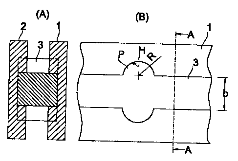
Fig. 1 is a drawing of a sectional structure of an NRD
guide according to an embodiment of the present invention.
In the drawing, numerals 1 and 2 denote conductive plates,
in which slots are formed on respective surfaces opposing
each other while a dielectric strip 3 is disposed between
both the slots. When designed in a frequency band of 60 GHz,
the size of each part of the NRD guide is as follows: a =
2.2 mm; b = 1.8 mm; g = 0.5 mm.
Fig. 2 includes a sectional view of the NRD guide and a
plan view in a state that the upper conductive plate is
removed. Fig. 2A is a sectional view at the line A-A of Fig.
2H. At predetermined positions of the dielectric strip 3
are formed convex portions "P" protruding to both sides in
the lateral direction and having a radius of curvature "R".
On internal surfaces of the conductive plate 1, concave
portions "H" are formed associated with the convex portions.
The shape of the slot of the upper conductive plate 2 is the
CA 02315399 2000-06-15
- 10 -
same as that of the conductive plate 1.
The results of transmission characteristics (reflection
characteristics) of the NRD guide shown in Figs. 1 and 2,
obtained by a three dimensional finite-element-method
analysis are shown in Figs. 3 to 6, under conditions that a
specific dielectric constant of the dielectric strip 3 is
2.04 and when the radius of curvature "R" of the convex
portion of the dielectric strip is respectively changed to
be: 0.5 mm; 0.6 mm; 0.7 mm; and 0.8 mm. In this manner,
when the size of the convex portion of the dielectric strip
is small, the convex portion has little effect thereon, such
that it is understood that excellent reflection
characteristics can be obtained in a designed frequency band
of 60 GHz. It is also understood that the frequency band
capable of low-loss transmission with scarce reflection is
changed by the radius of curvature "R". That is, the larger
the radius of curvature "R" of the convex portion formed in
the dielectric strip, the smaller the frequency band with
the minimum reflection is inclined to become. However, even
when the radius of curvature "R" is increased to be 0.8 mm
just like this example, the NRD guide can be still used in a
frequency band of 60 GHz.
Then, the structure of an NRD guide according to a
second embodiment will be described with reference to Figs.
7 and 8.
CA 02315399 2000-06-15
- 11 -
While the first embodiment was described in the context
of the transmission line for a millimetric wave in which the
dielectric strip is disposed between the two conductive
plates, in the second embodiment, a substrate and the
dielectric strip as well are arranged between two conductive
plates to form a millimetric wave circuit. Fig. 7 is a
sectional view thereof. In the drawing, numeral 4 denotes a
dielectric substrate while numerals 31 and 32 represent
respective dielectric strips, wherein the dielectric
substrate 4 is arranged so as to be sandwiched between the
two conductive plates 1 and 2 via the dielectric strips 31
and 32. In this example, in order to arrange the dielectric
substrate 4 at the intermediate position, the upper and
lower dielectric strips 31 and 32 have the same shape.
The result of a three dimensional finite-element-method
analysis is shown in Fig. 8, under conditions that
dimensions shown in Fig. 7 are: a2 = 2.2 mm; b2 = 1.8 mm; g2
- 0.5 mm; and t = 0.1 mm, a specific dielectric constant of
the dielectric strips 31 and 32 is 2.04, a specific
dielectric constant of the dielectric substrate 4 is 3.5,
and the convex portions formed in the dielectric strips 31
and 32 have the same shape as that shown in Fig. 2 in which
a radius of curvature "R" is 0.55 mm. From this result, it
is understood that in the NRD guide in which the substrate
is disposed, the dielectric strips can also be fixed in a
CA 02315399 2000-06-15
- 12 -
predetermined frequency band without deteriorating
reflection characteristics.
Then, the structure of an NRD guide according to a
third embodiment will be described with reference to Figs. 9
and 10.
While in the first and second embodiments are formed
the convex portions protruding from the dielectric strip and
having a semi-circular shape, in the third embodiment,
corner portions of the convex portions in the dielectric
strip and the concave portions on internal surfaces of slots
of the conductive plates have a smoothly curved surface
shape. In Fig. 9, the convex portion "P" of the dielectric
strip 3 has a curvature (cylindrical surface) connecting two
arcs having radii of curvature "R1" and "R2". When the
dielectric strip 3 is cut from a PTFE plate with an end mill,
milling can be performed by approximately equalizing the
radius of curvature "R2" to the radius of the end mill or
making it larger than the radius of the end mill. By
equalizing the "R2" to the radius of the end mill, the
processing time can be reduced, resulting in reduced
processing cost. On the other hand, as for cutting of slots
of the conductive plates, milling with an end mill can be
easily performed by forming corner portions of the concave
portion "H" to have a partial cylindrical surface. This can
be achieved by equalizing the radius of curvature "R1" to
CA 02315399 2000-06-15
- 13 -
the radius of the end mill or making it larger than that.
The result of a three dimensional finite-element-method
analysis is shown in Fig. 10 under conditions that
dimensions shown in Fig. 9 are: a = 2.2 mm; b = 1.8 mm; and
g = 0.5 mm, a specific dielectric constant of the dielectric
strip 3 is 2.04, the radius of curvature "R1" is 0.8 mm, and
the "R2" is 1.0 mm. In this manner, when corner portions of
the convex and concave portions respectively formed in the
dielectric strip and the slots of the conductive plates have
a curved surface, the desired reflection characteristics can
also be obtained.
Then, the structures of NRD guides according to a
fourth and a fifth embodiment will be described with
reference to Figs. 11 to 14.
While in the first to third embodiments, the convex
portions in the dielectric strip and the concave portions on
internal surfaces of slots of the conductive plates have a
curved surface, convex portions "P" having a rectangular
planner shape may be formed and corresponding concave
portions "H" may be formed on internal surfaces of slots of
the conductive plates, as shown in Fig. 11. As shown in Fig.
13, convex portions "P" having a triangular planner shape
may be formed and corresponding concave portions "H" may be
formed on internal surfaces of slots of the conductive
plates.
CA 02315399 2000-06-15
- 14 -
The result of a three dimensional finite-element-method
analysis is shown in Fig. 12 under conditions that
dimensions shown in Figs. 11 and 13 are: a = 2.2 mm; b = 1.8
mm; and g = 0.5 mm, a specific dielectric constant of the
dielectric strip 3 is 2.04, and sizes of the convex portion
of the dielectric strip shown in Fig. 11 are: c = 0.6 mm;
and d = 0.8 mm. The result of a three dimensional finite-
element-method analysis is shown in Fig. 14 under conditions
that sizes of the convex portion of the dielectric strip
shown in Fig. 13 are: a = 2.0 mm; and f = 0.8 mm. In this
manner, in any of examples, excellent reflection
characteristics can be obtained in a predetermined frequency
band.
Fig. 15 is a drawing of a structure of an NRD guide
according to a sixth embodiment. In this embodiment, a
clearance between the convex portion "P" formed in the
dielectric strip and the concave portions "H" formed on
internal surfaces of slots of the conductive plates 1 and 2
is created in the lateral direction of the dielectric strip
3. Even the guide has such the structure, the dielectric
strip 3 can be fixed to the conductive plates 1 and 2.
Fig. 16 is a drawing of a structure of an NRD guide
according to a seventh embodiment. While in the first to
sixth embodiments, the convex portions protruding in the
lateral direction of the dielectric strip 3 are formed
CA 02315399 2000-06-15
- 15 -
therein, in the seventh embodiment, concave portions "H"
oppositely recessed in the lateral direction of the
dielectric strip 3 are formed therein and corresponding
convex portions "P" are formed on internal surfaces of slots
of the conductive plates 1 and 2. Even the guide has such
the structure, reflection characteristics can be effectively
maintained by determining a size (radius of curvature) of
the concave portion "H" of the dielectric strip 3 within the
predetermined range.
The result of a three dimensional finite-element-method
analysis is shown in Fig. 17 under conditions that
dimensions shown in Fig. 16 are: a = 2.2 mm; b = 1.8 mm; g =
0.5 mm; i = 3.0 mm; and j = 1.4 mm, and a specific
dielectric constant of the dielectric strip 3 is 2.04. In
this manner, excellent reflection characteristics can be
obtained in a predetermined frequency band.
Fig. 18 is a drawing of a structure of an NRD guide
according to an eighth embodiment. In this embodiment, the
concave portion of the dielectric strip shown in Fig. 16 has
a triangular planner shape. The result of a three
dimensional finite-element-method analysis is shown in Fig.
19 under conditions that dimensions shown in Fig. 18 are: a
- 2.2 mm; b = 1.8 mm; g = 0.5 mm; i = 3.0 mm; and j = 1.4 mm,
and a specific dielectric constant of the dielectric strip 3
is 2.04. In this case, excellent reflection characteristics
CA 02315399 2000-06-15
- 16 -
can be also obtained in a predetermined frequency band.
Figs. 20 and 21 are drawings of NRD guides according to
a ninth and tenth embodiments and respectively show plans
thereof when the upper conductive plate is removed. While
in the first to the eighth embodiment, the concave portion
or the convex portion is formed on the internal surface of
the slot of the conductive plate corresponding to the convex
portion or concave portion formed in the dielectric strip,
the both shapes are not necessarily the same or similar
figures, and they may be different from each other as shown
in Figs. 20 and 21. In the case shown in Fig. 20, the
convex portion "P" having a rectangular planner shape is
formed in the dielectric strip 3 while the concave portion
"H" having an approximately semicircular planner shape is
formed on the internal surface of the slot of the conductive
plate 1, so that part of the convex portion in the
dielectric strip 3 is mated with the concave portion in the
conductive plate. In the case shown in Fig. 21, the convex
portion "P" having a semicircular planner shape is formed in
the dielectric strip 3 while the concave portion "H" having
a rectangular sectional shape is formed on the internal
surface of the slot of the conductive plate. In this case,
the root portion of the convex portion "P" in the dielectric
strip 3 is mated with the concave portion "H" formed in the
slot of the conductive plate.
CA 02315399 2000-06-15
- 17 -
Then, the structure of an NRD guide according to an
eleventh embodiment will be described with reference to Figs.
22 to 24.
In this embodiment, the effect of the reflection in the
connecting portion between the dielectric strips is reduced.
Fig. 23 includes a perspective view of a part of the
dielectric strip and a side view thereof. As shown in the
drawing, the dielectric strip is divided into two portions
along the surface parallel to the propagating direction of
the electromagnetic wave, and the length of each gap between
respective end faces of dielectric strips 31a and 32a and
respective end faces of strips 31b and 32b is designed to
have a length of one-quarter of the guide wavelength or a
length which is an odd-number multiple thereof, so that
reflecting waves cancel each other out.
Fig. 22 is a perspective view showing the structure of
the fixing portion of the dielectric strips to the
conductive plates. In the predetermined portions of the
upper and lower dielectric strips 31b and 32b, convex
portions "P" protruding in the lateral direction are formed
and corresponding concave portions "H" are respectively
formed on internal surfaces of the slots of the upper and
lower conductive plates. Owing to this structure, the two
upper and lower dielectric strips are fixed to the
conductive plates in the predetermined position.
CA 02315399 2000-06-15
- 18 -
Fig. 24 includes drawings of states of positional
slippage when plural combinations of such the pair of
dielectric strips shown in Fig. 22 are connected together.
Fig. 24(A) shows the state that the length of each gap
between end faces of the strips 31a and 32a and end faces of
the strips 31b and 32b are to have zero at the standard
temperature. When each dielectric strip is not fixed, each
of gaps between dielectric strips at connecting end faces is
not the same, as shown in Fig. 24(B), and difference in the
degree of reflection is produced, so that the above-
mentioned cancellation of reflected waves by superimposing
them out of phase with each other does not always
effectively act thereon. Then, as shown in Fig. 24(C), when
each dielectric strip is fixed to the conductive plate at
approximately intermediate position of the dielectric strip,
each gap length "DL" between dielectric strips at connecting
end faces is the same even when temperature changes, so that
the cancellation of reflected waves by superimposing them
out of phase effectively acts thereon. In addition, Fig. 22
shows the fixing structure of the dielectric strip to the
conductive plate in a fixing reference line shown in the
drawing, for example.
Then, a structure of an integrated circuit for a
millimetric wave radar will be described with reference to
Fig. 23.
CA 02315399 2000-06-15
- 19 -
Fig. 25 is a plan view thereof in a state that the
upper conductive plate is removed. This integrated circuit
for a millimetric wave radar comprises various components
such as an oscillator unit, an isolator unit, a coupler unit,
a circulator unit, a mixer unit, and a primary radiator unit
and a dielectric lens of an antenna. In the oscillator unit,
numeral 51 denotes a Gunn diode block and one electrode of a
Gunn diode is connected to a line formed on a substrate. In
the oscillator unit, a dielectric strip 53 and a dielectric
strip 54 form a sub-line and a main line, respectively.
Numeral 52 denotes a dielectric resonator connected with
both the lines. Although eliminated in the drawing, a
varactor diode is connected to the dielectric strip 53 as
the assistant line such that the oscillating frequency of
the Gunn diode is controllable. In the isolator unit,
dielectric strips 55, 56, and 57 and a terminating set 59
are disposed. In the central portion of the three
dielectric strips 55, 56, and 57, a ferite resonator 70 is
disposed to form a circulator. The circulator and the
terminating set 59 form an isolator. In the coupler unit,
dielectric strips 60 and 61 form a coupler. In the
circulator unit, dielectric strips 62, 63, and 66 and a
ferite resonator 71 form a circulator. In the primary
radiator unit, a dielectric strip 64 and a dielectric
resonator 65 as a primary radiator are disposed.
CA 02315399 2000-06-15
- 20 -
Furthermore, in the mixer unit, dielectric strips 67, 68,
and 72 are disposed and a conductive pattern generating an
IF signal (intermediate-frequency signal) by mixing an RF
signal (receiving-frequency signal) and an Lo signal (local
signal) together and a mixer diode are arranged on the
substrate. The oscillating signal generated by the Gunn
diode block 51 is transmitted through the path of the
dielectric strip 54 -~ the isolator unit -~ the dielectric
strip 60 -~ the circulator unit -~ the primary radiator unit
so as to be radiated via the dielectric lens. The
receiving-frequency signal is transmitted through the path
of the dielectric lens --> the primary radiator unit --~ the
circulator unit ~ the mixer unit, while the Lo signal is
transmitted through the path of the coupler unit ~ the
mixer unit.
As shown in Fig. 25, in each dielectric strip and each
terminating set, mating portions (convex portions) mating
with internal surfaces of the slots of the conductive plates
are formed at predetermined positions while corresponding
concave portions are formed on internal surfaces of the
slots of the upper and lower conductive plates. Therefore,
these dielectric strips and terminating sets are positioned
and fixed in the propagating direction of the
electromagnetic wave. When the dielectric strip and the
terminating set expand and contract in accordance with
CA 02315399 2000-06-15
- 21 -
variations in ambient temperature, the gap between the
dielectric strips at the connecting portion between
components is produced to be determined directly and
exclusively. Accordingly, variations in characteristics due
to variations in assembly accuracy and variations in
temperature are easily kept within a predetermined range.
In addition, the mating position in each dielectric
strip may be designed in consideration of productivity of
the dielectric strip and variations in characteristics due
to changes in temperature. Whether convex or concave
portions formed in the lateral direction of the dielectric
strip may also depend on productivity and variations in
characteristics. For example, when convex portions
protruding in the lateral direction are formed in a bend
portion, the portion becomes a propagating area in the LSE01
mode. In order to prevent a loss involved in the mode
conversion from the LSMO1 mode to the LSE01 mode, concave
portions recessed in the lateral direction of the dielectric
strip may be formed therein, as shown by "A" in Fig. 25.
When the mating portion is formed at positions except the
bend portion, the convex portions protruding in the lateral
direction of the dielectric strip may be formed therein such
that processing of the slot of the conductive plate is easy
and the strength of the dielectric strip can be maintained.
According to the invention described in Claim 1, since
CA 02315399 2000-06-15
- 22 -
the dielectric strip is fixed in the propagating direction
of the electromagnetic wave by mating of the convex portions
or the concave portions of the dielectric strip with
internal surfaces of the slots of the conductive plates,
even when the dielectric strip and the slots of the
conductive plates are produced by machining, etc., the
process is easily performed. Since the convex portions or
the concave portions of the dielectric strip 3 are formed in
the lateral direction thereof, the electromagnetic field
distribution in a mode to be propagated can be scarcely
disturbed.
According to the invention described in Claim 2, for
example, when the dielectric strip is cut from a dielectric
plate with an end mill, the dielectric strip having the
concave portions or the convex portions with corner portions
having a curved surface shape can be easily processed
corresponding to the radius of the end mill. Likewise, when
the slot of the conductive plate is formed with the end mill,
the concave portion or convex portion with corner portions
having a curved surface shape can be easily formed on the
internal surface of the slot of the conductive plate
corresponding to the radius of the end mill.
According to the invention described in Claim 3, in the
connecting portion of non-radiative dielectric lines,
reflected waves in each connecting surface between the
CA 02315399 2000-06-15
- 23 -
dielectric strips cancel each other by being superimposed
out of phase with each other, such that the effect of the
reflection is reduced. Even when the two divided dielectric
strips move relative to the conductive plates due to
variations in temperature, since the length of each gap
produced therein is the same, the effect of the reflection
is reduced regardless of variations in ambient temperature.
According to the invention described in Claim 4, since
the positional relationship between plural non-radiative
dielectric lines can be maintained to be stable, an integral
circuit having small variations in characteristics due to
variations in assembly accuracy and to variations in ambient
temperature after assembling can be obtained.
Industrial Applicability
As understood by the above description, a non-radiative
dielectric line and an integrated circuit thereof according
to the present invention are applied to the production of
wide-ranging electronic apparatuses such as millimetric-wave
frequency-band radio communication apparatus and a
microwave-frequency-band radio communication apparatus.