Note : Les descriptions sont présentées dans la langue officielle dans laquelle elles ont été soumises.
CA 02317751 2000-07-07
WO 99/35762 PCT/US99/00140
1
METHOD AND APPARATUS FOR INCREASING SPECTRAL
EFFICIENCY OF CDMA SYSTEMS USING DIRECT SEQUENCE
SPREAD SPECTRUM SIGNALS
BACKGROUND OF INVENTION
1. Field of the Invention
The present invention relates to broadband communication systems and
particularly to systems for transmission and reception of pseudorandom noise
sequences
and spread spectrum signals, and to code division multiple access systems with
application to satellite and terrestrial communications.
2. Description of the Related Art
Spread spectrum systems have been used for many years in digital
communications. A spread spectrum signal consists of a baseband message signal
modulated onto a Garner and thereafter spread in frequency by a pseudorandom
noise
sequence ("PN sequence" or "PNS'~, independent of the message signal itself.
The
receiver then recovers the message signal by using a replica of the PN
sequence. The
main advantages of spread spectrum systems are good interference and noise
rejection,
low power density, ability to access multiple channels (such as in code
division multiple
access (CDMA) systems), high resolution ranging, and message protection. The
ratio of
the bandwidth of the PNS to that of the message signal, called the processing
gain,
determines the merit of the system.
Typical block diagrams of a spread spectrum transmitter and receiver are found
in J. K. Holines, coherent Spread SRectrum S s~r~tems (Wiley 1982), and
reproduced as
Figures 1 a and lb. In the transmitter in Figure 1 a, a digital message signal
transmitted
at bit rate B is provided to coder 104. This coder encodes the data bits into
codewords
for transmission and can be a block coder or a convolutional coder as
described in G. C.
Clark and J. B. Cain, Error-Correction CodinE for D'gital Com_rnLn_ications
(Plenum
Press 1981). PNS modulator 106 modulates (or spreads) the coded signal with a
PN
CA 02317751 2000-07-07
WO 99/35762 PCT/US99/00140
2
sequence from PNS generator 110. Carrier frequency generator 112 generates a
carrier
signal that is modulated by the spread coded signal in carrier modulator 108.
The PN
sequence is a digital signal made up of "chips" and whose chip interval or
chip period is
much smaller than the data bit period (thus the bandwidth of the PN sequence
is much
S greater than that of the data signal). The resulting signal is amplified by
amplifier 120
and transmitted by antenna 130.
As depicted in Figure lb, the transmitted signal is received by antenna 150
and
amplified by amplifier 160. The received signal is provided to carrier
restoration and
phasing module 166 which provides a local oscillator signal which is phase
synchronized
to the carrier signal. The local oscillator signal is used to demodulate the
carrier from the
received signal in coherent detector 162. The resulting demodulated signal is
provided
to tracking and acquisition (T&A) synchronism device 168 to establish
synchronization
between the demodulated signal and a local PNS generator in T&A synchronism
device
168 which generates a replica of the PNS that was used in the transmitter. In
the
acquisition stage, a coarse alignment between the replicated PNS and the
demodulated
signal is performed using serial and/or sequential search, sequential
estimation, universal
timing, or matched filter algorithms. These techniques are described in
various
references, one of which is R. C. Dixon, ~~read Syectrum Systems with
Commercial
Annlications (Wiley 1994). The acquisition stage brings the replicated PNS and
the
demodulated signal within ,half a chip interval of each other. Once the
demodulated
signal is acquired, the two signals are tracked, generally using a delay-lock
loop. $g~,
gig" J. J. Spilker, Djgital Communications by Satellite (Prentice Hall 1977).
Once
synchronized, T&A synchronism device 168 outputs the synchronized replicated
PNS
to PNS demodulator 164 which fiuther demodulates (despreads) the modulated
signal to
produce a baseband coded data signal which is provided to decoder 170. Decoder
170
contains circuitry to extract the clock signal, to determine whether code bits
are high or
low, to synchronize the code frames, and to convert coded bits into message
data bits.
A two-channel version of this spread spectrum system is described in United
States Patent No. 5,414,728 to Zehavi, and depicted in Figures 2a-2c. In the
transmitter
of Figure 2a, two message signals, User A and User B, are transmitted at bit
rate B in I
(in-phase) and Q (quadrature phase) channels, respectively, or a single user
at bit rate 2B
CA 02317751 2000-07-07
WO 99/35762 PC"T/US99/00140
3
is demultipiexed in demultiplexor 202 and transmitted in the I and Q channels.
The two
signals are then respectively supplied to I and Q channel coders 204a and
204b. Each
channel is spread by a separate PN sequence, the I-channel by PNS, generated
by PNSI
generator 210a, and the Q-channel by PNSQ generated by PNSQ generator 21 Ob.
In PNS
modulators 206a and 206b, the coded signals modulate the respective PNS, the
result
being provided to I-channel carrier modulator 208a and Q-channel carrier
modulator
208b, respectively. An in-phase carrier signal produced by carrier frequency
generator
212 is modulated (usually by binary phase shift keying or BPSK) in I-channel
carrier
modulator 208a by the spread coded signal to produce an I-channel signal that
is
provided to summing amplifier 220. The in-phase carrier signal is phase
shifted by 90°
in phase shifter 214 and then BPSK-modulated in Q-channel carrier modulator
208b by
the spread coded signal to produce a Q-channel signal which is added to the I-
channel
signal in summing amplifier 220 and provided to antenna 230 for transmission.
The receiver of Figure 2b processes the two channels, receiving the
transmitted
signal in antenna 250 and amplifying it in amplifier 260. As before with the
single
channel system depicted in Figure lb, the carrier signal is restored in
carrier frequency
restoration and phasing module 266. Carrier restoration module 266 provides in-
phase
and quadrature-phase carrier signals which are used to demodulate the received
signal in
coherent detector 262 into received i and Q component signals. Each of these
is used in
T&A synchronism device 268 to acquire and track the received signals and to
produce
a timing signal which is provided to PNS, generator 265a, and PNSQ generator
265b.
PNSI generator 265a replicates PNS, to despread the received I-channel signal,
and PNSQ
generator 265b replicates PNSQ to despread the received Q-channel signal. In
PNS
demodulator 264, shown in more detail in Figure 2c, each channel is split into
subchannels. One subchannel from each channel is then multiplied with PNS~ in
multipliers 284a and 284b, and the other subchannel is multiplied with PNSQ in
multipliers 282a and 282b. The four products are accumulated in accumulators
286a,
286b, 288a, and 288b for one PNS period (illustrated by switches 290ay 290b,
292a, and
292b and delay elements 294a, 294b, 296a, and 296b). The accumulated results
finm the
subchannels in the I and Q channels that were multiplied by PNS, are provided
to phase
rotator 298a, and the integrated results of the subchannels in the I and Q
channels that
CA 02317751 2000-07-07
WO 99/35762 PCT/US99/00140
4
were multiplied by PNSQ are provided to phase rotator 298b. These phase
rotators
estimate the data sequences that were transmitted in each channel.
This prior art system is limited in its spectral efficiency, thus limiting the
number
of users or the data rate of the system or both. Spectral effciency is defined
by
2B N
S y = ~ , where Bm is the data rate of the information signal that modulates
the PN
sequences, dF is the occupying frequency range, and N is the number of
subscriber
stations (information streams) working within the same fiequency range at the
same time.
In orthogonal CDMA (OCDMA), it is necessary to allocate for each subscriber
station
two PN sequences, each sequence being of signal base (length) D. Thus, N = D ,
where
D = BF ; therefore N = ZB . In this prior art system, Bm = B, the data rate of
the
nr m
information signal provided to PNS modulators 206a and 206b in Figure 2a.
Substituting
into the spectral efficiency equation, y = ( ~) ~ ( B ) and y = 1 bitlsec/Hz.
It is an
object of the present invention to double the spectral efficiency of a spread
spectrum
system by decreasing the bit rate of the information signal provided to the
PNS
1 S modulator and by using two PN sequences on both the I and Q channels.
SUMMARY OF THE INVENTION
The improved spread spectrum system includes a modulator and demodulator for
use in a spread spectrum system operating at nominal data rate B. The
modulator, which
can be a spreader or an encoder, processes I and Q channels and includes a PN
sequence
generator that generates two orthogonal PN sequences. Each channel includes a
demultiplexor, a switch, and a modulo-2 adder. In each channel, the data
signal is
demultiplexed into two data signals operating at half the nominal data rate.
One
demultiplexed signal is sent to the trigger of the switch, determining which
of the two PN
sequences the switch outputs, depending on whether the demultiplexed signal is
high or
low. The other demultiplexed signal is modulo-2 added (exclusive-OR'd) to the
PNS
CA 02317751 2000-07-07
w0 99/35762 PCT/US99/00140
provided by the switch, and the modulo-2 sum is transmitted as the channel
output. The
modulator can process two data channels at bit rate B or one high speed
channel at bit
rate 2B that is demultiplexed into two nominal rate data channels.
The demodulator, which can be a despreader or a decoder, processes I and Q
5 channels and includes a PN sequence generator that generates replicas of the
PN
sequences that were used in the modulator. Each channel is divided into two
subchannels, each subchannel including a multiplier, an integrator, and a
decision circuit.
Each channel also includes a channel decision circuit, a switch, and a
multiplexor. The
received data signal is split into the two subchannels, one branch being
multiplied by the
first PNS and the other branch multiplied by the second PNS. The multiplier
outputs are
integrated and provided to the subchannel decision circuit to determine
whether the bit
is high or low. The absolute values of the integrated results are also
compared in the
channel decision circuit which provides a trigger signal and a control signal.
The control
signal is high or low depending on which subchannel had the higher integrated
result (i.e.
control signal is high if the subchannel multiplied by the first PNS had a
greater
integrated result; control signal is low otherwise). The trigger signal
triggers the switch
to pass the data bit from the subchannel whose integrated result was greater.
The switch
output and the control signal, both operating at half the nominal data rate,
are multiplexed
and the combined output is the channel output at the nominal data rate. If
there is a
single, high-speed user, the two channel outputs are multiplexed to provide a
single
output at twice the nominal data rate.
This invention doubles the spectral efficiency as compared with that of the
prior
art. As before, N = D where D = B . However, the bit rate BM in the
denominator
m
of this equation is the bit rate of the data that modulates the PN sequences,
i.e. 2 in the
present invention. Thus, D = ~ _ Z ~ , N = 2 ~ - ~ , and y = ~_2B ) , ~ OF )
B B 2B B OF' B
2
and y = 2 bit/seclHz. The increase in y means that the system capacity is
higher within
the specific frequency band. This higher capacity can be realized with higher
data rates,
more users, or a combination according to the equation BT = BU ~ U, where BT
is the
CA 02317751 2000-07-07
WO 99/35762 PCT/US99/00140
6
capacity of the whole system, Bu is the data rate of one user, and U is the
number of
users. With a two-fold increase in system capacity, while keeping B~ constant,
U could
double, or BU could double keeping U constant, or both could increase less
than two-fold.
BRIEF DESCRIPTION OF THE DRAWINGS
Figure 1 a is a block diagram of a prior art spread spectrum transmitter;
Figure lb is a block diagram of a prior art spread spectrum receiver;
Figure 2a is a block diagram of a second prior art spread spectrum
transmitter;
Figure 2b is a block diagram of a second prior art spread spectrum receiver;
Figure 2c is a detailed block diagram of the PNS demodulator in Figure 2b;
Figure 3a is a block diagram of the transmitter of the improved spread
spectrum
system;
Figure 3b is a block diagram of the modulator within the transmitter of Figure
3a;
Figure 3c is a block diagram of the switch within the spreader of Figure 3b;
Figure 4 is a timing diagram of the bits within the modulator;
Figure Sa is a block diagram of the receiver of the improved spread spectrum
system.
Figure Sb is a block diagram of the demodulator within the receiver of Figure
Sa;
and
Figure 6 is a timing diagram of the bits within the demodulator.
DETAILED DESCRIPTION OF THE INVENTION
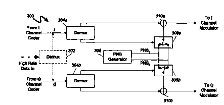
Figure 3a is a block diagram of the improved transmitter in accordance with
the
present invention. In place of PNS~ and PNSQ generators 210a and 210b and PNS
modulators 206a and 206b is modulator 300, which can more specifically be used
as an
encoder or a spreader. Thus, although pictured in Figure 3a between channel
coders 204a
and 204b and channel carrier modulators 208a and 208b, modulator 300 could be
used
as an encoder and thus be used in place of channel coders 204a and 204b. In
addition,
modulator 300 could be placed after channel carrier modulators 208a and 208b
as a
spreader because the spreading function can be performed either before carrier
CA 02317751 2000-07-07
WO 99/35762 PC1'NS99/00140
7
modulation or after it. As shown in Figure 3a, it is preferable to use
modulator 300 as
a spreader and locate it after channel coders 204a and 204b.
Figure 3b is a block diagram of the modulator within the transmitter of Figure
3a.
Modulator 300 operates on both the I and Q channels. Each channel includes a
demultiplexor 304, a switch 308, and a modulo-2 adder 310 (also called an
exclusive-OR
gate). Modulator 300 also includes PNS generator 306 that generates two
orthogonal PN
sequences.
Digital data, at bit rate B, is provided on both I and Q channels from channel
coders 204a and 204b, each channel representing a user. The typical number of
users
provided for in this system is an even number (i.e. divisible by 2). The
maximum
number of users depends on the frequency bandwidth dF. However, there could be
an
odd number of users if a higher bit rate is chosen keeping dF constant. In
Figure 3b, this
is represented as one channel operating at rate 2B provided to modulator 300.
In such a
case, the data is separated using demultiplexor 302 into two data streams each
operating
at B. It can be seen that in such a case, demultiplexor 302 takes the place of
demultiplexor 202 in Figure 3a and channel coders 204a and 204b would be
replaced by
one high speed channel coder (not shown) placed before demultiplexor 302.
The choice of data rate B is not critical, although it must conform to the
main
requirement of spread spectrum systems in which the bandwidth of the system
must be
much higher than that of the data rate, i.e. dF » B. Typical data rates can be
32, 64, 80,
160, 320, 640, or 1280 kb/s, none of which is more preferable than another.
The two PN sequences can be generated by any known method, the most common
of which uses a shift register. See~e.~., S. W. Golomb, Shift Register
Se~~uences
(Aegean Park Press 1982) or R. C. Dixon, S rep ad Spectrum Systems with
Commercial
,Apa~lications (Wiley 1994). Each PN sequence can be any length divisible by
four in
order to preserve orthogonality. The length M of a PNS period is related to
the
bandwidth dF and bit rate B by dF = B ~M . In order to preserve processing
gain, dF »
B, M should be at least 32 and possibly 64. On the high side, selection of M
is limited
by the acquisition time in the receiver, so it is preferable not to select M
too large. The
chip rate is generally equal to dF and is thus approximately B ~M: The chip
rate can be
CA 02317751 2000-07-07
WO 99/35762 PCT/US99/00140
8
very high (> 1 GHz), however it is preferable to use one that is a power of
two because
it is easier to produce those rates (i.e. 512, 1024, 2048, 4096, 8192 kHz).
Modulator 300 operates as follows, considering the I-channel as exemplary (the
Q-channel operates the same way). Data is provided at bit rate B to
demultiplexor 304a
in which it is separated into two data signals operating at rate 2 . One data
signal is
provided to the trigger of switch 308a and the other signal is provided to
modulo-2 adder
310a. The two PN sequences, PNS, and PNSZ are provided as inputs to switch
308x.
Switch 308a is further described in Figure 3c. The switch includes trigger
312, two AND
gates 314 and 316, and OR gate 318. Trigger 312 operates like a flip-flop in
which one
of the trigger's outputs follows the input and the other output provides the
inverse of the
input. Thus, if the trigger signal from demultiplexor 304 is 1, the top output
from trigger
312 will be 1 and PNS, will be transmitted to the switch .output. Conversely,
if the
trigger signal is 0, the bottom output from trigger 312 will be 1 allowing
PNSZ to be
transmitted to the switch output. Because adder 310a adds by modulo-2, if the
input
from the demultiplexor to adder 310a is a 0, the adder will output the PNS,
and if the
demultiplexor output is a 1, the adder will output the inverse of the PNS. The
chip rate
of the modulated output from modulator 300 is ~ ~ M.
Figure 4 is a timing diagram of the bits at different places within modulator
300.
Figure 4(a) shows the data signal at the input to demultiplexor 304a operating
at bit rate
B. Figure 4(b) shows the odd bits output from demultiplexor 304a at bit rate 2
and
provided to modulo-2 adder 310a. Figure 4(c) shows the even bits output from
demultiplexor 304a at bit rate 2 and provided to switch 308a as the trigger
signal.
Figures 4(d) and 4(e) show PNS, and PNSZ, respectively, provided by PNS
generator
306. For ease of illustration, consider PN sequence periods of length 8 bits,
i.e. M = 8.
PNS, is a 7-bit Barker sequence with an added 0, i.e. 11100100, and PNSZ is
the 7-bit
Barker sequence used in PNS, shifted four bits with an added 0, i.e. 00101110.
Both PN
sequences operate at rate i ~ M = ~ ~ 8 = 4B . Figure 4(f) shows the output
from
switch 308a given the trigger signal of Figure 4(c). The switch output
operates at bit rate
4B. When the trigger signal is 1, switch 308a outputs PNS,; when the trigger
signal is
0, switch 308a outputs PNS2. Figure 4(g) shows the channel output at bit rate
4B. When
the signal in Figure 4(b) is a 1, modulo-2 adder 310a outputs the inverse of
the PN
CA 02317751 2000-07-07
WO 99/35762 PCTNS99/OOi40
9
sequence at its input; when the signal in Figure 4(b) is a 0, modulo-2 adder
310a outputs
the PN sequence at its input.
Figure 5a is a block diagram of the improved receiver in accordance with the
present invention. In place of PNS, and PNSQ generators 265a and 265b and PNS
demodulator 264 is demodulator 500, which can more specifically be used as a
despreader or a decoder. Thus, although pictured in Figure 5a between coherent
detector
262 and decoder 270, demodulator 500 could be used as a decoder and thus
partially be
used in place of decoder 270. (As a decoder, demodulator 500 could not fully
replace
decoder 270 because the latter includes clock extraction circuitry and frame
synchronization circuitry that demodulator 500 does not include.) In addition,
demodulator 500 (along with T&A synchmnism device 268) can be placed before
coherent detector 262 (and Garner restoration and phasing module 266) and used
as a '
despreader because the despreading function can be performed either before
coherent
detection or after it. As shown in Figure 5a, it is preferable to use
demodulator 500 as
a despreader and locate it after coherent detector 262.
Figure 5b is a block diagram of the demodulator within the receiver of Figure
5a.
It is assumed that T&A synchronism device 268 synchronizes in a conventional
manner
PNS generator 520 and controls the decision circuits and multiplexors in
demodulator
500. Demodulator 500 operates on both the I and Q channels, each channel being
split
into subchannels. Each channel includes multipliers 502 and 504, integrators
506 and
508, channel decision circuit 510, subchannel decision circuits 512 and 514,
switch 516,
and multiplexor 518. Demodulator 500 also includes PNS generator 520 that
generates
replicas of the two orthogonal PN sequences used in modulator 300.
Digital data, at bit rate 2 ~ M, is provided on both I and Q channels from
coherent detector 262. Using channel I as exemplary, the data in I channel is
split into
upper and lower subchannels. In the upper subchannel, the data is multiplied
in
multiplier 504a by PNS,, and the pmduct is provided to integrator 506x.
Similarly, in the
lower subchannel, the data is multiplied by PNSZ in multiplier 502x, and the
product is
provided to integrator 508a. Integrators 506a and 508a integrate over one PNS
period
(Mbits). Subchannel decision circuits 512a and 514a determine whether the
integrated
output is a 0 or a 1 and provide those bits to switch 516a. Channel decision
circuit 5 l0a
CA 02317751 2000-07-07
~O 99/35762 PC'T/US99/00140
decides which subchannel has the largest integrated output magnitude (absolute
value).
This decision determines that the PNS contributing to the larger integrated
value was the
one that was used in modulator 300. Channel decision circuit S l0a has two
outputs. One
output provides a control signal corresponding to the PNS that contributed to
the larger
5 integrated value. The other output provides a signal to the trigger of
switch S 16a to
output the bit from the subchannel decision circuit corresponding to larger
integrated
value. For example, if the value from integrator SO8a is greater than the
value from
integrator 506a, channel decision circuit S l 0a determines that PNSZ
modulated that bit,
and channel decision circuit S l0a provides a 0 to one input of multiplexor
518a. The
10 trigger output from channel decision circuit S l0a directs switch 516a to
output the bit
from subchannel decision circuit 514a and provide it to the second input of
multiplexor
S 18a. The inputs to multiplexor 518a operate at bit rate ~ . IVIultiplexor
518a combines
the two inputs into one data signal operating at bit rate B.
The Q channel works analogously, and multiplexor 518b provides a data signal
also operating at bit rate B. If two user data signals at bit rate B had been
transmitted in
Figure 3a, the two outputs firom demodulator 500 are provided to decoder 270
for further
demodulation. If only one high speed data signal at bit rate 2B had been
transmitted in
Figure 3a, two scenarios exist for combining the two outputs of demodulator
500. In the
first scenario, the outputs of multiplexors S 18a and S 18b can be further
combined in
multiplexor 522 to form one data signal at bit rate 2B, and decoder 270 would
only
operate on that data signal. In that case, multiplexor 280 in Figure Sa is no
longer
needed. In the second scenario, demodulator 500 can still provide two data
signals to
decoder 270 and the outputs from that module can be combined in multiplexor
280
instead.
Figure 6 is a timing diagram of the bits at different places within
demodulator
500. Figure 6(a) shows the data signal at the input to multipliers 502 and 504
operating
at bit rate 2 ~ M = 2 ~ 8 = 4B . (This is the same waveform as in Figure
4(g).)
Figures 6(b) and 6(c) show PNS, and PNS2, respectively, provided by PNS
generator
520. These are the same waveforms as in Figures 4(d) and 4(e), respectively.
Figures
6(d) and 6(e) show the outputs from integrators 506a and 508a, respectively.
These
values were derived from multiplying bit-by-bit the waveform in Figure 6(a)
with the
CA 02317751 2000-07-07
WO 99/35762 PCTNS99/00140
11
appropriate PNS. When the bits were different, the multiplier produced +1;
when the bits
were the same, the multiplier produced -1. The integrators added up all eight
bits. For
the first data bit, the subchannel corresponding to PNS, produced the greater
integrated
output. Thus, the waveform in Figure 6(f), showing the control signal from
channel
S decision circuit S 10a, records a 1 corresponding to PNS,. Likewise, when
the subchannel
corresponding to PNSZ produces the larger integrated result, the waveform in
Figure 6(f)
records a 0. The waveform in Figure 6(f) operates at 2 . Note that the
comparison in
channel decision circuit S l0a is based on the absolute value of the
integrated outputs.
The sign of the integrated outputs comes into play in Figure 6(g). This
waveform
corresponds to the value of the bit produced by the decision circuit of the
subchannel
corresponding to the larger integrated value. If the sign is positive, the bit
produced is
a 1; if the sign is negative, the bit produced is a 0. The waveform in Figure
6(g) also
operates at 2 . Finally, the two waveforms in Figures 6(f) and 6(g) are
combined in
multiplexor 518, Figure 6(f) constituting the even bits and Figure 6(g)
constituting the
odd bits in the multiplexed output. The resulting signal in Figure 6(h)
operates at bit rate
B and is the same signal as the input waveform in Figure 4(a).
An advantage of the present invention is that it is well adapted for group
users and
ISDN services. As an example, assume there are four subscribers and that each
subscriber operates at a data rate of B + D = 64 + 16 = 80 kb/sec. These four
subscribers
are connected directly to switches 308a and 308b and to modulo-2 adders 310a
and 310b
in Figure 3b (i.e. directly to the output of demultiplexors 304a and 304b),
and are
synchronized with each other. The total transmission daxa rate equals 4 ~ 80 =
320 kb/sec,
and the signal base D equals 64. Thus, dF = D ~ B = 64 ~ 80 kb/sec = 5120 kHz
~ 5 MHz.
A group signal having the same data rate (320 kb/sec) can be provided at the
input to
demultiplexor 302. The group signal for that number of subscribers remains
constant,
simplifying construction of a transmitting radio highway. If the number of
subscribers
is reduced, the block diagram will remain unchanged and only the inputs of the
non-
operating subscribers will be cut off The peak factor of the radio signal will
still equal
1. At the receiver in Figure Sb, each subscriber, from switches 516a and 516b
and
decision circuits S l0a and S l Ob (the inputs to multiplexors S 18a and
518b), outputs at
a rate of 80 kb/sec, and the group output from multiplexor 522 operates at 320
kb/sec.
CA 02317751 2000-07-07
WO 99/35762 PC'T/US99/00140
12
By using OCDMA, N = ~ - 24 = 3 2 subscriber stations of this kind cup be
arranged.
Thus the spectral efficiency is y = 32 ~ 320 kb/sec = 2 bitlseclHz .
5120 kHz
In the case where the number of subscribers in a group is higher than four,
for
example, eight or nine, it may be practical to allocate a common signaling
channel
operating at 64 kb/sec. This produces a group data rate of 9 ~ 64 + 1 ~ 64 =
640 kb/sec
which can be provided to demultiplexor 302 in Figure 3b. Using the same signal
base
D = 64, the chip frequency equals 160 kb/sec ~ 64 =10240 kb/sec. In this case,
only the
operating data rates of the elements are doubled, but this does not change
either the block
diagrams of the modulator and demodulator or the principle of operation.
While several embodiments have been illustrated and described, other
variations
and alternate embodiments will occur to those skilled in the art. These
variations and
embodiments remain within the spirit and scope of this invention.