Note : Les descriptions sont présentées dans la langue officielle dans laquelle elles ont été soumises.
CA 02318146 2003-02-26
GAIN CONTROL AMPLIFIER, VARIABLE GAIN AND AUTOMATIC
GAIN CONTROL AMPLIFIERS INCLUDING DIFFERENTIAL
CIRCUIT TRANSISTORS AND CURRENT SPLITTER
Technical Field
The present invention relates to a gain control amplifier, a variable gain
amplifier and an automatic gain control amplifier using the variable gain
amplifier.
Background Information
Automatic gain control (AGC) amplifiers are commonly used in receivers.
The overall performance of receivers depend on the input dynamic ranges and
noise factors of the AGC amplifiers. The input dynamic range is defined by the
ratio of the maximum input signal amplitude for linear operation of the AGC
15 amplifier and the minimum input signal for which the output amplitude is
the
nominal output amplitude of the amplifier. The output dynamic range is defined
as the ratio of the maximum output signal and the minimum output signal for a
given input dynamic range. For most of the applications, the input dynamic
range is 100 to 300 (40 to 50 dB) and the output dynamic range is 1.2 to 1.5
(1.5 to
20 3.5 dB). The noise factor is a measure of the amplifier equivalent input
noise and
is defined as the degradation of the signal to noise ratio due to the AGC
noise. In
general, the input dynamic range for linear operations must be large to
accommodate without degradation different applications and the equivalent
input noise must be low to minimize the signal to nose ratio degradation.
Summary Of The Invention
It is an object of the present invention to provide improved gain control
amplifier, variable gain amplifier and AGC amplifier.
According to one aspect of the present invention, there is provided a gain
30 control amplifier for amplifying an input voltage and providing an
amplified
output voltage, comprising first, second and third differential circuits and
current
split means.
The first differential circuit comprises first and second transistors, the
emitters of which are coupled, and a first load element connected to the
collector
of the first transistor.
The second differential circuit comprises third and fourth transistors, the
emitters of which are coupled, and a second load element connected to the
CA 02318146 2000-07-13
WO 00/41298 PCT/CA99/01203
2
collector of the fourth transistor, the bases of the third and fourth
transistors
being coupled to the bases of the second and first transistors, respectively,
the
amplified output voltage being provided from the collectors of the first and
fourth transistors.
The third differential circuit comprises fifth and sixth transistors, the
emitters of which are coupled through a pair of resistance elements, the
junction
of the resistance elements being connected to a first current circuit, the
collector
of the fifth transistor being connected to the coupled emitters of the first
and
second transistors, the collector of the sixth transistor being connected to
the
coupled emitters of the third and fourth transistors, the input voltage being
fed
to the bases of the fifth and sixth transistors.
In the gain control amplifier, the current split means splits current
flowing iu 1W first anc~ ~P~~nd load elements from the respective transistors.
The current flowing in the fifth transistor of the third differential circuit
is
proportional to the difference between the current flowing in the first load
element and the split current. Similarly, the current flowing in the sixth
transistor of the third differential circuit is proportional to the difference
between the current flowing in the second load element and the split current.
Due to current splitting, relatively small currents drive the fifth and sixth
transistors which amplify the input voltage. Since the relatively small
currents
flow in the resistance elements coupled to the emitters of the fifth and sixth
transistors, noise caused by the transistors is relatively low. Thus, it
provides a
wide input dynamic range with low noise.
For example, the current split means comprises fourth and fifth
differential circuits. The fourth differential circuit comprises seventh and
eighth
transistors, the emitters of which are coupled, the coupled emitters being
connected to a second current circuit, the collector of the seventh transistor
being connected to the collector of the first transistor, the bases of the
seventh
and eight transistors being connected to the bases of the second and first
transistors, respectively. The fifth differential circuit comprises ninth and
tenth
transistors, the emitters of which are coupled, the coupled emitters being
connected to a third current circuit, the collector of the tenth transistor
being
connected to the collector of the fourth transistor, the bases of the ninth
and
tenth transistors being connected to the bases of the fourth and third
transistors,
respectively. The current split means further comprises split control means
for
controlling currents flowing in the transistors of the differential circuits
in
response to a voltage difference between the voltages at the collectors of the
first
SUBSTITUTE SHEET (R ULE 16)
CA 02318146 2000-07-13
WO 00/41298 PCT/CA99/01203
3
and fourth transistors. The split control means comprises base voltage control
means for generating a variable base voltage in response to the voltage
difference, the variable base voltage being fed to the bases of the
transistors of
the first, second, fourth and fifth differential circuits. In response to the
variable
base voltage, the currents flowing in the transistors of the first, second,
fourth
and fifth differential circuits are varied to vary the amplifier's gain.
According to another aspect of the present invention, there is provided a
variable gain amplifier comprising: an input stage amplifier for amplifying an
input voltage; and a main amplifier for further amplifying an input stage
amplified voltage and providing an output voltage, the input stage amplifier
comprising the gain control amplifier.
According to another aspect of the present invention, there is provided an
automatic gain control amplifier comprising: the variable gain amplifier, the
variable gain amplifier amplifying an input voltage and providing an amplified
I5 voltage; detection means for detecting variations of the output voltage of
the
variable gain amplifier; and means for comparing the detected output to a
reference voltage and providing a gain control voltage to the variable gain
amplifier.
Brief Description Of The Drawings
Embodiments of the present invention will now be described by way of
example with reference to the accompanying drawings in which:
Figure 1 is a block diagram of a prior art AGC amplifier;
Figure 2 is a circuit diagram of an input stage amplifier of a voltage
controlled amplifier shown in Figure 1;
Figure 3 is a block diagram of an AGC amplifier according to an
embodiment of the present invention;
Figure 4 is a circuit diagram of an input stage amplifier used in a variable
gain amplifier shown in Figure 3;
Figure 5 is a circuit diagram of an operating current control circuit used
in the input stage amplifier shown in Figure 4;
Figure 6 is a circuit diagram of a splitting factor control circuit used in
the
input stage amplifier shown in Figure 4;
Figure 7 illustrate gain and operating current variation with input signal
amplitude; and
Figure 8 illustrates gain and operating current for following stages.
SUBSTITUTE SHEET (R ULE 16)
CA 02318146 2000-07-13
WO 00/41298 PCT/CA99/01203
4
Detailed Description
I. Prior Art
Figure 1 shows a prior art AGC amplifier including a voltage controlled
amplifier 10, a peak detector 11, a low pass filter 12 and a voltage amplifier
13.
The amplifier 10 amplifies an input voltage v~ and an amplified output voltage
vv is fed to the peak detector 11 which, by detecting the peak voltage of the
output voltage vv, provides a DC voltage to the filter 12. A filtered DC
voltage
Vd is fed to the voltage amplifier 13 which generates a DC voltage Vg
depending
upon the difference between the voltage Vd and a reference voltage Vr. The
amplifier 10 varies its gain in response to the voltage Vg. The peak detector
11,
the filter 12 and the voltage amplifier 13 form a negative feedback circuit
and
generate the voltage Vg to maintain the amplitude of the amplified output
voltage vv constant.
Figure 2 shows an input stage amplifier of the voltage controlled
amplifier 10 which includes a pair of emitter coupled transistors 15,16 with a
resistor 17 and another pair of emitter coupled transistors 18,19 with a
resistor
20. Each of the resistors 17, 20 has a resistance of Rc. The bases of the
transistors
18,19 are connected to the bases of the transistors 16,15, respectively. It
further
includes a signal input circuit having transistors 21 and 22, the collectors
of
which are connected to the coupled emitters of the transistors 15,16 and of
the
transistors 18,19, respectively. The emitters of the transistors 21, 22 are
coupled
through a pair of emitter resistors 23, 24, each having a resistance of Re/2.
The
junction of the resistors 23, 24 is connected to a current sink circuit 25.
Constant
current Io flows in each of the transistors 21, 22. The input voltage v~
(differential voltages v~p, v;b), which is to be amplified, is fed to the
bases of the
transistors 21, 22. The voltage Vg is fed between the bases of the transistors
16
(18) and 15 (19). In order to amplify the input voltage v~ within the linear
range,
its maximum voltage v=",ax must be:
vimax ~ Io x Re (1)
For wide dynamic range, Io x Re must be made as large as possible. At
the same time, Io and Re have significant contributions to the equivalent
input
noise of the amplifier. The noise power of the noise source associated with
the
emitter resistors 23, 24 is proportional to their resistance value. The shot
noise
of the transistors 21, 22 is proportional to the tail current Io. For low
equivalent
input noise, the emitter resistance Re and the tail current Io must be as
small as
SUBSTITUTE SHEET (R ULE 16)
CA 02318146 2000-07-13
WO 00/41298 PCT/CA99/01203
possible. The two requirements, wide input dynamic range and low equivalent
input noise, are conflicting requirements. In most cases, satisfaction of wide
input dynamic range prevails over input noise.
Collector current I~ of the transistors 15 and 16 is divided into two
5 currents mI~ and (1-m)I~, where m (0 _< m 51) is a splitting factor and is
controlled by the gain control voltage Vg. The input stage's gain G is given
by:
G« (Rc~Re) x rn (2)
To achieve good noise performance, the maximum gain (m=1) of the
input stage amplifier must be high enough to reduce the contributions of the
following stage of the voltage controlled amplifier 10 in the overall
equivalent
input noise of the AGC amplifier. In general, the gain G of 10 to 15 dB is
considered acceptable. The splitting factor m affects the operating current of
the
transistors 15,16 and in most practical applications is limited to a minimum
value of 0.1.
The output dynamic range of the input stage amplifier is reduced by a
maximum factor of 10 (20 dB), relative to the input dynamic range. If the
input
dynamic range is 200 (46 dB), the output dynamic range of the amplifier will
be
minimum 20 (26 dB).
If the maximum gain is 10 to 15 dB (m=1), the minimum gain (m=0.1) will
be -10 dB to -5 dB (0.3 to 0.6). The maximum input amplitude in the following
stage is not reduced significantly and will force the following stage to
operate at
high equivalent input noise.
II. Embodiment
II-1. Circuits of the Embodiment
(a) AGC Amplifier
Figure 3 shows an AGC amplifier according to an embodiment of the
present invention. In Figure 3, the AGC amplifier includes a variable gain
amplifier 30 having a gain control amplifier 31 and a main amplifier 33, a
peak
detector 35 and a peak comparator 37. An input voltage v= (differential
voltages
vta, v;b), which is to be amplified, is fed to the gain control amplifier 31.
The
input voltage vl is first amplified by the gain control amplifier 31, the gain
of
which varies in response to a DC voltage Vg provided by the peak comparator
37. An amplified voltage vy (differential voltages vya, vyb) is further
amplified by
SUBSTITUTE SHEET (RULE 26)
CA 02318146 2000-07-13
WO 00/41298 PCT/CA99/01203
6
the main amplifier 33 which provides an amplified output voltage vv
(differential voltages voa, vob). The output voltage vv is fed to the peak
detector
35 for detecting a peak value thereof. The peak detector 35 holds the output
peak voltage by fast charging a capacitor at the maximum amplitude and
holding that value (short charge time and long discharge time). Detected peak
voltage Vpp is provided to the peak comparator 37 which compares the peak
voltage VpP to a reference voltage Vr (a desired voltage). The peak comparator
37 includes a linear to logarithmic converter and generates a gain control
voltage Vg (differential voltages Vg~, Vgb) which varies depending upon the
difference between the detected peak voltage VPp and the reference voltage Vr.
In response to the gain control voltage Vg, the gain control amplifier 31
varies its
gain to maintain the output voltage vv constant for a given dynamic range of
the
input voltage v;. The input dynamic range and noise factor of the gain control
amplifier 31 affect the AGC amplifier's performance.
(b) Gain Control Amplifier
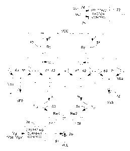
Figure 4 shows the gain control amplifier 31 of the variable gain amplifier
30 shown in Figure 3. In Figure 4, the gain control amplifier includes five
differential circuits and two control circuits.
A first differential circuit includes emitter coupled transistors 41, 43 and a
load resistor 45 connected to the collector of the transistor 41. A second
differential circuit includes transistors 47, 49 and another load resistor 51
connected to the collector of the transistor 49. The resistors 45, 51 have a
resistance Rc. The resistors 45, 51 are connected to a high voltage terminal
of
voltage VCC (e.g., + 5.0 V). The bases of the transistors 43 and 47 are
connected
to each other. A third differential circuit includes transistors 53, 55, the
emitters
of which are coupled through a pair of emitter resistors 57, 59 having a
resistance R~/2. The junction of the resistors 57, 59 is connected to a
current sink
circuit 61. The collector of the transistor 53 is connected to the coupled
emitters
of the transistors 41, 43. The collector of the transistor 55 is connected to
the
coupled emitters of the transistors 47, 49. A fourth differential circuit
includes
emitter coupled transistors 63, 65, the emitters of which are connected to a
current sink circuit 67 which sinks constant current Io. A fifth differential
circuit
includes emitter coupled transistors 69, 71, the emitters of which are
connected
to a current sink circuit 72 which sinks constant current Io. The collectors
of the
transistors 63, 71 are connected to the collectors of the transistors 41, 49,
respectively. The collectors of the transistors 65, 69 are connected to the
high
SUBSTITUTE SHEET (X ULE 16)
CA 02318146 2000-07-13
WO 00/41298 PCT/CA99/01203
7
voltage terminal. The current sink circuits 61, 67, 72 are connected to a low
voltage terminal of voltage VEE (e.g., - 5.0 V). The bases of the transistors
65, 41,
49, 69 are coupled together. The bases of the transistors 63, 43, 47, 71 are
coupled together.
One of the two control circuits is a splitting factor control circuit 73, the
input terminals 74, 75 of which are connected to the collectors of the
transistors
41 and 49 of the first and second differential circuits. In response to a
voltage
difference between voltages V~l and V~2 at the input terminals 74 and 75, the
splitting factor control circuit 73 supplies the base voltage Vba to the bases
of the
transistors 43, 47, 63 and 71. The base voltage Vbb,-constant voltage, is fed
to the
bases of the transistors 41, 65, 49 and 69 by a DC voltage source (not shown)
and
the bases are AC grounded. The control circuit 73 and fourth and fifth
differential circuits perform current split functions to split currents
flowing in
the load resistors 45, 51.
The other control circuit is an operating current control circuit 76 which,
in response to the gain control voltage Vg (differential voltages Vga, Vgb)
from
the peak comparator 37 shown in Figure 3, generates a tail current control
voltage V~sx fed to the current sink circuit 61. The operating current control
circuit 76 controls current Ix flowing in the transistors 53, 55. Current IE
flows in
the collector of each of the transistors 41, 49.
The input differential voltages v;", v~b, which are to be amplified, are fed
to the bases of the transistors 53, 55, respectively. The amplified
differential
voltages vyp, vyb are provided from the bases of the transistors 53, 55 to the
main
amplifier 33.
Figure 5 shows the operating current control circuit 76 which generates
the tail current control voltage V~sx proportional to the gain control voltage
Vg.
In Figure 5, a resistor 77 and a current sink circuit 79 are connected in
series
between the high and low voltage terminals of voltages VCC and VEE. The
junction 80 of the resistor 77 and the current sink circuit 79 is connected to
an
inverting input terminal of an operational amplifier 81, the output terminal
of
which is connected to the base of a transistor 83 of a transistor circuit. The
emitter of the transistor 83 is connected to the low voltage terminal through
a
resistor 85. The collector of the transistor 83 is connected to coupled
emitters of
a pair of transistors 87, 88. The collector of the transistor 88 is connected
to a
non-inverting input terminal of the operational amplifier 81 and connected to
the high voltage terminal through a resistor 89. The resistors 77, 89 have a
resistance Rcc. The resistor 85 has a resistance Rcs.
SUBSTITUTE SHEET (RULE 16)
CA 02318146 2000-07-13
WO 00/41298 PCT/CA99/01203
8
Constant reference current Iref flows in the current sink circuit 79. The
differential gain control voltages Vga, Vgb are fed to the bases of the
transistors
88, 87. The operational amplifier 81 varies the voltage Vcsx which is
proportional of Rcc (Ire f - Icc)~ Icc being current flowing in the resistor
89. The
voltage Vcsx is fed to the transistor 61 of the gain control amplifier shown
in
Figure 4.
Figure 6 shows the splitting factor control circuit 73. In Figure 6, a
voltage divider of two series-connected resistors 91 and 92 is connected
between
the input terminals of the splitting factor control circuit 73. The junction
93 of
the resistors 91 and 92 is connected to an inverting input terminal of an
operational amplifier 94 and to the low voltage terminal through a capacitor
95.
A resistor 97 and a current sink circuit 98 are connected in series between
the
high and low voltage terminals. The junction of the resistor 97 and the
current
sink circuit 98 is connected to a non-inverting input terminal of the
operational
amplifier 94. The resistor 97 has a resistance of aRc and the current of the
sink
circuit 98 is If/a, a being an integer. The output terminal of the operational
amplifier 94 is connected to the bases of the transistors 43, 47, 63 and 71
shown
in Figure 4, so as to vary their base voltage Vba to control the gain of the
gain
control amplifier. The circuit shown in Figure 6 forces the base voltage Vba
such
that the current flowing in the resistors 45, 51 is constant and equal to a
fixed
value I f (I f >_ Ixm;", for maximum gain).
II-2. Operation of the Circuits
In response to the tail current control voltage Vcsx, each of the currents Ix
flowing in the transistors 53, 55 varies linearly between its minimum and
maximum values Im;I, and I~ax as shown in Figure 7. With the minimum
operating current I,n;", the maximum gain G,nax is achieved for the minimum
input voltage vm=n. With the maximum operating current I~ax, the minimum
gain G~ is achieved for the maximum input voltage vmax. When the gain
control amplifier 31 operates at the maximum gain G~,ax, the transistors 41,
65,
49, 69 do not carry any current and the circuit operates as a cascode
amplifier at
the minimum operating current Ia,;r,:
Ix ' I~ - If (3)
SUBSTITUTE SHEET (R ULE 26)
CA 02318146 2000-07-13
WO 00/41298 PCT/CA99/01203
9
The operating current Ix can be optimized to achieve the low equivalent
input noise for the minimum input voltage vmin. For minimum noise, the gain
control amplifier 31 can operate at the maximum gain Gn,ax.
When the amplitude of the input voltage v~ is greater than the maximum
acceptable value for the maximum gain Gn,ax, the operating current Ix
increases
to maintain the linearity of the gain control amplifier 31. The condition for
linearity, for any input signal amplitude v~nx, is similar to equation (1).
Ix x Re >_ v=nx (4)
The operating current Ix has the maximum value Imax at the maximum
input voltage vmax. The gain and operating current variation with the input
signal amplitude for the gain control amplifier 31 is shown in Figure 7. The
gain
and operating current have a linear variation with the input signal amplitude.
Having the maximum gain and the minimum operating current I,n;~,
when the input voltage is very small (signal to nose ratio Iow), allows the
amplifier to operate at the minimum noise and to introduce the minimum signal
to noise ratio degradation. When the input signal amplitude is high (high
signal
to noise ratio) the amplifier will increase the input dynamic range to
maintain
linearity. The power dissipation of the amplifier is a function of the input
voltage amplitude.
If the same circuit is used for following variable gain stages of the main
amplifier 33, the gain and operating current variation with the input signal
is
shown in Figure 8. In the gain control amplifier 31, its gain and the
operation
currenf have a linear variation with the input voltage amplitude.
The voltages at the collectors of the transistors 49 and 41 are symmetrical
and the AC component of the voltage at the inverting input terminal of the
operational amplifier 94 is zero. When the operating current Ix increases
further
than the If value, the base voltage Vba controlling the splitting factor mb
(mb = 1
- m) increases to maintain constant currents flowing in the two resistors 45,
51.
It is assumed that the scaling factor between the pairs of the transistors
(63, 65), (43, 41), (47, 49), (71, 69) is the same and equal to k:1. The
correlation
between the splitting factor m and the operating current Ix is given by:
mIx + (1-m)Io = If
or
SUBSTITUTE SHEET (R ULE 16)
CA 02318146 2000-07-13
WO 00/41298 PCT/CA99/01203
IO
Ix = Io 'f' {If ' Io)/m (5)
Therefore, the current Io must be less than the current If. For (I f - Io)
small
and 0.15 m S 1, the variation of Ix with m is quasi linear.
In order to satisfy the noise factor at the minimum input voltage or over a
given range of minimum voltage amplitudes, it is chosen that the emitter
resistors and the operating current I,~,;n (where I~ 5 I f). The load
resistors 45,
51 result from the maximum gain requirements (10 dB to 15 dB minimum for the
input stage), and power supply operating range. The maximum operating
current Imax ~ vimaxlRe result from the maximum input voltage amplitude for
Linear operation, vtmax and using the value chosen for lZe. The minimum gain
of
the amplifier is determined by the maximum output voltage vya and vyb for
linear operation. To set the minimum gain of the gain control amplifier 31,
the
additional current sources Io of the current sink circuits 67, 72 are:
Io = (If ' Imax x mmin) / {1 - Imin) (6)
The currents Io allow to set the minimum gain G,x,;r, of the amplifier
without affecting the other parameters. In the absence of the current sources
67,
72, the value of If must be changed to satisfy the condition If - {Imax x
mmin) = 0.
This will affect the maximum gain of the amplifier.
Although particular embodiments of the present invention have been
described in detail, it should be appreciated that numerous variations,
modifications, and adaptations may be made without departing from the scope
of the present invention as defined in the claims. For example, the gain
control
amplifier is compatible with a single-ended application. Transistors of a
different type may be used and the current sink circuits may be replaced with
current source circuits.
SUBSTITUTE SHEET (R ULE 16)