Note : Les descriptions sont présentées dans la langue officielle dans laquelle elles ont été soumises.
CA 02319239 2000-09-21
1
MULTI-PORT RANDOM ACCESS MEMORY
TECHNICAL FIELD
The present invention relates to a mufti-port random access
memory.
BACKGROUND ART
Well known RAMs (random access memories) have at least one
address port and include storage elements (core cells). In a paper by A.L.
Silburt et al entitled "A 180-MHz 0.8-um BiCMOS Modular Memory
Family of DRAM and Multiport SRAM", IEEE Journal of Solid-State
Circuits, Vol. 28, No. 3, March 1993, p. 222, at 227 and 228 show various
RAM core arrays.
It is a problem to develop a practical, high-speed, low-power and
area efficient core cell to support multiple ports (e.g., a single high-speed
write port and four high-speed read ports). A conventional five port cell
would have required additional access lines and significant area to achieve
adequate stability margins.
In a paper by G. Gerosa et al entitled "A 2.2 W, 80 MHz Superscalar
RISC Microprocessor", IEEE Journal of Solid-State Circuits, Vol., 29, No.
12, December 1994, p. 1440, at 1447 shows a RAM storage element with
single-ended write access structure. The disclosed structure of five ports
(one write port and four read ports) includes a plurality of transistor
stacks which are connected to respective bit lines. Each transistor stack
has top and bottom MOSFETs (metal oxide semiconductor field effect
transistors). The drain-source circuits of the top and bottom MOSFETs are
series-connected. The gates of the bottom MOSFETs are connected to
respective read port lines. The gates of all top MOSFETs are in parallel
connected to the core cell. This results in unnecessary loading on the bit
line, since the full MOSFET channel capacitance and internal diffusion
capacitance of the top MOSFET in the stack is added to the bit line load for
every core cell storing data which will set the gate of the top MOSFET
"high". This may as implementation described in the paper uses only
CA 02319239 2000-09-21
2
single-ended read access which, for all but the smallest memories, may
result in substantially inferior read performance.
United States Patent No. 5,404,455 granted to D.F. Daly et al on
April 4,1995 discloses a TDM (time division multiplexer) scheme for
alternating communication between a pair of RAMS. In a paper by C.
Ohno entitled "Self-Timed RAM: STRAM", FUJITSU Sci. Tech. J., 24, 4,
December 1988, p. 293 shows a self-timed RAM which has synchronous
operation and an on-chip write pulse generator.
The problem is to develop a practical, high-speed, low-power and
area efficient read port structure to allow multiple (e.g., eight) random
access reads per clock cycle. The straight forward implementation of
multiple physical ports throughout the memory would be prohibitively
complex and inefficient.
In a paper by F.E. Barber et al, "A 2K x 9 Dual Port Memory",
ISSCC Dig. Tech. Papers, Feb. 1985, pp. 44-45 and in a paper by F.E.
Barber et al, "A 200ns 512x10 DUAL PORT RAM", Proc. Electron. Conf.,
vol. 36, Oct. 1982, pp. 380-382 disclose a single port RAM with two
asynchronous address, data and control interfaces. Timing is controlled
by arbitration between address latch enable signals. A memory access
from port A is initiated by asserting the address latch enable signal "low"
on port A, an access from port B is initiated by asserting the address latch
enable signal "low" on port B. If port B attempts to access the memory
while port A is actively accessing the memory, then an arbitration circuit
will delay the port B access until the port A access is complete. In the
RAM, asynchronous enables are used to initiate memory access.
In a paper by T. Matsumura et al, "Pipelined, Time-Sharing Access
Technique for a Highly Integrated Multi-Port Memory", Symp. VLSI
Circuits Dig. Tech. Papers, June 1990, pp. 107-108 and in a paper by K.
Endo et al, "Pipelined, Time-Sharing Access Technique for an Integrated
Multiport Memory", IEEE J. Solid-State Circuits, vol. 26, no. 4, pp. 549-
554, April 1991 disclose a dual port memory with respect to a common
clock (CLK) which is controlled by common write enable (WE) and chip
select (CS) inputs. Likewise, ports 2 and 3 are synchronous with respect to
CA 02319239 2000-09-21
3
a common clock and control inputs. All inputs for ports 0 / 1 are latched
on the rising CLK edge of the port 0 / 1 clock input. All inputs for ports 2
/ 3 are latched on the rising CLK edge of the port 2 / 3 clock input. Port
pairs 0 / 1 and 2 / 3 are time-multiplexed by their respective clock inputs.
Port 0 access is active when the CLK input for ports 0 / 1 is high, port 1 is
active when the same clock input is low. Likewise, port 2 is active when
the CLK input for ports 2 / 3 is high and port 3 is active when the same
clock input is low. Output data is then re-timed in a pipeline cycle and is
presented to the outputs relative to the respective rising clock edge.
Described is a synchronous time-shared access technique that is dependent
on the clock duty cycle (duration of the clock high period and clock low
period) with half of the memory accesses occurring while the clock is high
and the other half occurring while the clock is low.
SUMMARY OF THE INVENTION
It is an object of the present invention to provide an improved
multi-port RAM (random access memory).
In accordance with one aspect of the present invention, there is
provided a multi-port RAM (random access memory) comprising: store
means for storing data, the store means including an array of m rows by n
columns of RAM cells, with N read ports; and addressing means for
generating M address signals of X- and Y-addresses in response to an
input clock signal and an input address signal of address information, the
M address signals being generated during one clock cycle of the input
clock signal and being different in phase from each other, the X- and Y-
addresses of each of the M address signals identifying the row and column
of the array of the RAM cell, respectively.
In an example of the multi-port RAM, the addressing means
comprises clock generating means for generating first and second control
clock signals in response to the input clock signal. It further comprises
address generating means for generating the address signals of the X- and
Y-addresses in response to the first and second control clock signals,
respectively.
CA 02319239 2000-09-21
4
In another example of the mufti-port RAM, the number M of the
address signals is two and the number N of the read ports of the cell is
four. In the RAM, the four read ports are accessed twice per clock cycle.
BRIEF DESCRIPTION OF THE DRAWINGS
An embodiment of the present invention will now be described by
way of example with reference to the accompanying drawings in which:
Figure 1 shows the structure of Figures 1A -1D which illustrate a
mufti-port RAM (random access memory) according to an embodiment of
the present invention;
Figure 1A is a block diagram of an X-address circuit and a row
decode circuit which are included in the mufti-port RAM;
Figure 1B is a block diagram of a mufti-port core cell array which is
included in the mufti-port RAM;
Figure 1C is a block diagram of a Y-address circuit, a column
decode circuit and a clock generator which are included in the mufti-port
RAM;
Figure 1D is a block diagram of a bit line access circuit and a data
output circuit which are included in the mufti-port RAM;
Figure 2 is a detailed circuit diagram of a RAM cell included in the
mufti-port core cell array shown in Figure 1B;
Figure 3 is a detailed diagram of a latch included in the RAM cell
shown in Figure 2;
Figure 4 is a detailed block diagram of the clock generator shown in
Figure 1C;
Figure 5 is a detailed circuit diagram of the reset generators shown
in Figure 4;
Figure 6 is a timing chart which illustrates the operation of the
RAM cell shown in Figure 2; and
Figure 7 is a timing chart which illustrates the operation of the
mufti-port RAM.
DETAILED DESCRIPTION
I. Entire Structure of an Embodiment RAM
CA 02319239 2000-09-21
The entire structure of a mufti-port RAM (random access memory)
of an embodiment according to the present invention will now be
described.
5 Referring to Figures lA -1D, a mufti-port RAM has a core cell array
110 of m (=48) rows by n (=64) columns with one write port and four read
ports. The core cell array 110 is connected to word lines 112 and bit lines
114. Control circuits for the write port are not shown. Each RAM cell of
the core cell array 110 is a dynamic or static storage element. The word
lines 112 are connected to the row decode circuit 116. The address
identifying the core cell for data reading in the core cell array 110 is
determined by X- and Y-address signals which are provided by a row
decode circuit 116 and a column decode circuit 118, respectively.
The row decode circuit 116 has 192 row decoders (4 ports per row,
48 rows). T'he bit lines 114 are connected to a bit line access circuit 120
which has 256 column access circuits (4 ports per column, 64 columns; 8
columns per bit, 4 data buses per bit). The address data is contained in an
address signal which is present on an address input bus 122, the address
signal having X- and Y-address data. The address input bus 122 is an 8
port x 9-bit address input bus. The 8 ports are represented by "a" - "h".
The Y-address data is fed to a Y-address circuit 124 via an 8 port (ports a -
h) x 3 bit (bits 0 - 2) bus. The X-address data is fed to an X-address circuit
126 via an 8 port (ports a - h) x 6 bit (bits 3 - 8) bus.
The Y-address circuit 124 has 24 Y-address registers (3 Y-address
inputs per port, 8 ports). The X-address circuit 126 has 48 X-address
register and predecoders (8 ports, 6 X-address inputs per port; 2-to-4
predecode per port). The X-address circuit 126 is connected to the row
decode circuit 116 via a predecoded row address bus 128. The Y-address
circuit 124 is connected via a column address bus 130 to the column
decode circuit 118 which is connected to the bit line access circuit 120 via a
decoded column address bus 132 having decoded Y-address lines. The
column decode circuit 118 has 32 column decoders (8 per port pair, 4 port
pairs (a/e, b/f, c/g, d/h); 3-to-8 decode per port pair).
CA 02319239 2000-09-21
6
Timing of addressing is controlled by a clock generator 134 which is
a self-timed, time multiplex control circuit. A clock input line 136 to which
a system clock signal ck is fed by a clock source (not shown) is connected
to the clock generator 134. Also, a mode line 138 to which a self-timing
override mode signal stow is fed by a signal source (not shown) is
connected to the clock generator 134. The clock generator 134 generates
clock signals of two phases H1 and 02 and doubles the frequency of the
clock signal by multiplexing. Multiplex control clock signals crxl and crx2
from the clock generator 134 are fed to the row decode circuit 116 via
multiplex clock lines 140 and 142, respectively. Interface clock signals cril
and cri2 from the clock generator 134 are fed to both the Y-address circuit
124 and the X-address circuit 126 via interface clock lines 144 and 146,
respectively. Multiplex control clock signals cryl and cry2 from the clock
generator 134 are fed to the column decode circuit 118 via multiplex clock
lines 148 and 150, respectively.
A o1 precharge clock signal crpl and a rat precharge clock signal
crp2 are provided by the clock generator 134 to the bit line access circuit
120 via precharge lines 152 and 154, respectively. A of sense amp latch
clock signal crll, a 02 sense amp latch clock signal crl2 and an output
register clock signal crq are provided by the clock generator 134 to a data
output circuit 156 via a sense clock line 158, a sense clock line 160 and a
register clock line 162, respectively. The data output circuit 156 has 64
sense amplifiers (8 per output port, 8 output ports,) and is connected to an
8 port x 8-bit data output bus. The data buses 164 from the bit line access
circuit 120 are connected to the data output circuit 156.
II. Detailed Structure of Circuits of the RAM
The following description assumes, for simplicity and purely by
way of example, that FETs (field effect transistors) referred to are
MOSFETs (metal oxide semiconductor FETs) and a supply voltage +Vcc is
+5.0 volts.
(i) Multi-Port RAM Cell Array
CA 02319239 2000-09-21
7
The multi-port RAM cell array shown in Figure 1B will now be
described. Each RAM cell of the multi-port RAM cell array consists of
four differential read ports with indirect data access via gated, bit line
pull-down transistors and one single-ended write-only port with local bit
line inversion to give pseudo-differential write access.
Each RAM cell of the multi-port RAM cell array has a five-port
storage element (core cell) and includes one write port and four
differential read ports with indirect data access. The RAM cell includes a
latch 210 which has two inverters 211 and 212. Each of the inverters 211
and 212 has a CMOS (complementary MOS) inverter. The input and the
output terminals of the inverter 211 are connected to the output and the
input terminals of the inverter 212, respectively.
The source of a FET 214 is connected to the drain of a FET 216 and
the source of a FET 218 is connected to the drain of a FET 220. Similarly,
the source of a FET 222 is connected to the drain of a FET 224 and the
source of a FET 226 is connected to the drain of a FET 228. The source of a
FET 230 is connected to the drain of a FET 232 and the source of a FET 234
is connected to the drain of a FET 236. The source of a FET 238 is
connected to the drain of a FET 240 and the source of a FET 242 is
connected to the drain of a FET 244.
The output terminal of the inverter 211 and the input terminal of
the inverter 212 are connected to the gates of the FETs 216, 224, 232 and
240 and the drain of a FET 246. The input terminal of the inverter 211 and
the output terminal of the inverter 212 are connected to the gates of the
FETs 220, 228, 236 and 244 and the drain of a FET 248 whose source is
connected to the drain of a FET 250. The sources of the FETs 216, 220, 224,
228, 232, 236, 240, 244 and 250 are connected to the ground terminal.
The gates of the FETs 246 and 248 are connected to a line 252 on
which a write word line signal wlw is present. The gate of the FET 250
and the source of the FET 246 are connected to a line 254 on which a write
bit line signal blw representing data "zero" or "one" is present.
CA 02319239 2000-09-21
8
A line 256 on which a word line read signal wlra is present is
connected to the gates of the FETs 214 and 218. A line 258 on which a
word line read signal wlrb is present is connected to the gates of the FETs
222 and 226. A line 260 on which a word line read signal wlrc is present is
connected to the gates of the FETs 230 and 234. A line 262 on which a
word line read signal wlrd is present is connected to the gates of the FETs
238 and 242.
The drains of the FETs 218, 226, 234 and 242 are connected to bit
lines 264, 266, 268 and 270, respectively, on which read bit line signals
blra,
blrb, blrc and bird are present. The drains of the FETs 214, 222, 230 and
238 are connected to bit lines 272, 274, 276 and 278, respectively, on which
read bit line signals blrna, blrnb, blrnc and blrnd are present. The bit lines
264 and 272, 266 and 274, 268 and 276, 270 and 278 are pairs of bit lines
and on the respective pairs, the read bit line signals blra and blrna, blrb
and blrnb, blrc and blrnc, and bird and blrnd are which are differential
signals are present.
Figure 3 shows a detail of the latch 210 of the multi-port RAM cell
array. The latch 210 is a well known RAM storage element which includes
two CMOS inverters. In Figure 3, the drains of a P-channel FET 280 (a
load device) and an N-channel FET 282 (a drive device), which define one
CMOS inverter, are connected to the gates of a P-channel FET 284 (a load
device) and an N-channel FET 286 (a drive device), which define the other
CMOS inverter. Similarly, the drains of the FETs 284 and 286 are
connected to the gates of the FETs 280 and 282. The sources of the FETs
280 and 284 are connected to the voltage terminal of the supply voltage
+Vcc. The sources of the FETs 282 and 286 are connected to the ground
terminal. The junction of the drains of the FETs 280 and 282 defines node
CN. The junction of the drains of the FETs 284 and 286 defines node C.
Nodes CN and C are data input and output terminals of the latch 210.
(ii) Clock Generator
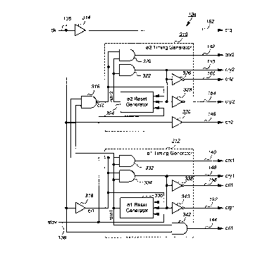
Referring to Figure 4 which shows the clock generator 134 in detail,
it has a o2 timing generator 310, a e1 timing generator 312, a buffer 314, a
NAND gate 316 and a buffer 318. The clock input line 136 to which the
CA 02319239 2000-09-21
9
system clock signal ck is fed is connected to the H2 timing generator 310
and the r~1 timing generator 312 and to input terminals of the buffers 314
and 318. The mode line 138 to which the self-timing override mode signal
stow is fed is connected to the a2 timing generator 310 and the e1 timing
generator 312. The buffer 314 delays the system clock signal ck and
provides the output register clock signal crq on the register clock line 162.
The buffer 318 delays the system clock signal ck and provides a e~1 read
clock signal crl. The output terminal of the buffer 318 is connected to the
e1 timing generator 312 and the NAND gate 316. The e2 timing generator
310 has two AND gates 320 and 322, a e2 reset generator 324, two
inverters 326 and 328 and a buffer 330.
The e1 timing generator 312 has two AND gates 332 and 334, a e1
reset generator 336, two inverters 338 and 340 and an AND gate 342. The
clock input line 136 is connected to the buffer 330 and the AND gate 342.
The buffer 330 delays the system clock signal ck and provides the interface
clock signal cri2 on the interface clock line 146. The output terminal of the
buffer 318 is connected to the NAND gate 316, the AND gate 332, the
AND gate 334 and the of reset generator 336. The output terminal of the
NAND gate 316 is connected to the AND gates 320 and 322 and the a~2
reset generator 324. The output terminal of the AND gate 322 is connected
to the a2 reset generator 324 and the inverters 326 and 328. The output
terminal of the AND gate 334 is connected to the H1 reset generator 336
and the inverters 338 and 340.
The self-timing override mode signal stow is fed to the 01 and the e2
reset generators 336 and 324. The override mode signal stow is a
diagnostic mode control input signal and it is "high" and "low" in normal
and diagnostic modes, respectively.
The e1 reset generator 336 provides a e1 reset control signal rstnl
on its output terminal which is connected to the NAND gate 316 and the
AND gates 332, 334 and 342. The NAND gate 316 provides a e2 read clock
signal cr2 which is a NAND logic signal of the a1 read clock signal cr1 and
the a1 reset control signal rstnl. The a2 reset generator 324 provides a e2
reset control signal rstn2 on its output terminal which is connected to the
AND gates 320 and 322. The AND gate 320 provides the multiplex control
CA 02319239 2000-09-21
clock signal crx2 on the multiplex clock line 142. The multiplex control
clock signal crx2 is an AND logic signal of the e~2 read clock signal cr2 and
the cr2 reset control signal rstn2. The AND gate 322 provides the multiplex
control clock signal cry2 on the multiplex clock line 150. The multiplex
5 control clock signal cry2 is an AND logic signal of the 02 read clock signal
cr2 and the 02 reset control signal rstn2. The inverter 326 provides the a2
sense amp latch clock signal crl2 on the sense clock line 160. The 02 sense
amp latch clock signal crl2 is an inverted signal of the multiplex control
clock signal cry2. The inverter 328 provides the e2 precharge clock signal
10 crp2 on the precharge line 154. The o2 precharge clock signal crp2 is an
inverted signal of the multiplex control clock signal cry2. The AND gate
332 provides the multiplex control clock signal crxl on the multiplex clock
line 140. The multiplex control clock signal crxl is an AND logic signal of
the o1 read clock signal crl and the m1 reset control signal rstnl. The AND
gate 334 provides the multiplex control clock signal cryl on the multiplex
clock line 148. The multiplex control clock signal cryl is an AND logic
signal of the o1 read clock signal crl and the a1 reset control signal rstnl.
The inverter 338 provides the a~1 sense amp latch clock signal crll on the
sense clock line 158. The a1 sense amp latch clock signal crll is an inverted
signal of the multiplex control clock signal cryl. The inverter 340 provides
the o1 precharge clock signal crpl on the precharge line 152. The e1
precharge clock signal crpl is an inverted signal of the multiplex control
clock signal cryl. The AND gate 342 provides the interface clock signal
cril on the interface clock line 144. The interface clock signal cril is an
AND logic signal of the system clock signal ck and the a1 reset control
signal rstnl.
(iii) Reset Generator
Figure 5 is a detailed circuit diagram of the e2 reset generator 324
and the a1 reset generator 336 which have an identical circuit. In Figure 5,
each of the generators 324 and 336 is a self-timing reset generator having a
NAND gate 410, an inverter 412, a P-channel FET 414, an N-channel FET
416 and an inverter 418. The input terminals of the NAND gate 410 are
connected to lines comprised in a set input bus 420 to which the read clock
signal cr (the o1 or e2 read clock signals crl or cr2), the multiplex control
clock signal cry (the multiplex control clock signals cryl or cry2) and the
CA 02319239 2000-09-21
11
override mode signal stow are provided. The input terminal of the
inverter 412 is connected to a reset input line 422 to which the read clock
signal cr is provided. The output terminal of the NAND gate 410 is
connected to the gate of the P-channel FET 414, the source of which is
connected to the voltage supply terminal of a positive voltage +Vcc. The
output terminal of the inverter 412 is connected to the gate of the N-
channel FET 416, the drain and source of which are connected to the drain
of the P-channel FET 414 and the ground terminal, respectively. The
drains of the FETs 414 and 416 are connected to an input terminal of the
inverter 418 which provides a reset control signal rstn (the o1 or the 02
reset control signals rstnl or rstn2).
III. Operation of the Embodiment
(i) Multi-Port RAM
Figure 6 is a timing chart which illustrates the operation of the
RAM cell shown in Figure 2. Operation of the mufti-port RAM cell array
will now be described with reference to Figures 2, 3 and 6.
Write Mode
The write access port of the embodiment mufti-port RAM cell array
is single-ended. A single-ended write port is desirable to reduce write
power and may eliminate, for example, 50% of the write bit lines from the
core array as compared to traditional differential writes.
The FET 246 provides the traditional single-ended N-channel access
to node C, resulting in high-speed write access for writing data "zero".
The FET 246 is easily margined for high-speed writing against the weak P-
channel pull-up FET 284 since it is in common-source mode. However, the
FET 246 has insufficient drive to write data "one" into the latch 210 (i.e.,
node C "high"), since it would be in the source-follower pull-up mode (by
the FET 286) where drive capability is significantly reduced. Margining of
the N-channel pull-down FET 286 in the latch 210 versus the FET 246 is not
feasible for high-speed write access. To achieve the high-speed write to
data "one", a pseudo bit line inversion is applied through the FETs 248 and
CA 02319239 2000-09-21
12
250 to pull node CN towards ground, when both the write bit line signal
blw on the line 254 and the write word line signal wlw on the line 252 are
"high". The FET 248 acts as the write access device, while the FET 250
gates the pull-down of node CN, when the write bit line signal blw on the
line 254 contains data "one". In spite of the weak P-channel pull-up in the
latch 210, since the FETs 248 and 250 connected in series thereto are in
common-source mode, the latch 210 write speed is improved.
(a) Write a "zero" (Figure 6 (a)):
In the embodiment multi-port RAM cell array, when data "zero" or
"one" is required to be written into the latch 210, the write word line signal
wlw on the line 252 is "high". In a case of data "zero", the write bit line
signal blw on the line 254 is "low". In response to "high" at the write word
line signal wlw, the FET 246 becomes conductive and node C is pulled-
down to "low" through the on FET 246. In response to the pull-down at
node C, node CN is pulled-up by the FET 280. Therefore, the FET 286
becomes on, causing node C to maintain "low".
(b) Write a "one" (Figure 6 (b)):
In a case of data "one", the write bit line signal blw on the line 254 is
"high". In response to "high" at the write word line signal wlw and the
write bit line signal blw, the FETs 248 and 250 become conductive and
node CN is pulled-down towards the ground level ("low"). In response to
the pull-down at node CN, node C is pulled-up by the FET 284. Therefore,
the FET 282 becomes on, causing node CN to maintain "low".
Read Mode
The read access port of this embodiment of the mufti-port RAM cell
array is differential. The indirect read data access scheme consists of the
FETs 214, 216, 218 and 220. It supports a large number of parallel read
ports without incurring the stability problems of traditional pass-transistor
access cells, since there is never any direct access from the read bit lines
(on which a differential read bit line signals blr and blrn are present) to
the
data storage nodes (C and CN). Thus, the cell is inherently stable under all
CA 02319239 2000-09-21
13
read conditions and need only be margined to meet the write access and
soft-error immunity criteria.
(a) Read a "zero" (Figure 6 (c)):
While the latch 210 stores data "zero", nodes CN and C are "high"
and "low", respectively. While the word line read signal wlra on the line
256, for example, is "high", the FETs 218 and 214 are gated. In response to
"high" at node CN, the FETs 220 and 218 become on and the bit line 264 is
pulled-down by the on FETs 220 and 218, with the result that the read bit
line signal blra becomes "low". Because node C is "low", the FETs 216 and
214 are off and the read bit line signal blrna on the line 272 is "high".
Hence, by the gating and pull-down functions of the FETs, data "zero" is
read.
Similarly, while the word line read signal wlrb on the line 258 is
"high", the FETs 226 and 222 are gated. In response to "high" at node CN,
the FETs 228 and 226 become conductive and the bit line 266 is pulled-
down by the on FETs 228 and 226, with the result that the read bit line
signal blrb becomes "low". Because node C is "low", the FETs 224 and 222
are nonconductive and the read bit line signal blrnb on the line 274 is
"high". Hence, differential data "zero" is read between the bit lines 266 and
274.
(b) Read a "one" (Figure 6 (d)):
While the latch 210 stores data "one", nodes CN and C are "low" and
"high", respectively. While the word line read signal wlra on the line 256,
for example, is "high", the FETs 218 and 220 are gated. In response to
"high" at node C, the FETs 216 and 214 become on and the bit line 272 is
pulled-down, with the result that the read bit line signal blrna becomes
"low". Because node CN is "low", the FETs 220 and 218 are off and the
read bit line signal blra on the line 264 is "high". Hence, by the gating and
pull-down functions of the FETs, data "one" is read.
Similarly, while the word line read signal wlrb on the line 258 is
"high", the FETs 226 and 222 are gated. In response to "high" at node C,
CA 02319239 2000-09-21
14
the FETs 224 and 222 become conductive and the bit line 274 is pulled-
down, with the result that the read bit line signal blrnb becomes "low".
Because node CN is "low", the FETs 228 and 226 are nonconductive and
the read bit line signal blrb on the line 266 is "high". Hence, differential
data "one" is read between the bit lines 274 and 266.
(ii) Multi-Port RAM
Figure 7 is a timing chart which illustrates the operation of the
mufti-port RAM. Operation of the embodiment will now be described
with reference to the drawings.
Read Port Access
Time multiplexing is employed in order to create eight data
accesses from the four physical read ports in the RAM cell array 110.
Every read cycle is divided into two phases: phase 1 (01) and phase 2 (02).
Phase 1 (01) accesses provide data for four ports a - d. Phase 2 (02)
accesses provide data for four ports a - h. The multiplexed read
architecture can be seen clearly through the convergence of the port
address signal paths on the core, and the divergence of the four data paths
in the sense amplifier and output stages.
The eight read ports are fully synchronous with respect to the
single clock of the system clock signal ck which is present on the clock
input line 136. An internal self timing mechanism is employed to generate
the time multiplex control signals with minimum average power
dissipation, regardless of the read clock frequency, duty-cycle, process or
operating conditions.
The self-timed, time multiplex control signal timing sequence is
shown in Figure 7. Operation of a complete cycle is described below with
all steps associated with the time division multiplex read port function.
The rising edge of the system clock signal ck triggers the output
register clock signal crq. In response to the output register clock signal crq
which is provided in the register clock line 162, the read data path output
CA 02319239 2000-09-21
from the previous cycle is registered in the data output circuit 156. The
rising edge of the system clock signal ck initiates the two interface clock
signals cril and cri2 to latch the eight port address inputs. The interface
clock signal cril is provided by the e1 timing generator 312 to the X-
5 address circuit 126 and the Y-address circuit 124 via the interface clock
line
144. The interface clock signal cri2 is provided by the a2 timing generator
310 to the X-address circuit 126 and the Y-address circuit 124 via the
interface clock line 146.
10 The rising edge of the system clock signal ck initiates the multiplex
control clock signals crxl and cryl, which are provided by the ral timing
generator 312 to the row decode circuit 116 and the column decode circuit
118 via the multiplex clock lines 140 and 148, respectively. In response to
the multiplex control clock signal crxl, the r~1 X-addresses (wlr) are
15 selected by the row decode circuit 116. The selected m1 X-addresses are
provided to the word lines 112. Similarly, in response to the multiplex
control clock signal cryl, the a1 Y-addresses (ypr) are selected by the
column decode circuit 118. The selected 01 Y-addresses are provided to
the decoded column address bus 132. This accomplishes the e1 row and
column select function. The rising edge of the system clock signal ck sets
the e2 reset control signal rstn2, thereby arming the 02 clock generation
circuitry for subsequent generation of the e1 reset.
The rising edge of the multiplex control clock signal cryl triggers
the e1 sense amp latch clock signal crll to provide equalization and data
access and to re-time o1 and e2 data from the previous cycle. The internal
self-timing loop feedback path then causes a falling edge on the e~1 reset
control signal rstnl. The falling edge of the a1 reset control signal rstnl
resets the multiplex control clock signals crxl and cryl. In response to the
reset, the port a-d predecoded address lines are reconnected to the address
input path and the e1 row and column addresses are deselected from the
word lines 112 and the decoded Y-address lines of the decoded column
address bus 132.
The falling edge of the multiplex control clock signal cryl resets the
01 sense amp latch clock signal crll to initiate latching and the 01
CA 02319239 2000-09-21
16
precharge clock signal crpl to equalize the data bus and bit lines for the
subsequent o2 read.
The falling edge of the e1 reset control signal rstnl initiates the e2
cycle by enabling the armed multiplex control clock signals crx2 and cry2.
The rising edges of the multiplex control clock signal crx2 and the
multiplex control clock signal cry2 gate the e2 X-addresses to the word
lines 112 and the rat Y-addresses to the decoded Y-address lines. This
accomplishes the 02 row and column select function. The rising edge of
the multiplex control clock signal cry2 triggers the e2 sense amp latch
clock signal crl2 to provide equalization and data access. The internal self-
timing loop feedback path then causes a falling edge on the a2 reset
control signal rstn2.
The falling edge of the r~2 reset control signal rstn2 resets the
multiplex control clock signals crx2 and cry2. In response to the reset, the
port e-h predecoded address lines are reconnected to the address input
path and the e2 row and column addresses are deselected from the word
lines 112 and decoded Y-address lines. The falling edge of the multiplex
control clock signal cry2 resets the 02 sense amp latch clock signal crl2 to
initiate latching and the 02 precharge clock signal crp2 to equalize the data
bus and bit lines for the subsequent e1 read. The falling edge of the
system clock signal ck resets the e1 reset control signal rstnl, thereby re-
arming the e1 clock generation circuitry for subsequent generation of the
next rising clock cycle.
In response to the X- and Y-addresses, the data stored in the cell in
the row and column is read. For example, while the word line read signal
wlra on the line 256 is "high", the FETs 218 and 214 are gated. A "zero" or
"one" data stored in the latch 210 is read through the FETs 220, 218 and
216, 214 between the read bit lines 264 and 272.
Self-timed, Time Multiplex Control
Self-timed, time multiplex control signals are provided by the clock
generator 134 which is shown in detail in Figure 4. In the clock generator
134, there are two self timing loops controlling the time multiplexed
CA 02319239 2000-09-21
17
operations. The first loop, which is for the o1 timing generation and reset
and includes the signal paths of the a1 read clock signal crl, the multiplex
control clock signal cryl and the o1 reset control signal rstnl (a of self-
timing loop), includes the path of the AND gate 334 ~ the 01 reset
generator 336. The second loop, whose operation is triggered by the first
through the NAND gate 316, is for the e2 timing generation and reset.
The second loop includes the paths of the 02 read clock signal cr2, the
multiplex control clock signal cry2 and the a2 reset control signal rstn2
and the path of the AND gate 322 ~ the 82 reset generator 324.
Operation of the timing loop is as follows. It is assumed that the
system clock signal ck is "low". A new cycle is about to be initiated and
the override mode signal stow is "high". In this case, the al read clock
signal crl is "low" and the 02 read clock signal cr2 is "high". This causes
the H2 reset control signal rstn2 to be "lov~i' and the e1 reset control
signal
rstnl to be "high". The "high" level on the e1 reset control signal rstnl
arms the AND gates 332 and 334 which are in the a1 clock paths. The
"low" level on the e2 reset control signal rstn2 disarms the AND gates 320
and 322 and the 02 clock paths. The multi-port RAM is now in a "ready
state" for the cycle to begin.
On the rising edge of the system clock signal ck, the interface clock
signals cril and cri2 fire to latch the interface data in the address
registers
and sequence the e1 interface operation. The multiplex control clock
signals crxl and cryl, the 01 sense amp latch clock signal crll and the o1
precharge clock signal crpl all fire to sequence the x-decode, the y-decode
and the data path operation. The 01 self-timing loop is also triggered and
the rising edge of the multiplex control clock signal cryl feeds back
through the H1 reset generator 336, forcing the 01 reset control signal rstnl
"low". The falling edge of the a1 reset control signal rstnl shuts down all
e1 clocks ending the 01 cycle. The 01 reset generator has a tuned delay
which allows all 01 operations to complete before shut down.
The rising edge of the system clock signal ck also causes the o2 read
clock signal cr2 to fall, since the a~1 reset control signal rstnl is "high".
The
falling edge of the o2 read clock signal cr2 will cause the 02 reset generator
CA 02319239 2000-09-21
18
324 to be cleared and the e2 reset control signal rstn2 will go "high",
arming the 02 clock path.
The falling edge of the a~1 reset control signal rstnl is used as the
trigger to start the a2 timing generator 310 via the NAND gate 316. The
falling edge of the a1 reset control signal rstnl causes the a2 read clock
signal cr2 to rise. It causes all 02 clocks, the multiplex control clock
signals
crx2 and cry2, the a2 sense amp latch clock signal crl2 and the e2
precharge clock signal crp2 to transit their state. As with e1, the rising
edge of the multiplex control clock signal cry2 feeds back through the e2
reset generator 324, forcing the a2 reset control signal rstn2 "low". The
falling edge of the e2 reset control signal rstn2 shuts down all 02 clocks
ending the 02 cycle.
Additional multiplex phases may be added following the s2
circuitry with the 02 read clock signal cr2 and the e~2 reset control signal
rstn2 feeding the 03 timing generator, etc.
The falling edge of the system clock signal ck will once again force
the e1 reset control signal rstnl "high" in preparation for the next cycle. It
should be noted that the minimum system clock signal ck "high" period is
limited by the length of the e1 cycle. That is, the system clock signal ck
should not be taken "low", before the gal reset control signal rstnl goes
"low" or the of cycle may be corrupted.
Self-Timing Override
A self-timing override mode is provided for the two phase version
of the control circuit. By asserting the override mode signal stow "low", the
reset circuit operation is disabled and the e1 and the e2 reset control
signals rstnl and rstn2 are latched in a "high" state. One rising clock edge
is required to force the a2 reset control signal rstn2 "high", once the
override mode signal stow is asserted, the al reset control signal rstnl is
set "high" during the system clock signal ck "low" and remains "high" until
the override mode signal stow is released.
CA 02319239 2000-09-21
19
With both the e1 and the e2 reset control signals rstnl and rstn2
"high", both the ml and e2 clock paths are armed. The o1 clocks fire on the
rising edge of the system clock signal ck and the e2 clocks fire on the
falling edge. This allows the e1 and the e2 cycles to be controlled
externally by the duty cycle of the clock for test and debug purposes. This
function is not scalable to more phases than two in the embodiment, since
the clock input has only two phases.
The innovative feature of the mufti-port RAM is the self-timed, time
multiplexed read port control which allows the eight read ports to be
implemented as four physical port structures accessed twice per clock
cycle. No special control or clocking is required externally to the memory
since all timing is internally generated from the single rising clock
transition. In the mufti-port RAM, all ports are fully synchronous with
respect to a single clock input. No arbitration between ports is required,
since the timing generator has a fixed sequence. The clock must only be
"high" or "low" for minimum periods set by the control circuit. The actual
timing of the memory operation is generated by the self-timed control
circuitry which only requires the rising clock edge as a trigger. Once
initiated, the self-timed circuitry completes the M accesses as quickly as
possible (in sequence) and then disables the memory in preparation for the
next cycle. This technique has two major advantages: 1) the architecture is
scalable to many self-timed access phases (M > 2) and 2) the memory shut-
down at faster process conditions significantly reduces power
consumption, since the circuit is only active for as long as needed to
complete the function.
Advantageously, the mufti-port RAM is scalable. Although it has
been implemented for an eight port function where four physical ports are
time multiplexed to give an eight port function there is no reason, for
example, that a three port function could not be realized from one physical
port if three cycles of multiplexing were used. Any number of timing
phases may be added in sequence.
The row and column identification implemented into the read-port
may be applied to the control circuits for the write port also. In such a
write-port implementation, the address identifying the core cell for data
CA 02319239 2000-09-21
storing in the core cell array 110 is determined by X- and Y-address signals
which are provided by the row decode circuit 116 and the column decode
circuit 118, respectively. Furthermore, the row and column identification
may be implemented into both the read-port and the write-port and the
S core cells for data storing and reading in the core cell array 110 are
determined by X- and Y-address signals.
Although particular embodiments of the present invention have
been described in detail, it should be appreciated that numerous
10 variations, modifications, and adaptations may be made without
departing from the scope of the present invention as defined in the claims.
For example, the data storage element may include various dynamic and
static RAM core cells.