Note : Les descriptions sont présentées dans la langue officielle dans laquelle elles ont été soumises.
CA 02320857 2000-08-18
WO 99/42799 PCT/US99/03489
-1
Gross Reference To Related A~nlications
This application claims the benefit of prior filed co-pending provisional
application entitled,
"Silicon On Insulator Strain Gage," Serial No. 60/075,135, filed February 18,
1998.
Background Of The Inve~,stion
1. Field Of The Invention
The present invention relates generally to the field of strain measurement.
More particularly,
Io the present invention relates to using semiconductive strain gages to
measure strain on an object.
When force is applied to an object, this results in stress on the object.
Stress is the force per
unit area acting on the object. When an object experiences stress, the object
will experience
deformation, which is the change in shape of the object in any dimension.
Strain is a measurement
of the intensity of this deformation. More specifically, strain is the
deformation per unit length of
the object in any dimension resulting from stress.
Devices employing a variety of techniques are available to measure strain on
an object.
Typically, these devices translate the mechanical strain on an object into an
electrical signal. Strain
gages are commonly used in such devices.
One type of conventional strain gage consists of a monolith of conductive or
semiconductive
material whose resistance changes when the gage deforms. Typically, this type
of conventional
strain gage is mechanically bonded to a mechanical sensor with an adhesive to
form a strain gage
assembly. Specifically, as illustrated in FIG. 1, an adhesive is applied to
the mechanical sensor 2
to form an adhesive layer 3, the strain gage 4 is pressed against the adhesive
layer 3, and the
adhesive layer 3 is allowed time to cure. It should be noted that FIG. 1 is
not drawn to scale. The
adhesive may be an epoxy, paste or other suitable bonding compound or agent.
In operation, when a force impacts on the mechanical sensor 2, the resultant
deformation of
the mechanical sensor 2 causes the strain gage 4 to similarly deform, with a
resultant change in
3o electrical resistance. This change in resistance is measured and used to
provide a measurement of
the strain on the mechanical sensor 2. This change in resistance may also be
used to determine the
stress or pressure on the mechanical sensor 2. Force cells, loads cells,
pressure transducers and
CA 02320857 2000-08-18
WO 99/42799 PCTIUS99/03489
-2
accelerometers are typical devices that make use of this principle.
The material of the strain gage 4 can be a conductive metal or a
semiconductive material.
Semiconductive materials have the advantage of providing a larger change in
resistance for a given
change in strain than do conductive metals. In a strain gage assembly 1,
attaching a strain gage 4
of semiconductive material to a mechanical sensor 2 of metal material may
result in electrical shorts
or electrical leakage during operation. Specifically, shorts and leakage
result when the adhesive
layer 3 is too thin or unevenly applied. Subsequently, when the strain gage 3
is pressed against the
mechanical member 2 and the adhesive is allowed to cure, the strain gage 4 may
actually contact the
mechanical member 2 at points, resulting in a short circuit between the
mechanical sensor 2 and the
1 o strain gage 4.
If the adhesive layer 3 is too thin at a certain point, current will leak
across the adhesive layer
3 when a sufficient voltage potential exists between the mechanical sensor 2
and the strain gage 4.
The voltage at which leakage will occur is the dielectric breakdown voltage of
the adhesive layer 4.
To prevent electrical shorts and electrical leakage, the strain gage 4 must be
better insulated
from the mechanical sensor 2. Initially, this involves choosing an insulating
adhesive as opposed
to a non-insulating adhesive. Conventionally, to achieve improved insulation,
a filled adhesive is
chosen to make the adhesive layer. The filler of a filled adhesive is
typically a granular substance
such as a fine powder. The purpose of using a filled adhesive is to increase
the thickness of the
adhesive layer 3. Increasing the thickness of the adhesive layer 3 produces a
higher dielectric
breakdown voltage of the adhesive layer 3. Since the breakdown voltage is
higher, there is less
likelihood of electrical leakage across the adhesive layer 3.
Although using a filled adhesive produces a higher dielectric breakdown
voltage, the
application of only one coat of filled adhesive does not provide a high enough
dielectric breakdown
voltage in the adhesive layer to avoid electrical shorts and electrical
leakage.
Conventionally, to further improve insulation, two coats of the filled
adhesive are applied
to produce the adhesive layer 3. FIG. 2 is a perspective side view of a
section 9 of the strain gage
assembly 1 of FIG. 1 that shows in further detail the adhesive layer 3. The
adhesive layer 3 includes
a pre-coat 5 and a gage coat 6. During manufacturing, the pre-coat 5 of filled
adhesive is applied
to the mechanical sensor 2 and allowed time to cure. Next, the gage coat 6 of
filled adhesive is
applied to the pre-coat 5, the strain gage 4 is pressed against the gage coat
6, and the gage coat 6 is
allowed time to cure. Adding the extra coat assures that the adhesive layer 3
is sufficiently thick to
avoid electrical shorts and electrical leakage. Typically, the pre-coat 5 and
gage coat 6 are of the
CA 02320857 2000-08-18
WO 99/42799 PCT/US99103489
-3
same or similar adhesive material. The thickness of the adhesive layer 3 is
represented in FIG. 2 by
ta.
A conventional strain gage assembly 1 of FIG. 2 that uses a strain gage 3 of
semiconductive
material has an adhesive Iayer 3 with a thickness to of approximately 1.0 mil
(25.4 ,um). The
dielectric strength of a material is the voltage potential at which dielectric
breakdown will occur per
unit length of the material. For filled adhesives typically used for the
strain gage assembly 3 of FIG.
2, the dielectric breakdown of the filled adhesive is approximately 250 Volts
per mil (250 V/mil;
9.84 V/,um). Therefore, the typical dielectric breakdown voltage of the
adhesive layer 3 is
approximately 250 Volts (250 V/mil X 1.0 mil).
to Using a filled adhesive and adding a second coat of adhesive increases the
thickness of the
adhesive layer 3. Although increasing the thickness produces a higher
dielectric breakdown of the
adhesive layer 3, as the thickness of the adhesive layer 3 increases,
mechanical performance can
decrease. Furthermore, the fillers of filled adhesives can reduce the strength
of the adhesive. The
filler within the adhesive may have inconsistent granule size and this can
make it more difficult for
the adhesive layer 3 to bond the strain gage 4 to the mechanical member 2,
create high stress points
in the strain gage 4, and introduce possible voids between the strain gage 4
and the adhesive layer
3.
When choosing an adhesive, one wants an adhesive with the best combination of
performance parameters, for example, highest strength, highest dielectric
breakdown, and broadest
2o temperature range. The need to use a filled adhesive, however, limits the
choices of adhesives for
use in the adhesive layer 3 of a strain gage assembly 1. Furthermore, as
discussed above, as
thickness of the adhesive layer 3 increases, mechanical performance of the
adhesive layer 3 can
decrease. Consequently, when choosing an adhesive, tradeoffs are made between
the adhesive's
strength, temperature range, and dielectric breakdown.
Therefore, the benefits of increasing the thickness of the adhesive layer 3
must be weighed
against the drawbacks caused by such an increase. This results in a tradeoff
between the electrical
insulation provided by the adhesive layer 3 and the mechanical performance of
the adhesive layer
3. The filled adhesive, the amount and granule sizes of the filler in the
filled adhesive, and the
thickness of the adhesive layer 3 are chosen in light of these tradeoffs.
Typically, the adhesive layer
3 used in the strain gage assembly 1 of FIG. 2 has a shear strength of
approximately 3,000 p.s.i. and
an operating temperature range from approximately -60 ° F to 250
° F.
Thus, for the strain gage assembly 1 where the strain gage 4 is made of
semiconductive
CA 02320857 2000-08-18
WO 99/42799 PCT/US99/03489
-4
material, it is desirable to eliminate the need for a filled adhesive and a
pre-coat S in order to
improve the mechanical performance of the adhesive layer 3, while at the same
time providing
sufficient electrical insulation between a strain gage 4 and the mechanical
sensor 2. Furthermore,
it is desirable to eliminate the need for the pre-coat 5 to save time and
labor costs associated with
the extra step of applying the pre-coat 5.
A conventional technique for manufacturing the strain gage 4 of semiconductive
material
involves mechanically or chemically cutting a small bar of semiconductor
material into the
appropriate shape. A diamond saw is often used for initial cutting, which
results in a rough cut
which must be refined by further mechanical or chemical means. Chemical
cutting or shaping may
to involve dipping the cut pieces into a chemical pool or similar methods.
Typically, several steps are
required to refine the initial rough cut of the semiconductive material into
the final size that also
meets electrical requirements. These manual cutting and refining processes are
inefficient and
imprecise in comparison to the automated processes used in today's
technologies.
Extracting the finished strain gages from the semiconductor bar is a costly
and time
consuming process. Extracting is commonly done manually, which may involve a
person extracting
the finished gages with the aid of tweezers and a magnifying device. The labor
costs and inherent
human error associated with this manual extraction process introduce more cost
and inefficiency to
the manufacturing of conventional strain gages.
For measuring the resistance of the strain gage 4, wires for electrical
connection may be
attached directly to the semiconductive material. Alternatively, contact pads
may be manufactured
and affixed to the strain gage as part of the gage-making process, with the
wires then connected to
the contact pads. Although connecting the wires directly involves fewer
manufacturing steps than
using contact pads, it is more difficult and costly to connect directly to
silicon than to connect to a
contact pad, and contact pads provide a more reliable electrical contact to
the semiconductive
material.
It is desirable to reduce the imprecision and costs associated with the
conventional manual
processes described above for manufacturing and extracting the strain gage 4.
With a mechanical sensor 2 having a thickness of approximately 0.010 in (254
,um), the
conventional strain gage assembly 1 manufactured using the above techniques
uses a strain gage 4
3o with thickness of approximately 0.0005 in (12.7 ,um). As described above, a
typical adhesive layer
3 has a thickness of approximately 0.0010 in (25.4 ~cm). Therefore; for a
conventional strain gage
assembly 1, the combined thickness of the strain gage 4 and the adhesive layer
3 is approximately
CA 02320857 2000-08-18
WO 99142799 PCTIUS99/03489
0.0015 in (38.1 /.cm)
It is desirable to reduce the thickness of the strain gage 4 and the adhesive
layer 3 so as to
improve the mechanical performance of the strain gage assembly 1.
Summary Of The Invention
Broadly, the present invention is an insulated strain gage that includes an
insulating layer,
where the insulated strain gage is manufactured using conventional
semiconductor manufacturing
techniques.
One embodiment of the invention is an insulated strain gage comprising a layer
of
to semiconductive material and a layer of insulating material, where a side of
the first insulating layer
is adjacent to a side of the semiconductive layer.
Another embodiment of the invention is an apparatus for measuring the strain
on an object
by translating deformations of the object resulting from an applied force into
electrical signals,
where the apparatus comprises a mechanical sensor, at least one insulated
strain gage, and a circuit.
The insulated strain gage includes an insulating layer and is bonded to the
mechanical sensor. The
circuit is connected to the insulated strain gage to receive signals
indicating an electrical value of the
insulated strain gage.
Brief Descljntion Of The Drawin~c
2o It should be understood that the drawings are provided for the purpose of
illustration only
and are not intended to define the limits of the invention. The foregoing and
other objects and
advantages of the present invention will become apparent with reference to the
following detailed
description when taken in conjunction with the accompanying drawings in which:
FIG. 1 is a side view of a conventional strain gage assembly;
FIGS. 2 is a perspective side view of a portion of the conventional strain
gage assembly of
FIG. 1;
FIG. 3 is a perspective side view of an embodiment of an insulated strain gage
according to
the invention;
FIG. 4a is a perspective side view of another embodiment of an insulated
strain gage
3o according to the invention;
FIG. 4b is a cross-sectional side view of the insulated strain gage of FIG 4a;
FIG. 5 is a side view of a strain gage assembly including the insulated strain
gage of FIGS.
CA 02320857 2000-08-18
WO 99/42799 PCTNS99/03489
-6
4a and 4b and an adhesive layer;
FIG. 6a is a side view of a strain gage assembly according to the invention at
rest;
FIG 6b is a side view of a strain gage assembly according to the invention
under strain; and
FIG. 7 is a schematic diagram illustrating a Wheatstone Bridge circuit with
two insulated
strain gages coupled to an amplifier circuit according to the invention.
FIG. 3 illustrates an embodiment of an insulated strain gage 22 according to
the invention.
The insulated strain gage 22 includes an insulating layer 32 of insulating
material adjacent to and
to in contact with a layer 33 of semiconductive material. Within this
disclosure the term insulated
strain gage means a monolithically integrated combination of a layer of
semiconductive material
disposed on an insulating substrate.
In the embodiment of FIG. 3, the insulating material may comprise Si02, but
other insulating
materials known by those skilled in the art to have the same or similar
physical and insulating
properties adequate for use in an insulated strain gage may be used. Also, in
the embodiment of
FIG. 3, insulating layer 32 has a thickness t;, of approximately 2.0 ,um and a
dielectric strength of
approximately 500 Vlum. These parameters produce a breakdown voltage of
approximately 1000
V. The insulating layer 32 can serve as an integral insulator for the
insulated strain gage 22 when
the insulated strain gage 22 is part of a strain gage assembly as will be
described in more detail
2o below.
In the embodiment of FIG. 3, the semiconductive material is silicon because
the electrical
properties of silicon are well known to those of skill in the art, and because
conventional fabrication
techniques have developed around the use of silicon. Alternatively, germanium
or some other
suitable semiconductive material known to those of skill in the art may be
used as the
semiconductive material. In the embodiment of FIG. 3, semiconductive layer 33
has a thickness is
of approximately 2.0 ~cm. Thus, in the embodiment of FIG. 3, the thickness of
the insulated strain
gage 22 is the combined thickness of the insulating layer 32 and the
semiconductive layer 33, which
is approximately 4.0 ,um. Altenxatively, semiconductive layer 33 could be
thinner than 2.0 ~.m. For
example, layer 33 could have a thickness t~ of approximately 1.0 Vim. At this
thickness, however,
3o more careful calibration of semiconductor fabricating machines may be
required so as to have more
precise machine tolerances. For example, a typical semiconductor fabricating
machine tolerance of
~ 0.5 ~cm would be 50% of 1.0 ~cm, and a more careful calibration of the
machine would probably
CA 02320857 2000-08-18
WO 99/42799 PCT/US99/03489
be desired.
In the embodiment of FIG. 3, semiconductive layer 33 is doped with Boron ions.
Alternatively, other impurities of a p-type conductivity may be used as the
dopant. Also, n-type
dopants may be used depending on the desired polarities, resistive, and
thermal properties of
semiconductive layer 33, as will be understood by those of skill in the art of
semiconductor
manufacturing. The quantity of impurity used will impact the resistivity, or
conversely the
conductivity, of the semiconductive layer. In the embodiment of FIG. 3, the
semiconductive
material is doped with a quantity of impurities that produce a resistivity of
approximately 0.121-cm,
although the amount of doping may be varied according to the desired
electrical characteristics for
l0 the insulated strain gage 22.
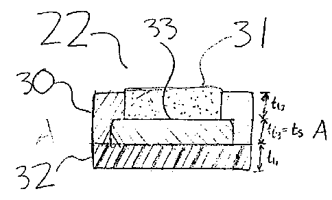
FIGS. 4a and 4b illustrate an embodiment of an insulated strain gage 23
according to the
invention. FIG. 4b illustrates a cross-sectional side view of Fig 4 along line
a-a of FIG. 4a.
Insulated strain gage 23 includes the insulated strain gage 22 with the
addition of another insulating
layer 30 of insulating material and contact pads 31 of conducting material. As
can be seen in FIGS.
4a and 4b, insulating layer 30 is adjacent to the sides and the top of
semiconductive layer 33.
Further, contact pads 31 extend from the top side of insulating layer 30 to a
bottom side of insulating
layer 30 where contact pads 31 contact semiconductive layer 33.
In the embodiment of FIG. 4, insulating layer 30 comprises Si02, which is the
same material
as insulating layer 32, but other insulating materials known by those skilled
in the art to have the
2o same or similar physical and insulating properties adequate for use in an
insulated strain gage 23
may be used. Also, in the embodiment of FIG. 4, insulating layer 32 has both a
top side thickness
tl2 and lateral side thickness t~3 of approximately 2.0 ,um. Thus, in the
embodiment of FIG. 4, the
thickness of the insulated strain gage 23 is the combined thickness of
insulating layer 32,
semiconductive layer 33, and insulating layer 30, which is approximately 6.0
Vim.
In the embodiment of FIG. 4, the conducting material of contact pads 31 is
aluminum.
Alternatively, other conducting materials, particularly metals, with suitably
high electrical
conductivity and thermal resistance may be used, as is well known to those of
skill in the art of
semiconductor manufacturing. These contact pads 31 can be used to connect the
insulated strain
gage 23 to an electrical circuit with, for example, wire bonds.
3o The resistance of the insulated strain gage 23 is r = {axlJ/(wxt), where a
is the resistivity of
the senuconductive layer 33, lg is the active length of the semiconductive
layer 33, w is the width
of the semiconductive layer 33, and is is the thickness of the semiconductive
layer 33. The active
CA 02320857 2000-08-18
WO 99/42799 PCT/US99/03489
_g_
length is the length of the semiconductive layer 33 between the contact pads
31. In the embodiment
of FIG. 4, the semiconductive layer 33 has a resistance of 5,000 L~, thickness
is = 2.0 ~cm, and
resistivity a of 0.12L~-cm, where the width w and the active length 18 of the
semiconductive layer
33 can be designed to achieve the resistance of 5000 i~. Of course, the
manufacturing process can
be altered to change any of these parameters to produce an insulated strain
gage having a desired size
and shape as well as desired electrical and mechanical properties.
One aspect of the invention is that conventional semiconductor manufacturing
techniques
can be used to make the insulated strain gage 22 or 23. Specifically,
conventional methods known
to those of skill in the art of semiconductor manufacturing can be used to
form the insulating layers
30 and 32 and the semiconductive layer 33, dope the semiconductive layer 33,
etch 'openings in
insulating layer 30, and fill the openings with conducting material to form
contact pads 31.
The precision of an automated semiconductor fabrication process produces very
even and
precise insulation layers 32 and 30 and semiconductive layer 33 in comparison
to the manual
processes of conventional strain gage manufacturing used to produce the
conventional strain gage
4 and adhesive layer 3. Furthermore, using automated semiconductor fabrication
reduces the cost
of making a strain gage by eliminating conventional manufacturing labor costs
associated with
manually refining a silicon block and extracting individual strain gages from
the block.
FIG. 5 illustrates an embodiment of a portion of a strain gage assembly 20
including the
insulated strain gage 23, or, alternatively, insulated strain gage 22
according to the invention. Strain
2o gage assembly 20 includes a mechanical sensor 2 that is the same or similar
to the mechanical sensor
2 of the conventional strain gage assembly 1 illustrated in FIG. 1. The strain
gage assembly 20 also
includes an adhesive layer 21 of adhesive and the insulated strain gage 23.
The integral insulating
layer 32 of the insulated strain gage 23 produces a strain gage assembly 20
with several advantages
over the conventional strain gage assembly 1 of FIG. 1, as will be discussed
below.
In the strain gage assembly 20, the insulating layer 32 insulates the
insulated strain gage 23
from the mechanical member 2. As discussed above, insulating layer 32 has a
breakdown voltage
of approximately 1000 V. This is an improvement over the breakdown voltage of
500 V of the
adhesive layer 3, which provided insulation for the conventional strain gage
assembly 1.
In the conventional strain gage assembly 1, the adhesive layer 3 insulated the
strain gage 4
3o from the mechanical member 2. According to the invention, however, the
insulating layer 32
insulates the semiconductive layer 33 of the insulated strain gage 23 from the
mechanical member
2. Consequently, the adhesive layer 21 no longer needs to provide insulation.
Therefore, the
CA 02320857 2000-08-18
WO 99/42799 PC'T/US99/03489
_9_
adhesive layer 21 may be chosen solely for its mechanical performance, without
concern for its
insulating properties. Further, the high breakdown voltage of the insulator 32
eliminates the need
to use a filled adhesive to increase the breakdown voltage of the adhesive
layer 21, which, as
discussed above, impaired the bonding properties and consistency of the
adhesive layer 3. Thus, the
chosen adhesive for adhesive layer 21 may be an unfilled adhesive, thereby
improving the bonding
properties of the adhesive layer 21.
Also, because of the high breakdown voltage and even application of the
insulating layer 32,
a pre-coat is no longer needed to prevent electrical shorts and electrical
leaks. Since, as discussed
above, the pre-coat 5 further impairs the mechanical performance of the
adhesive layer 3, eliminating
1o the need for the pre-coat 5 further improves the mechanical performance of
the adhesive layer 21.
Therefore, being able to choose a non-insulating, unfilled adhesive and not
needing a pre-coat
results in an adhesive layer 21 with improved strength over the adhesive layer
3 of the conventional
strain gage assembly 1. In the embodiment of FIG. 5, the adhesive layer 21 has
a shear strength
between 3,000 and 5,000 p.s.i. and has an operating temperature range from
approximately -60 ° F
to 257° F
The ability to use a non-insulating, unfilled adhesive substantially reduces
the thickness of
the adhesive layer 21. In the embodiment of FIG. 5, the adhesive layer 21 has
a thickness of
approximately 6.0 ~cm, as opposed to a thickness of approximately 25.4 ~,m for
the adhesive layer
3 of the conventional strain gage assembly 1. Also in the preferred embodiment
of FIG. 5, the
insulated semiconductor strain gage 22 or 23 has a thickness of approximately
4.0 ,um or 6.0 Vim,
respectively. Thus, the combined thickness of the insulated strain gage 22 or
23 and the adhesive
layer 21 of approximately 10.0 ,um or approximately 12.0 ~cm, respectively,
represents over a 66%
reduction from the combined thickness of the conventional strain gage 4 and
adhesive layer 3 of 38.1
,um. This reduced thickness results in an improved mechanical performance of
the strain gage
assembly 20.
The insulated strain gage 22 or 23 can be used as a part of variety of devices
known to those
of skill in the art, such as force cells, loads cells, pressure transducers
and accelerometers.
Combinations of insulated strain gages 22 and 23 can be used in combination
with electrical circuitry
to measure forces acting on a mechanical device.
FIGS. 6a and 6b illustrate an embodiment of a pair of insulated strain gages
41 and 42 being
used in combination with a mechanical sensor or beam 40. The strain gages 41
and 42 each may be
either insulated semiconductor strain gage 22 or 23. FIG. 6a shows the
combination at rest. FIG.
CA 02320857 2000-08-18
WO 99/42799 PG"T/US99103489
- 10
6b shows a force F applied to beam 40. Force F causes beam 40 to bend causing
a strain on beam
40. This bend causes strain gage 42 to stretch or be in tension, and causes
strain gage 4 i to compress
or be in compression. For this reason, strain gage 41 is called the
compression gage and strain gage
42 is called the tension gage.
In the embodiment of FIG. 6, two wire bounds 41 A and 41 B are each connected
to an end
of compression gage 41, and two wire bounds 42A and 42B are each connected to
an end of tension
gage 42. If the insulated strain gage 41 or 42 is of the embodiment of
insulated strain gage 23, the
wire bounds connect to contact pads 43. The signals on the wire bounds
indicate the change in
resistance across each strain gage. In FIG. 6, the resistance across
compression gage 41 will
1o decrease and the resistance across tension gage 42 will increase. These
wire bounds can be a part
of the circuitry for calculating the strain on beam 40 as a function of the
change in resistance.
FIG. 7 illustrates one example of such circuitry that includes a Wheatstone
Bridge
configuration 50. Wheatstone bridges are ideal for accurately measuring small
changes in resistance.
In the first embodiment, strain gage 4I and 42 are connected in series with
respect to an input
potential Vi and in parallel with respect to an output potential Vo. An
excitation signal produces an
input voltage Vi of the order of several volts. This configuration could be
part of a pressure
transducer or other such mechanical-electrical translating devices.
As discussed above in the embodiment of FIG. 4, the resistance of the
insulated strain gage
23, or, alternatively, the insulated strain gage 22, is approximately 5,000
fZ. Thus, the resistance of
2o each of the strain gages 41 and 42 is approximately 5,000 Ll. With such a
high impedance and an
input potential of several volts, the resulting output potential Vo will be of
the order of millivolts.
In the embodiment of FIG. 7, amplification circuitry 51 is coupled to the
output signal Vo to produce
an output potential Va of the desired range.
The use of conventional semiconductor wafer technology makes the insulated
strain gage 23
especially useful within integrated circuits, for example, an application
specific integrated circuit
(ASIC). Accordingly, the circuit of FIG. 7 can be manufactured as an ASIC.
Having thus described at least one illustrative embodiment of the invention,
various
alterations, modifications, and improvements will readily occur to those
skilled in the art. Such
alterations, modifications, and improvements are intended to be within the
spirit and scope of the
3o invention. Accordingly, the foregoing description is by way of example only
and is not intended as
limiting. The invention is limited only as defined in the following claims and
the equivalents
thereto.