Note : Les descriptions sont présentées dans la langue officielle dans laquelle elles ont été soumises.
CA 02322685 2000-08-28
WO 00/42719 PCT/IB99/00706
-1-
APPARATUS AND METHOD
FOR IMPROVED CONNECTIVITY IN WIRELESS OPTICAL
COMMUNICATION SYSTEMS
TECHNICAL FIELD
The present invention is related to an apparatus and a method for receiving an
infrared
signal. More particularly, the invention relates to a scheme for selection of
the most
suitable signal.
BACKGROUND OF THE INVENTION
Many devices and most mobile computers today are equipped with wireless
infrared
facilities for communication links. Traditionally, infrared links have been
classified
according to whether they employ a directional or non-directional receiver and
transmitter, and whether or not they rely upon the existence of an
uninterrupted
line-of sight path between the receiver and the transmitter. At present,
directed,
line-of sight Iinks, hereinafter abbreviated to LOS, are the most widely used.
Because
they employ directional receivers and transmitters, the path loss is
minimized, and
multipath distortion is usually negligible. Another link design is the non-
directed,
non-LOS link, also referred to as a diffuse link, which relies upon diffuse
reflection of
light from an extended surface, such as a ceiling and walls.
A unit which is able to transnut and receive infrared signals is called a
transceiver.
Practical wireless infrared transceivers are restricted to use one optical
receiver, which
might be a photodiode {PD) and one optical emitter, which might be a light
emitting
diode (LED). The current types of transceivers based on LOS propagation are
best
suited for point-to-point communication and are not suited for integration in
a mobile or
fixed platform meant to operate in a wireless infrared networking environment.
These
transceivers commonly contain only one optical receiving element that has a
fundamentally different reception characteristic compared to the optical
transmitter's
CA 02322685 2003-12-19
SZ 9-98-022
-2-
characteristic. Such transceivers violate the optical parity rule. Because,
the receiver
exhibits a reception angle spa of about ~60°, also referred to as wide-
angle, and the
transmitter comprises an emission angle ~ of about ~15°, also referred
to as
narrow-angle. This leads to both insufficient connectivity coverage and link
performance degradation in a typical networking application. Insufficient
connectivity
coverage means that i) network participants cannot connect to certain other
participants, ii) certain links are unreliable, or iii) some links offer not
enough
bandwidth for the application, which means that the required data rate can not
be
achieved. Further, the data throughput is low because of the low data rate
and/or high
error rate which means that performance degradation occurs because of reduced
link
quality combined with improper operation of a collision avoidance mechanism.
The optical parity concept was disclosed in the contribution "Request for
Comments on
Advanced Infrared (AIr) IrPHY Physical Layer Specifications", Standards
contribution
to Infrared Data Association (IrDA), Toronto, Canada, April 15-17, 1997,
Version 0.1
(Hewlett-Packard Company and IBM Corporation).
An US Patent No.6,377,376 issued on April 23, 2002 and entitled
"Optoelectronic
Transceiver", discloses a concept of optical transceiver parity. This US
patent
application is presently assigned to the assignee of the instant application.
US Patent No. 5,566,022 is related to an infrared communication system. The
system
includes a plurality of infrared transceivers for receiving and transmitting
infrared
signals through the free air. A circuit determines the direction of arrival of
the received
signal and provides this information to a dedicated logic controller (DLC),
for
registration purposes and for controlling the respective infrared transmitter.
One of the important features of infrared communications is its sensitivity to
the
direction of reception. The publication "Direction Diversity for Indoor
Infrared
Wireless Communication Receivers" by M. R. Pakravan and M. Kavehrad of the
IEEE
International Conference on Communication, June 18-22, 1995, Seattle,
discusses the
CA 02322685 2000-08-28
WO 00/42719 PCT/IB99/00706
-3-
effects of rotation on the characteristics of the received signal from a
simulation point of
view.
The article "Design Considerations for Broadband Indoor Infrared Wireless
Communication Systems" by M. R. Pakravan and M. Kavehard in International
Journal
of Wireless Information Networks, Vol. 2, No. 4, 1995, . is similar to the
publication
mentioned above and discusses the effects of receiver direction and field-of
view on the
channel parameters.
In the paper "Wireless Infrared Communication Links using Multi-Beam
Transmitters
and Imaging Receivers" by A. P. Tang, J. M. Kahn, Keang-Po Ho, of the IEEE
International Conference on Communication, June 23-27, 1996, Dallas, the use
of
imaging receivers in infrared links is analyzed.
The research report "Angle Diversity for Nondirected Wireless Infrared
Communication" by J. B. Carruthers and J. M. Kahn, University of California,
Berkeley,
submitted to IEEE Transactions on Communications, discusses practical
considerations
for mufti-element angle-diversity systems. Unfortunately, the report does not
offer a
practical solution to the present problem because it is based on highly
complex and
costly optical receiver arrays combined with analog high-order signal
selectionlconcentration schemes.
The article "Angle Diversity to Combat the Ambient Noise in Indoor optical
Wireless
Communication Systems" by R. T. Valadas, A. R. Tavares, A. M. de Oliveira
Duarte, in
International Journal of Wireless Information Networks, Vol. 4, No. 4, 1997,
describes
theoretical approaches to estimate several signal-to-noise ratios based on the
analog
current of several photodiodes.
In the article "Signal Processing of High Speed Nondirective Infrared Wireless
Communications" by Po-An Sung, Ya-Ku Sun, Kwang-Cheng Chen, in Journal of the
Chinese Institute of Electrical Engineering, Vol. 2, No. 4, 1995, theoretical
and
numerical results of different diversity techniques are demonstrated.
CA 02322685 2000-08-28
WO 00/42719 PCT/IB99/00706
-4-
All mentioned documents describe several theoretical approaches and
simulations but
these give no practical solution for known technical problems.
Further, network connectivity coverage between mobile platforms, e.g. laptop
computers, and fixed access points, e.g. repeater stations or printers, that
are all
equipped with conventional wireless infrared transceivers is expected to be
insufficient
for typical user scenarios. Usually, one single transceiver is used in mobile
or certain
fixed platforms which leads to the above mentioned problems and disadvantages
in
wireless optical networking application. Some platforms, e.g. laptop
computers, are
equipped with two transceivers and the user has to decide by manual
interventions
which one of the two transceivers is to be used. Thus, current infrared
transceivers are
limited for the use of future wireless infrared applications based on multi-
point
connectivity.
OBJECT OF THE INVENTION
It is an object of the present invention to provide a method and apparatus for
receiving
IS an infrared signal and for selecting the best suited signal from several
received infrared
signals.
It is another object of the invention to overcome the disadvantages of the
prior art.
It is still another object of the present invention to achieve an improved
connectivity in
wireless optical networks.
It is yet another object of the present invention to provide a simple and fast
optical
receiver for reliable reception of an infrared signal.
It is a further object of the present invention to present an apparatus for
receiving or for
receiving and transmitting an infrared signal which provides a sufficient or
even better
connectivity coverage than so-far known arrangements do, i.e. each network
participant
connects with all others with sufficient bandwidth.
CA 02322685 2000-08-28
WO 00/42719 PCTIIB99/00706
-5-
It is still a further object of the present invention to provide a method for
receiving or
for receiving and transmitting an infrared signal in order to achieve reliable
communication links.
SUMMARY AND ADVANTAGES OF THE INVENTION
S The present invention provides an apparatus and a method for improved
connectivity in
wireless optical networks and is particularly suited for mufti-point
connectivity. The
idea is to use at least two or more receiving units which receive an infrared
signal and
convert it to a digital signal. The digital signals represent data in the form
of frames
whereby each frame comprises at least a data field and a header field
containing a
preamble. The preamble is identical for each received signal since it can be
assumed that
each received signal comes from the same source, i.e. from the same
transmitter. A
selector determines a measure related to the signal-to-noise ratio of the
preamble and
compares the measures in order to select the best suited signal for further
processing.
Thus, the selector indirectly estimates a corresponding measure of the signal-
to-noise
ratio of the preamble or from at least a part of the preamble. Thereby it does
not matter
from which direction exactly a signal comes from, rather the best suited
signal is
required. The best or the best suited signal, is to be considered as the
signal with the
lowest error rate or with the highest signal-to-noise ratio, which indicates
that the signal
is least influenced by noise or other distortions. It should be noted, that
the best signal is
not necessarily the strongest signal. It should be noted further, that not the
full or entire
preamble has to be used or investigated to determine the best suited signal.
This
depends on the quality of the received signal and the efficiency of
recognition or
analysis schemes implemented in the hardware.
The present invention provides improved connectivity in wireless optical
networks and
is particularly suited for mufti-point connectivity between mobile platforms
or portable
devices, e.g. laptop computers, hand-held devices, and fixed access points,
e.g. repeater
CA 02322685 2000-08-28
WO 00/42719 PCT/IB99/00706
-6-
stations, printers, or peripheral equipment. A typical user scenario can be a
round-table
configuration comprising a plurality of stations in a conference room
The present invention has the advantage that it requires only simple optical
receivers in
combination with processing of binary signals obtained from at least two or
more
receiving units. A simple converter converts a received infrared signal to a
digital signal,
whereby the digital signals represent data carried in frames comprising at
least a data
field and a header field which contains preamble being identical for each of
the digital
signals. It is a another advantage of the present invention that from several
received
infrared signals the best suited one can be selected fast by a selector and
used for further
processing since the preamble is identical for each signal. It is a further
advantage that
communicating devices equipped with an apparatus according to the present
invention
or a receiving unit and a transmitting unit will not need an alignment as
accurate as
before and are well suited for mufti-point networking applications.
When a preamble of a frame comprises symbols forming a known periodic sequence
of
pulses, preferably a sequence of pulses with defined period, then the
advantage occurs
that predefined symbol sequences can be expected by a digital reception-unit
or a digital
processing-unit and that this unit is able to perform efficient carrier
sensing, symbol
clock synchronization, and chip clock phase acquisition by a phase-locked
loop, also
referred to as PLL.
If the received infrared signal in each receiving unit is converted by a
binary
decision-unit to a digital signal, then the advantage occurs that the further
signal
processing can be performed by digital processing. The received infrared
signal can be
converted by a simple binary decision device, which can be easily implemented.
A huge
advantage, in comparison to a weak analog signal that cannot be forwarded over
long
distances, is that the converted digital signal can be sent over long wires to
a selector or
other processing unit without additional noise penalty. Further, only one
selector is
necessary which can be arranged in a suitable or central place. Analog signals
transmitted over wires are susceptible to interference and suffer from noise
pick-up.
Especially in computer or laptop environments where CD-ROM drives and other
CA 02322685 2000-08-28
WO 00!42719 PCT/IB99100706
equipment create background noise, noise pulses or parasitic frequencies,
digital
processing achieves higher robustness and reliability in practice.
When the digital signal of the preamble is oversampled and weighted, then the
advantage occurs that an efficient method can be applied to estimate the
signal-to-noise
ratio, hereinafter abbreviated to SNR, that exists on each of the two or more
receiving
paths or channels. There is no need to actually erasure the SNR, only the
relative
quality of the different receiving paths is required to select the best
received digital
signal.
If the selection of the one or best suited digital signal occurs during the
reception of the
preamble at the selector, then the advantage occurs that a fast selection of
the one
receiver for further receiving can be performed. The best suited signal can be
received
by one receiver, whereby the other receivers may be switched off to conserve
energy.
When each receiving unit is designed to provide an optical reception
characteristic
which is described by an obtuse reception angle tpR, wherein the reception
angle ~ is a
planar angle that defines where the receiver's sensitivity is half the
sensitivity of the
sensitivity on the receiver's optical axis, then the advantage occurs that a
large
total-reception angle can be provided. This reception angle may cover a range
of about
120°.
If the data are encoded by a pulse modulation, preferably a Pulse Position
Modulation
(PPM), then the advantage occurs that the data can be transmitted in the
baseband and
therefore no complex modulation techniques are necessary.
When at least the receiving unit which receives the preamble with a lower
signal-to-noise ratio than the one receiving unit which receives the one
preamble with
the highest signal-to-noise ratio is switched off, then the advantage occurs
that the
electrical power of the entire circuits and the device can be decreased, which
is
particularly advantageous for mobile devices.
CA 02322685 2000-08-28
WO 00/42719 PCT/IB99/00~06
_g_
If the transmitting unit has an optical reception characteristic whose shape
is identical to
the shape of an optical reception characteristic of the receiving unit, for
example, in the
form of a lrambertian characteristic of ~ ~ ~, whereby the emission angle tpE
is a
planar angle that defines where the power emitted by the transmitter is half
the power of
the power on the transmitter's optical axis, then the advantage occurs that
the optical
parity mle with the desired Lambertian characteristic can be satisfied which
leads to an
improved connectivity coverage. Furthermore, the use of equal Lambertian
reception/emission characteristics in both planes introduce a diffuse-mode
component
that helps to extend connectivity coverage.
When at least one transmitting unit and at least one receiving unit and the
converter are
part of a transceiver or if at least one receiving unit and the converter are
part of an
optical device, then the advantage occurs that all optical components and the
converter
can be integrated to a single transceiver package or optical device package,
which may
save space through integration and energy consumption through combination and
reduce costs for manufacturing and replacements.
If at least three transceivers or several transceivers are arranged to
complement their
optical reception characteristics and/or optical emission characteristics,
then the
advantage occurs that full coverage for connectivity over a range of
360° can be
achieved.
When a selector is connected to a unit comprising at least a first modem unit
and/or a
second modem unit, then the advantage occurs that the selector can operate
with units
providing several rates and/or speeds, e.g. for variable rate, fixed rate,
high speed, low
speed.
If the selector is combinable with at least one modem unit, preferably with
the fast
modem unit, then the advantage occurs that the selector and the modem unit can
be
implemented in a single unit or chip. This unit or chip can be implemented
easily in
current systems to improve their connectivity according to the present
invention.
CA 02322685 2000-08-28
WO 00!42719 PCT/IB99/00706
_g_
When at least the seiector, the first modem unit, and the second modem unit
are
combinable to a single unit, then the advantage occurs that space through
integration
can be saved and that the functions of the units and the selector are
implemented in a
single unit or chip. _
Given that the objective of improved connectivity should be met with current
or,
preferably, simply improved transceivers, the need arises to equip a platform,
i.e. laptop
computers, LAN access points, repeater stations, printers, hand-held devices,
or other
devices, with more than one wireless infrared transceiver. This calls for an
apparatus
andlor a method for the interconnection and control of several transceivers to
achieve a
required angle diversity by appropriately combining or selecting the
respective signals of
the different transceivers.
CA 02322685 2000-08-28
WO 00/42719 PCTIIB99/00706
- 10 -.
DESCRIPTION OF THE DRAWINGS
The invention is described in detail below with reference to the following
schematic
drawings.
FIG.1 shows a schematic illustration of an arrangement according to the
present invention with three transceivers, the accompanying signals, and
a selector.
FIG. 2 shows a schematic illustration of a comparator and some sampling- and
counting units.
FIG. 3 shows some steps of an analysis of an oversampled bit sequence.
FIG. 4 shows a basic internal architecture of a selector.
FIG S shows a basic embodiment of an infrared communication system with
three-fold channel diversity according to the present invention.
FIG. 6 shows a further basic embodiment of an infrared communication system
with three-fold channel diversity.
All the figures are for the sake of clarity not shown in real dimensions, nor
are the
relations between the dimensions shown in a realistic scale.
CA 02322685 2000-08-28
WO 00/42719 PCT/IB99/00706
-11-
DETAILED DESCRIPTION OF THE INVENTION
Before embodiments of the present invention are described, some basics, in
accordance
with the present invention, are addressed.
PPM - Pulse Position Modulation:
A Pulse Position Modulation sche~, hereinafter abbreviated to PPM, is used in
accordance with the present invention. It should be noted, that other
modulations
schemes can be used instead, especially advantageous are pulse modulations,
e.g.
Run-Length Limited Codes, also abbreviated to RLL. The PPM provides a variable
data
rate with repetition coding. L-slot Pulse Position Modulation is achieved by
defining a
data symbol of duration tp and subsequently subdividing the symbol into a set
of L, e.g.
L= 2, 4, 8, 16, equal time slots, also called 'chips'. In L-PPM schemes, only
one time
slot, or chip, per symbol contains a pulse, which means a logical 'one' or
'1'. The other
chips contain no pulse, which means a logical 'zero' or '0'. If the base is
defined as
L=4, then the resulting modulation scheme is called four Pulse Position
Modulation or
1S 4-PPM. Because there are four unique positions within each 4-PPM symbol,
four
independent symbols exist in which only one chip is logically '1' while all
other chips
are logically '0', whereby there are the following combinations: 1000, 0100,
0010,
0001. These four symbols are the only legal data symbols allowed in 4-PPM.
Each data
symbol represents two bits of a single data bit pair, which are respectively
00, O1, 10,
11. Logical '1' represents a chip duration when a transmitter is emitting
light, while
logical '0' represents a chip duration with no light emission.
The preamble:
A digital signal according to the present invention represents data carried in
frames,
whereby each frame comprises at least a data field and a header field which
contains a
preamble. The preamble comprises a periodic symbol sequence to allow for
initial
carrier sensing, symbol clock synchronization, and chip clock phase
acquisition by a
phase-locked loop, also referred to as PLL. This means in particular that the
preamble is
CA 02322685 2000-08-28
WO 00142719 PCT/IB99/00706
- 12-
employed to obtain initial relative synchronization of a digital reception-
and
processing-unit, which is achieved by the transmission of a periodic sequence
of pulses.
A receiving station which knows how many slots each symbol comprises, is able
to
detect after a certain while the period of the sequence of pulses.
Furthermore, the_
receiving station adjusts its slot or chip clock phase using a PLL. The
preamble
comprises a plurality of repeated transmissions, prefer=ably 128 or more, of
the
following legal 4-PPM symbol P: P = 1000. Every other combination is possible
if it is
use- or helpful, e.g. for additional information transmission. After the
preamble may
follow a synchronization field, a control field, the data field or other
fields.
The optical parity:
Unlike radio systems, infrared systems use two physically different elements
for
reception and transmission which can be a photodiode (PD) and a light emitting
diode
(LED). Since the reception characteristic of a receiver is different from the
emission
characteristic of a corresponding transmitter, shortcomings occur not only
with data
rates. The establishment of transmission symmetry or transceiver parity allows
symmetrical data rates, maintains collision avoidance properties, and improves
connectivity.
A receiving unit according to the present invention comprises at least a
receiver and an
analog-to-digital converter. The receiver has an optical reception
characteristic
described by a reception angle ~, also referred to as the receiver's half
angle ~.
Similarly, a transmitter has an optical emission characteristic described by
an emission
angle ~, also referred to as the transmitter's half angle ~. A transceiver is
characterized in that it comprises at least an optical emitter element and an
optical
receiver element, whereby a transmitter is not restricted to one single light
emitting
element and a receiver is not restricted to one single light receiving
element. The optical
transmitter is constructed such that its three-dimensional emission
characteristic is
identical or at least similar to the three-dimensional optical reception
characteristic of
the receiver. The use of optical parity or transceiver parity allows
coexistence of
CA 02322685 2003-12-19
SZ 9-98-022
-13-
devices with different optical ports supporting narrow- or wide angle as well
as short
range or longer range transmission. Details of the concept are addressed and
claimed in
the US patent no.6,377,376 issued on April 23, 2002 and entitled
"Optoelectronic
Transceiver".
In the following, embodiments of the invention are described.
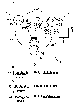
FIG. 1 shows an apparatus 4 for receiving and/or transmitting an infrared
signal in a
wireless optical communication system or in a wireless optical network. A
first
transceiver 13, a second transceiver 23, and a third transceiver 33 are
arranged in a
staggered manner. The angle between the optical axis of adjacent transceivers
13, 23,
33 is about 120°, whereby the basic geometrical arrangement of the
three transceivers
13, 23, 33 can achieve 360° of horizontal angular coverage at an
optical interface of a
mobile or fixed platform equipped for wireless optical networking. The fully
integrated
first transceiver 13 for a first channel comprises a first receiving unit 1
including a
receiver which is here a photodiode revealing a Lambertian first reception
characteristic 14 and reception circuitry. Further, a first transmitting unit
11 comprises
at least one transmitter which here is a light emitting diode, called an
emitter, a diffuser
above the transmitter revealing a Lambertian first emission characteristic 15,
and
transmission circuitry. The diffuser is further described below.
It should be noted, that the emission characteristic 15, 25, 35 of the radiant
intensity in
units of mW/sr follows, or at least approximately, the cosine law, which is
cos(~p)"',
m = 1. The reception characteristic 14, 24, 34 of the optical receiver follows
the same
law.
The reception- and transmission circuitry is combined with a converter in a
first
transceiver chip 12, but nevertheless the first transceiver chip 12 can be
separated in
two or more single chips if that is advantageous. The components are mounted
on a
common lead frame and molded in a plastic package. The first transceiver chip
12 of
the first transceiver 13 has a connection to a selector 5. The structure of
the two other
CA 02322685 2000-08-28
WO 00/42719 PCT/IB99/00706
- 14-
transceivers 23, 33 is equivalent. Therefore, the second transceiver 23 for a
second
channel comprises a second receiving unit 2, a second transmitting unit 21,
and a
second transceiver chip 22. The second transceiver chip 22 of the second
transceiver 23
is connected to the selector S. The third transceiver 33 for a third channel
comprises a
third receiving unit 3, a third transmitting unit 31, and a third transceiver
chip 32. The
third transceiver chip 32 of the third transceiver 33 is connected to the
selector 5. Each
transceiver 13, 23, 33 comprises a characteristic, whereby the first reception
characteristic 14 and the first transmission characteristic 15, which are
similar to each
other, are schematically depicted in front of the first transceiver 13. A
second reception
characteristic 24 and a second transmission characteristic 25 are
schematically depicted
in front of the second transceiver 23. Further, a third reception
characteristic 34 and a
third transmission characteristic 35 are schematically depicted in front of
the third
transceiver 33. A first arrow in the direction of the first transceiver 13,
labeled with S 1,
indicates a part of an arriving first infrared signal S 1. For the sake of
clarity, this first
1 S infrared signal S 1 with an ideally infinite signal-to-noise ratio is
depicted as S 1 below
the transceiver arrangement. A second arrow in the direction of the second
transceiver
23, labeled with S2, indicates a part of an arriving second infrared signal
S2, which
arrives during the same time. The second infrared signal S2 with a signal-to-
noise ratio
of about 20 dB is also depicted below the transceiver arrangement of the
apparatus 4.
Furthermore, a third arrow in the direction of the third transceiver 33,
labeled with S3,
indicates a part of an arriving third infrared signal S3, which arrives also
during the
same tip. The third infrared signal S3 with a signal-to-noise ratio of about S
dB is also
depicted below the transceiver arrangement.
The above mentioned diffuser is constructed in front of each transmitting unit
11, 21,
31 such that it provides a 60° half power angle in all planes
comprising the optical
emission characteristics 1 S, 25, 35. The diffuser can be constructed, for
example, from
plastic material or other materials with embedded glass beads to achieve
different
indexes of refraction within the diffuser. Besides the advantages for improved
connectivity, the diffuser offers additional advantages with respect to
compliance with
the eye safety norm IEC 825.1 because the apparent source size is determined
by the
CA 02322685 2003-12-19
SZ 9-98-022
-15-
diffuser size, rather than the transmitter chip size. The diffuser approach
offers a
simpler lead frame structure than alternative approaches where several
conventional
narrow-angle emitters are combined to achieve wide-angle emission. In cases
where
increased radiant intensity is required it is possible to mount several
optical emitters
underneath a common diffuser. Details of suited diffusers are given in the PCT
international application with the International Publication Number WO
96/08090. This
PCT application is presently assigned to the assignee of the instant
application.
In FIG. l, the first infrared signal S 1 is being received by the first
transceiver 13, the
second infrared signal S2 is being received by the second transceiver 23 and
the third
infrared signal S3 is being received by the third transceiver 33. Each
received signal S 1,
S2, S3 is converted to a digital signal, i.e. the first infrared signal S1 is
converted to a
first digital signal RxS_1, the second infrared signal S2 is converted to a
second digital
signal RxS_2, the third infrared signal S3 is converted to a third digital
signal RxS_3.
For the sake of clarity, the first digital signal RxS_1, the second digital
signal RxS 2,
and the third digital signal RxS_3 are depicted below the transceiver
arrangement,
respectively. In the following, the conversion is described as an example with
the first
infrared signal S 1 on the first transceiver 13 but it is the same principle
for the other
two infrared signals S2 and S3 and its transceivers 23, 33, respectively. The
conversion
of the first infrared signal S 1 takes place on the first transceiver chip 12.
The first
transceiver chip 12 is situated very close to the first receiver unit 1 in
order to avoid
long leads or wires which can be influenced by noise. First, the received
first infrared
signal S 1 is guided to the first transceiver chip 12 and amplified by an
amplifier before
it is fed to a variable gain amplifier. The variable gain amplifier controlled
by automatic
gain control circuitry assures that the signal level at the following decision
device is
kept constant over the specified range of received optical signal power. The
mentioned
decision device is a binary decision-unit or a threshold value switch, also
referred to as
threshold decision device or comparator, which converts the first infrared
signal S 1 to
the first digital signal RxS-1 by comparing the first infrared signal S 1 to a
threshold.
This first digital signal RxS_l, as depicted below the apparatus 4, is fed to
the
CA 02322685 2000-08-28
WO 00142719 PCT/IB99/00706
- 16-
selector 5. The say is performed with the second infrared signal S2 and the
thud
infrared signal S3, respectively. The second infrared signal S2 is converted
to the
second digital signal RxS_2 and fed to the selector S. The third infrared
signal S3 is
converted to the third digital signal RxS 3 and also fed to the selector 5.
Thus, the
three transceivers 13, 23, 33 are connected to the selector 5 providing
functions for
channel combining, selection and control. Depending 'on the control mechanism
implemented in selector 5, a three-fold channel diversity can be exploited to
obtain
different modes of angle diversity for network connectivity. The selector 5
determines
the best suited signal for further processing and passes on this best suited
signal to
further units via an output line xy. The method used to determine the best
suited signal
is described in detail with reference to FIG. 2 and FIG. 3. The apparatus 4 is
able to
receive and transmit data which is indicated by arrows in both directions on
first, second
and third signal lines to and from the selector 5, labeled with RxS_1, RxS 2,
and
RxS_3, respectively, which here indicates the received signals and labeled
with TxS_ 1,
IS TxS_2, and TxS 3, respectively, which here indicates the transmitted
signals of
transmit-data.
FIG. 2 shows a schematic illustration of elements and units which together are
able to
determine the best suited signal from different signals for further
processing. For a first
channel a first binary decision-unit 12.1 is connected to a first sampling-
and counting
unit 16. This first sampling- and counting unit 16 includes a first sampler
17, a first
serial shift register 17.1, a first array of independent sample-counters 18,
hereinafter
referred to as first sample-counters 18, and a first total-counter 19. The
first sampler 17
is connected to the first serial shift register 17.1 which further is
connected to the first
sample-counters 18. The first sample-counters 18 are connected to the first
total-counter 19. For a second channel a second sampling- and counting unit 26
is
arranged. This second sampling- and counting unit 26 includes a second sampler
27, a
second serial shift register 27.1, a second array of independent sample-
counters 28,
hereinafter referred to as second sample-counters 28, and a second total-
counter 29.
The second sampler 27 is connected to the second serial shift register 27.1
which
further is connected to the second sample-counters 28. The second sample-
counters 28
CA 02322685 2000-08-28
WO 00/42719 PCT/IB99100706
- 17-
are connected to the second total-counter 29. For a third channel a third
sampling- and
counting unit 36 is arranged. This third sampling- and counting unit 36
includes a third
sampler 37, a third serial shift register 37.1, a third array of independent
sample-counters 38, hereinafter referred to as third sample-counters 38, and a
third
total-counter 39. The third sampler 37 is connected to the third serial shift
register 37.1
which further is connected to the third sample-counters 38. The third
sample-counters 38 are connected to the third total-counter 39. Further, the
first
sampling- and counting unit 16 is connected to a first number-memory 7, the
second
sampling- and counting unit 26 is connected to a second number-memory 8, and
the
third sampling- and counting unit 36 is connected to a third number-memory 9.
All
number-memories 7, 8, 9 are connected to a comparator 6, also referred to as
selector
or number-comparator 6. The number-memories 7, 8, 9 can also be included in
the
sampling- and counting units 16, 26, 36, respectively.
The first binary decision-unit 12.1 comprising a first input 'a' for the
received first
infrared signal S 1 and a second input 'b' for a threshold 'TH'. This first
binary
decision-unit 12.1 is positioned on the described first transceiver chip 12,
as mentioned
with reference to FIG. 1. For the sake of simplification only one binary
decision-unit is
depicted in FIG. 2 whereas for each channel such a binary decision-unit is
used. The
first binary decision-unit 12.1 compares the first infrared signal S 1 with
the threshold
'TH' and puts out a first digital signal RxS_1 which is fed to the first
sampler 17 of the
first sampling- and counting unit 16. If the value of the first infrared
signal S 1 is larger
than the value of the threshold 'TH', that means S 1 > TH, a logic level ' 1'
is generated
at the output of the first binary decision-unit 12.1, otherwise a logic level
'0' is
generated. A second digital signal RxS_2 coming from the second transceiver
chip 22,
shown in FIG. 1, and generated by a second binary decision-unit, is fed to the
second
sampler 27 of the second sampling- and counting unit 26. A third digital
signal RxS 3
coming from the third transceiver chip 32, also shown in FIG. l, and generated
by a
third binary decision-unit, is fed to the third sampler 37 of the third
sampling- and
counting unit 36.
CA 02322685 2000-08-28
WO 00/42719 PCT/IB99/00706
- 18-
The principle process used to determine a erasure, a number, or a value in
order to
select the best suited signal is described with reference to the first
sampling- and
counting units 16 in more detail in connection with FIG. 3. The process is
repeated until
a rr~asure or a value of a given or definite threshold is reached. However,
the
S two sampling- and counting units 26 and 36 perform in the same way as the
first
counting unit 16 so that the following describes the process for the first
sampling- and
counting unit 16 only. The equivalent length of four slots or chips of a tirr~
interval of
the preamble from the first digital signal RxS_ 1 are fed to the first
sampling- and
counting unit 16. The time interval represents a full 4-PPM symbol but does
not need to
start with a pulse, rather it starts anywhere. In order to accumulate in phase
with
previous time intervals in the sample-counters 18, the subsequent time
intervals should
be equivalent with respect to their time phase. The arriving first digital
signal RxS_1 is
oversampled in the first sampler 17 of the first sampling- and counting unit
16 and put
as binary sequence in the first serial shift register 17.1, whereby here each
chip is
oversampled by four to obtain sixteen binary digits for a defined time
interval. The
binary digits are stored in single-bit registers or flag registers, where the
binary digits
arrive in the form of a sequential row. If sixteen binary digits from the
defined time
interval have arrived in the first serial shift register 17.1, then the first
sample-counters
I8 accumulate to their stored values the binary digits from the respective
single-bit
registers of the first serial shift register 17.1. This process is repeated
for the following
time intervals until the total-counter 19 calculates a first measure 'A' which
is put in the
first number-memory 7. The number of repetitions depends on statistics, the
quality of
the received signals, and the efficiency of recognition or analysis scheme.
The second
sampling- and counting unit 26 determines a second measure 'B' and puts this
measure
in the second number-memory 8. The third sampling- and counting unit 36
determines a
third measure 'C' and puts this measure in the third number-memory 9. The
number-memories 7, 8, 9 are connected to the number-comparator 6 or even
implemented in the number-comparator 6. The number-comparator 6 compares the
cr~easures 'A', 'B', 'C' and determines the best suited signal for further
processing. FIG.
2 indicates that the output of the number-comparator 6 selects the channel
CA 02322685 2000-08-28
WO 00142719 PC'TIIB99/00706
- 19-
corresponding to measure 'A', this is indicated by labeling the output of the
number-comparator 6 with S~. Therefore, from three infrared signals S 1, S2,
S3, the
first infrared signal S1 and thus the first digital signal RxS_l, also
referred to as the one
digital signal RxS_1, is the best suited signal for further processing.
S The above scheme works since it is known and investigated that a relation
exists
between the signal-to-noise ratio and the error rate of a signal. For
instance,
investigations showed that the determined calculated measure, e.g. 'A', is
directly
related to the signal-to-noise ratio of the corresponding signal. This means,
that the
higher the determined calculated measure is, the lower the signal-to-noise
ratio is. Thus
it is su~cient to compare numbers or the r~asures A, B, C and find the
smallest of the
set { A, B, C j to determine the channel or path with the highest signal-to
noise ratio.
Turning now to FIG. 3 which shows some steps of an analysis of an oversampled
binary signal at different times. These steps are performed through the
sampling- and
counting unit 16, shown in FIG. 2. More particularly, FIG. 3 shows the first
serial shift
register 17.1 and the attached first sample-counters 18 at a first time
interval T, and a
second time interval T2, respectively, and further below only the sample-
counters 18 at
a tenth time interval T,o and at a thirty-second time interval T32,
respectively. The first
measure 'A' is calculated after the thirty-second time interval T3z and stored
in the
number-memory 7. The first serial shift register 17.1 comprises sixteen single-
bit
registers which are indicated by single-bit register numbers 1, 2 .... 16
above the first
serial shift register 17.1. These single-bit register numbers and sixteen
single-bit
registers are related to a sample clock 10, shown above a sequence of the
first time
interval T,.
For the sake of clarity, on the top are depicted two time intervals of a noisy
digital
signal of a preamble over a time axis t comprising four pulses, i.e. four
logical 'one' or
'1' having different pulse duration. Within the first time interval T, occurs
only one
pulse whereas in the following second time interval TZ three pulses occur,
whereby two
pulses are error pulse caused by noise. The first time interval T, corresponds
to the
length of a legal 4-PPM symbol. As mentioned above, with the fast time
interval T, four
CA 02322685 2000-08-28
WO 00/42719 PCT/IB99100706
-20-
chips of the preamble from the first digital signal RxS_1 are fed to the
sampler 17,
shown in FIG. 2.
The first time interval T, represents the length of a full symbol but
generally such a time
interval does not need to be aligned with a preamble symbol, rather in this
example it
starts with logical 'zero' instead of a pulse. The reason is that symbol
synchronism and
even chip synchronism has not to been established yet by the receiver. In
fact, the
scheme does not require such synchronism At some time the four oversampled
chips of
the first tithe interval T,, which physically are depicted beside the first
serial shift
register 17.1 and sample-counters 18, are stored in the first serial shift
register 17.1,
whereby each chip is oversampled by four to obtain sixteen binary digits.
Where a pulse
occurs, there results a 'I' otherwise a '0'. The binary digits are stored in a
simple
register comprising single-bit registers or flag registers which can be set or
not. Looking
at the single-bit registers of the first serial shift register 17.1 shows that
the single-bit
registers from the third to the seventh single-bit register result in '1',
whereby one
single-bit register includes a binary digit 30. The individual binary digits
from the
single-bit registers of the first serial shift register 17.1 are accumulated
to corresponding
stored values in the first sample-counters 18. Here, the length of the array
of
sample-counters 18 is identical to the first serial shift register 17.1. For
instance, a
counter value 70, that indicates one stored value, in the first sample-
counters 18 from
the first pulse results in '1' in the first step. This counter value 70 and
its stored value is
observed further in detail. Refer now to the next time interval as depicted
below.
During the second time interval Tz the chips are oversampled and the binary
digits are
put in the first serial shift register 17.1, respectively. By the way, the
former single-bit
registers are overwritten. The result is shown in the row of the first serial
shift register
17.1 at the second time interval Tz. The first sample-counters I8 add the set
single-bit
registers or flags to the former counter values, respectively. After the
addition, the
counter values of the first sample-counters 18 are adapted, e.g. the observed
counter
value 70 has been increased by one and results in "2". Some time later,
indicated by a
dotted vertical line between the second time interval Tz and the tenth time
interval T,o,
which means eight steps further at the tenth time interval T,~, a further
sequence has
CA 02322685 2000-08-28
WO 00/42719 PCT/IB99/00706
-21-
been oversampled. The first sample-counters 18 show the result of the tenth
step. The
observed counter value 70 has been increased and results in "8". Finally, at
the
thirty-second time interval T32, a still further sequence has been
oversampled. The result
is shown in the row of the first sample-counters 18. The observed counter
value 70 has_
been increased and results in "26". The counter values of the first sample-
counters 18
are calculated to a sum of digits to yield a measure 'A''; this is performed
in a not
depicted total-counter. This measure 'A' results in "184" and is stored in the
first
number-memory 7 for further processing as described with reference to FIG. 2.
A further embodiment includes a threshold, preferably at the last step before
the
measure 'A' is calculated, in order to set high numbers, that result from
preamble pulses
and not from noise, return to 'zero'. This is advantageous for better
discrimination and
determination of noise.
FIG. 4 shows an embodiment of a basic internal architecture of a selector 40.
The
selector 40, also referred to as channel combiner, comprises a fast channel-
quality
estimator unit 41 receiving RxS_1 signals, a second channel-quality estimator
unit 42
receiving RxS_2 signals and a second channel-quality estimator unit 43
receiving RxS 3
signals. All channel-quality estimator units 41, 42, 43 are connected to an
evaluation
unit 44 whose output is guided to a control unit 45 and which is able to
receive a
control signal, indicated by the dotted line with an arrow to the control unit
45. The
- control unit 45 is connected on one side to a RxS combiner/selector unit 46.
The RxS
combiner/selector unit 46 is able to receive RxS_1, RxS_2, RxS 2 signals and
to
deliver a RxD_VR signal and a RxD_HR signal. Further, the control unit 45 is
connected on the other side to a TxS enabler/driver unit 47 which delivers a
TxS 1
signal, a TxS 2 signal and a TxS_2 signal. The control unit 45 is also
connected to a
TxD selector unit 48 which is connected to the TxS enabler/driver unit 47. The
TxD
selector unit 48 is able to receive data in form of a TxD_VR signal and a
TxD_HR
signal.
The selector 40 delivers signals, labeled TxS_1, TxS_2, and TxS 3, to
transmitters by
means of the TxS enabler/driver unit 47. For the sake of clarity, the
transmitters are not
CA 02322685 2000-08-28
WO 00!42719 PCT/IB99/00706
-22-
depicted in FIG. 4 but the signals can be fed to the transceivers 13, 23, 33
shown in
FIG. 1, respectively. The TxS enabler/driver unit 47 receives its input signal
from the
TxD selector unit 48 which selects the data to be transmitted from the TxD_VR
signal
and the TxD_HR signal. The TxS enabler/driver unit 47 and the TxD selector
unit 48_
are both controlled by the internal control unit 45. The received signals,
labeled RxS_1,
RxS_2, and RxS 3, are each processed in parallel by the channel-quality
estimator units
41, 42, 43 respectively whose outputs are examined in the evaluation unit 44.
With
reference to FIG. 2 and FIG. 3, the described processes can be implemented in
the
channel-quality estimator units 41, 42, 43 and the evaluation unit 44. The
latter unit
delivers its output to the control unit 45. This control unit 45 also provides
contra! for
the RxS combineriselector unit 46 which processes the RxS_1, RxS_2, RxS_2
signals
and delivers the RxD_VR signals and the RxD_HR signals.
According to another embodiment, the received signals, labeled RxS_1, RxS_2
and
RxS 3, are processed in sequence by a single channel-qua3ity estimator unit
whose
output is examined in the evaluation unit 44.
According to still another embodiment, the RxS combiner/selector unit 46
delivers only
the RxD_VR signal and the TxS enabler/driver unit 47 receives directly the
TxD_VR
signal. Then, no TxD selector unit 48 is required.
According to a further embodiment, the RxS combinerlselector unit 46 delivers
only the
RxD_HR signal and the TxS enabler/driver unit 47 receives directly the TxD_HR
signal. In that case, no TxS selector unit 48 is required.
According to still a further embodiment, the selector 40 provides means for
processing
signals for only two transceivers, whereby then only two-fold channel
diversity is
achievable.
FIG. 5 shows a basic physical layer structure of an embodiment of an infrared
communication system with three-fold channel diversity. Some elements and
units are
the same as used and described above and there referenced with the same
numbering.
CA 02322685 2000-08-28
WO 00!42719 PCT/IB99/00706
-23-
For the sake of simplification of the FIG. 5, the transceivers 12, 23, 33 are
arranged in a
row. However, to achieve three-fold channel diversity it is necessary to
arrange the
transceivers 12, 23, 33 in different or preferred directions. The transceivers
12, 23, 33
are able to receive and transmit infrared signal, which are indicated by
arrows in front o~
the transceivers 12, 23, 33. The transceivers 12, 23, 33 are connected to the
selector 40
that contains the functions that are necessary to provide 'the system with the
desired
angle diversity. The selector 40 is connected to a VR modem/controller 51 and
a HR
modem/controller 61. The VR modem/controller 51, also referred to as second
modem
unit 51 or Variable Rate modemlcontroller 51, has a connection to the
transceivers 12,
23, 33 via a transceiver control line 54 and to a host interface 52. The HR
modem/controller 61, also referred to as first modem unit 61 or High Rate
modem/controller 61, is also connected to the host interface 52 and has, via a
control
line 62, a connection to the selector 40. The host interface 52 is connected
to a host 53.
The transmitted signals, labeled TxS_l, TxS_2 and TxS 3, carry the modulation
signal
IS for the transceivers 12, 23, 33. For example, the TxS_1, TxS 2 and TxS 3
signals are
encoded to 4-slot Pulse Position Modulation (4-PPM), as described above. The
received signals, labeled RxS_l, RxS_2 and RxS 3, carry the signals obtained
from the
respective receiver. As mentioned, in the preferred implementation these
signals are
binary-valued signals. The selector 40 receives data to be transmitted from
either the
VR modem/controller 51 or the HR modem/controller 61. The corresponding data
lines
are labeled TxD_VR and TxD_HR, respectively. Similarly, the selector 40
delivers
received data to the VR rr~dem/controller 51 or the HR modem/controller 61,
whereby
the corresponding data lines are labeled RxD_VR and RxD_HR, respectively. The
VR
modem/controller 51 and the HR modem/controller 61 are able to receive and
transmit
different data rates, e.g. the VR modemlcontroller 51 is able to work with
data rates up
to 4 Mbps and the HR modemlcontroller 61 supports data rates about 16 Mbps.
However, the VR modem/controller 51 controls the operation mode of the
transceivers
12, 23, 33 by issuing commands for setting decision threshold, bandwidth,
transmitter
power level, and others. The HR modem/controller 61 controls the operation
mode of
the selector 40 by issuing relevant commands. These commands include
instructions for
the receiver path on how to combine and/or select the RxS_1, RxS_2 and RxS_3
CA 02322685 2000-08-28
WO 00/42719 PCTIIB99100706
-24-
signals as well as for the transmit path on how to enable the TxS _1, TxS 2
and TxS_3
signals. The VR modem/controlIer 51 and HR nwdem/controIler 61 are connected
to
the host interface 52 by means of a bus, labeled as bus signals VR_IF and
HR_IF,
respectively. The host interface 52 is connected to the host 53 through a bus
line labeled
H_IF for communication with the protocol stack, e.g. medium access control,
also
abbreviated to MAC.
FIG. 6 shows a further basic embodiment of an infrared communication system
with
three-fold channel diversity. All described elements and functions are the
same, with the
difference that the functions implemented in the HR modem/controller 61 and
the
selector 40 are combined in a single selector 40.1.
Regarding to FTG. 5 and FIG. 6, several combinations of elements and units are
feasible. Some are addressed in the following.
According to another embodiment, the selector 40 is arranged as a single unit,
the VR
modem/controller 51 and the HR modemlcontroller 61 are combined in a further
single
I5 unit.
According to another embodiment, the functions implemented in the selector 40,
the
VR modem/controller 51, and the HR modem/controller 61 are all combined in a
single
unit.
According to still another embodiment, the HR modem/controller 61 is not
present and
the selector 40 is controlled from the VR modem/controller 51.
According to a further embodiment, the HR modemlcontroller 61 is not present
and the
selector 40 and the VR modem/controller 51 are both combined in a single unit.
According to still a further embodiment, the VR modem/controller 51 is not
present and
the three transceivers 13, 23, 33 are controlled from the HR modem/controller
61.
CA 02322685 2000-08-28
WO 00/42719 PGT/IB99/00706
-25-
According to yet another embodiment, VR modem/controller 51 is not present and
the
selector 40 and the HR modem/controller 61 are both combined in a single unit.
Any disclosed embodiment may be combined with one or several of the ~ other
embodiments shown and/or described. This is also possible for one or more
features of
the embodiments. The steps herein described and claimed do not need to be
executed in
the given order. The steps can be carried out, at least to a certain extent,
in any other
order.