Note : Les descriptions sont présentées dans la langue officielle dans laquelle elles ont été soumises.
CA 02323259 2000-10-12
~ .
ATOMICALLY SHARP EDGED CUTTING BLADES
AND METHODS FOR MAKING SAME
FIELD OF THE INVENTION
The present invention relates to devices having extremely sharp.cutting
edges, which are particularly useful for surgical instruments, and methods of
making said devices. Indeed, the invention relates to a process for forming an
atomically sharp cutting edge in a- material using single or dual focused ion
beam milling and the devices produced thereby. The invention is particularly
useful in the manufacture of surgical cutting instruments, yet can be used to
provide almost any cutting edge where increased sharpness of the cutting edge
is desirable.
BACKGROUND OF THE INVENTION
Modezn medical procedures require cutting instruments of exceptional
sharpness and wear resistance and which, moreover, exhibit minimal tissue
resistive forces. In delicate microsurgery and especially ophthalmologic
surgery, cutting edges must be extremely sharp and must maintain that
sharpness throughout the operation. However, even presently available acutely
sharpened blades can exhibit substantial resistive forces, making it difficult
to
move through tissue without producing a"ragged" cut. Moreover, studies have
CA 02323259 2000-10-12
~ . ,
. , .
shown that blade degradation can lead to tissue damage, post-operative
complications, and slower healing.
A critical element of a surgical blade is the cutting edge. Chips, nicks or
breaks in the integrity of the edge, residual burrs, and/or rolled or
distorted
cutting edges of the blade can render the blade useless or, even worse, can
injure the patient.
Sharp-edged cutting instruments typically are produced from metals
such as stainless steel, Carborundum, or other relatively hard materials, such
as silicon carbide, silicon, glass, sapphires, rubies or diamonds. Glass,
silicon
and stainless steel are relatively cheap and therefore disposable, while
diamonds, rubies and sapphires are relatively expensive and, of necessity,
typically require reuse as a matter of economics. Each of these materials can
be ground, stamped, etched, lapped or honed by a myriad of means to provide
a cutting edge. For example, metal can be ground, stamped and/or etched to
produce cutting blades with extremely fine cutting edges. However, the thinner
the cutting edge of the metal becomes, the narrower becomes the bevel angle(s)
that forms that cutting edge. As a result, thinner-edge metal cutting blades
exhibit greater fragility than relatively thicker edged blades. This fragility
manifests by significant wear, i.e., chips, nicks, breaks, residual burrs,
and/or
rolled or distorted cutting edges. Moreover, metal cutting blades can dull
significantly even during a single use.
2
CA 02323259 2000-10-12
Many of those skilled in the art have considered a diamond blade as the
accepted standard for sharpness. However, diamond blades are very
expensive, extremely delicate, and still require resharpening on a regular
basis.
Thus, those sldlled in the art have sought, by a variety of means, more
economical means of fashioning cutting devices with diamond-like sharpness.
Some of the more recent attempts to provide hard sharp cutting edges are
discussed below.
Henderson (US 4,534,827) discloses a cutting instrument fabricated by
etching and chemically polishing a single crystal of aluminum oxide material,
e.g., rubies or sapphires, to form an edge having a maximum radius of
curvature of about 100 Angstroms (A). However, the disclosed materials are
brittle and, moreover, the cutting blades formed by the lattice of the
material
exhibit a natural bevel incline.
Mirtich et al. (US 4,490,229) discloses a method for maldng diamond like
carbon films on a substrate. The surface of the substrate is exposed to an
argon ion beam that contains hydrocarbon. At the same time, a second argon
ion beam (without hydrocarbon) having greater ion energy is directed toward
the surface, which increases mobility of the condensing atoms and removes
lesser bound atoms.
Bache et al. (US 4,933,058) discloses a method for coating a cutting
substrate with a harder material by chemical vapor deposition or sputtering,
while simultaneously subjecting the cutting edge to ion bombardment. Ion
3
CA 02323259 2000-10-12
t. =
bombardment causes preferred depositional orientation of the harder material
and, moreover, causes sputter removal of the deposited material, which
produces a coating with a particular cross-sectional shape and ultimate tip
radius.
Kokai (Japanese PN 61-210179) discloses the application of coatings of
amorphous carbon (silicon carbide) by plasma-induced vapor-phase deposition
in a gaseous mixture of hydrogen and hydrogen compounds (e.g., methane) to
produce a cutting edge with a thickness between 1 nm and 20 nm.
Hoshino (US 4,832,979) describes a process for preparing a laser knife
wherein the surface of a probe portion of the knife is coated with a carbon
coating of 1 to 50 m thick, on which is coated a 1 to 50 m thick protective
coating of sapphire, ruby or quartz glass.
Kitamura et al. (US 4,839,195) discloses forming a microtome by coating
a base blade substrate, for example, sapphire, with an approximately 5 to 50
nm thick layer of diamond by plasma-induced chemical vapor-phase deposition
and subsequent heat treatment at 700 - 1300 C to expel adsorbed impurities
in the diamond layer. Kitamaru et al. (US 4,980,021) further discloses etching
the surface of the carbonaceous coating on the surface of the blade to provide
beneficial surface roughness.
Bache et al. (US 5,032,243) describes a method of forming or modifying
cutting edges of razor blades by subjecting a stack of stainless steel razor
4
CA 02323259 2000-10-12
blades to ion bombardment from two ion sources located on opposite sides of a
plane that lies within the stack and that is parallel to the major surfaces of
the
blades. A mechanically sharpened cutting edge is bombarded with ions from
the two sources to build up a new edge, after which an electron beam
evaporator is operated to vaporize the desired coating material or component
thereof where the coating is a compound, and operation of the ion sources is
continued. After deposition is commenced the sputter removal rate due to the
ion sources should be less than the deposition rate and the ion sources are
operated to ensure the deposition.
Hahn (US 5,048,191) describes a process for forming a razor blade by
providing a ceramic substrate, mechanically abrading an edge of the substrate
to form a sharp edge with facets that have an included angle of less than 30
degrees, thermally processing the mechanically abraded edge to reduce surface
raggedness and subsurface defects, and sputter-sharpening the sharpened
edge to provide supplemental facets having an included angle of more than 40
degrees to define a tip radius of less than 500 A.
Kramer (US 5,121,660) describes a process for forming a razor blade that
includes providing a polycrystalline ceramic substrate having a grain size
less
than 2 m, mechanically abrading an edge of the substrate to form a sharpened
edge having an included angle less than 20 degrees, and sputter-etching the
sharpened edge to reduce the tip radius to less than 300 A, forming thereby a
cutting edge.
5
CA 02323259 2000-10-12.
deJuan, Jr. et al. (US 5,317,938) describe a method for making a
microsurgical cutter from a flat planar substrate. A photoresist mask layer is
formed on the top surface of the substrate in a pattern of the microsurgical
instrument and the top surface of the substrate is etched isotropically
through
to the bottom surface to form a cutting edge portion, with the cutting edge
portion having a configuration corresponding to the edge portion of the mask
layer. Semiconductor materials such as silicon, silicon carbide, sapphire and
diamond can be used for the substrate.
Knudsen et al. (US 5,724,868) describe a method for making a knife with
improved cutting performance. A steel knife blade blank is coated with TiN,
Ti(CN) or (TiA1)N by a cathodic arc process using linear deposition sources
with
simultaneous heating and rotation of the blade blank relative to the
deposition
sources. The blade edge of the blank can be sharpened or unsharpened prior
to the deposition of the coating. If the blank is unsharpened prior to
deposition,
it is thereafter sharpened, preferably on one side only, by conventional
procedures using abrasive grinding and a final stropping of the blade.
Decker et al. (US 5,799,549) describe improved razor blades and
processes for making sharp and durable cutting edges by hard carbon coating
the sharpened edge of the blade substrates with amorphous diamond. The
substrate can be mechanically honed and there is no interlayer between the
substrate and the diamond coating. The coating imparts stiffness and rigidity
to a thin blade while maintaining a high aspect ratio.
6
CA 02323259 2000-10-12
i = .
Marcus et al. (US 5,842,387) disclose knife blades having "ultra-sharp"
cutting edges, which are fabricated from wafers of monocrystalline silicon.
First, the wafer is covered with an etchant masking layer over an elongated
ridge. Then the wafer is etched to undercut the mask and to shape ridge
sidewalls converging toward the ridge tip. A sharp ridge apex is provided
using
an oxide forming/oxide stripping process. Blades having excellent sharpness
are obtained, however, the oxide forming/oxide stripping cycles of the process
are time consuming. Further, the extremely sharp blade edges are relatively
fragile and, in many applications, it is preferable to dull the edges and
further
strengthen the edges by the addition of one or more protective layers by,
e.g.,
RF sputtering. In addition, blades exhibiting double bevels are difficult and
expensive to fabricate with this teaching.
Consequently, there continues to be a need for sharper and more
durable edge on cutting instruments, especially for precision surgery. Indeed,
- there remains an unresolved need in the industry for an economical cutting
instrument that provides an atomically sharp cutting edge and blade tip.
In this setting it would be desirable to produce limited reuse or
disposable, single- or double-beveled cutting instruments, which exhibit
exceptional sharpness, excellent wear resistance, and min;mal blade resistive
forces, and a method of manufacturing the reusable or disposable instrument
for use in microsurgical procedures. Furthermore, it would be desirable to
provide an instrument with a continuous cutting edge. Moreover, it would be
desirable to manufacture such a cutting instrument from material that is
7
CA 02323259 2008-05-09
biocompatible for use in surgical instruments. It would also be desirable to
provide such an instrument and a method of making the instrument
economically.
SUMMRRY OF THE INVENTIOx
The present invention provides a blade having an atomically sharp
cutting edge made of a hard durable material. The present invention uses
focused ion beam (FID) milling technology to "atomic.ally miU" an atomically
sharp edge to the blade of a cutting instrument, i.e., the edge is sharp on a
sub-micron scale and can have a radius of curvature on the order of about lA
to about 300A.
FIB technology has been developed to "ion mill" or "etch" highly precise
integrated circuit patterns into semiconductor materials. FIB conditions and
techniques have been described in US 5,482,802, US 5,658,470, US 5,690,784,
US 5,744,400, US 5,840,859, US 5,852,297 and US 5,945,677
In one embodiment of the invention, an atomically sharp cutting blade
for a cutting instrument comprises a cutting edge blank made of a metal
material, said blank having a major surface and a tapered edge at one end of
the ma41or surface, a layer of a second material deposited on a portion of
said
major surface on at least one side of cutting edge blank at said tapered edge,
said second material being harder than the metal, wherein the layer is milled
at
8
CA 02323259 2000-10-12
an acute angle to a plane parallel to said major surface by a focused ion beam
that provides said blank with a continuous, atomically sharp cutting edge.
In another embodiment, an atomically sharp cutting blade for a cutting
instrument comprises a blade blank having a major surface and an edge at one
end thereof, wherein the edge is milled at an acute angle to a plane parallel
to
said major surface by a focused ion beam to provide said blank with a
continuous, atomically sharp cutting edge. Preferably, the blade blank is made
from a wafer comprising a material selected from a group consisting of
silicon,
ceramic, glass, A1203, A1TiN, TiN, SiC, SiN, MoS2, aznorphous carbon, diamond-
like carbon, zircon and like materials.
The invention also provides a method for making an atomically sharp
cutting edge for a cutting instrument. One method comprises providing a
blank made of a metal material and having a major surface and a tapered edge
at one end of the major surface; depositing on a portion of the major surface
at
the tapered edge a continuous layer of a second material that is harder than
the metal; and milling the layer of the second material with a focussed ion
beam to form an atomically sharp cutting edge.
Another method for producing an atomically sharp cutting edge for a
cutting instrument comprises the steps of providing a wafer of a material
suitable for forming a cutting edge; cutting the wafer to produce at least one
blade blank having a triangular shaped cross section, said blade blank having
a plurality of edges; positioning the blade blank in a vacuum chamber;
9
CA 02323259 2000-10-12
exhausting the vacuum chamber to a desired pressure; and milling an edge of
the blade blank with a focused ion beam to provide an atomically sharp cutting
edge on the blade blank.
Devices in accord with the present invention can have a single beveled
cutting edge or a double beveled cutting edge.
Other aspects and embodiments of the invention are discussed below.
Additional objects and advantages of the present invention will be apparent
from the drawings and descriptions that follow.
BRIEF DESCRIPTION OF THE DRAWINGS
For a fuller understanding of the nature and desired objects of the
present invention, reference is made to the following detailed description
taken
in conjunction with the accompanying drawing figures wherein like reference
character denote corresponding parts throughout the several views and
wherein:
FIG. 1 is a diagrammatic view of the cutting edge of a blank for a cutting
blade after a coating has been deposited but before focused ion milling of
a new cutting edge, in accord with one embodiment of the present
invention.
CA 02323259 2000-10-12
FIG. 2 is a diagrammatic view of the cutting edge of a blank for a cutting
blade that has been coated and focused ion milled to form a new cutting
edge, in accord with one embodiment of the present invention.
FIG. 3A is an embodiment of a wafer dicing process for producing rough
blanks.
FIG. 3B shows an embodiment of blank diagramatically subjected to
focused ion beam milling, wherein the atomically polished side of the
blank does not form part of the cutting edge.
FIG. 3C shows an alternate embodiment of a blank diagramatically
subjected to focused ion beam milling, wherein the atomically polished
side of the blank forms part of the cutting edge.
FIG. 4A is a digital microphotograph illustrating a conventionally
sharpened edge having a typical microscopic edge defect.
FIGs. 4B-4E are digital microphotographs illustrating conventionally
sharpened edges having microscopic rollover at the edge and/or
microscopic debris.
FIG. 5A is a plan view illustrating an embodiment of cutting edge blanks
useful for preparing an atomically sharp cutting edge in accord with the
present invention.
11
CA 02323259 2000-10-12
FIG. 5B is a cross sectional view taken at 5B-5B in FIG. 5A.
FIG. 6 is a digital microphotograph illustrating a conventionally
sharpened edge wherein a portion thereof was further sharpened by
focused ion beam milling in accord with the present invention, thereby
showing the dramatic results of focus ion beam milling for an atomically
sharp cutting edge.
FIG. 7 illustrates a sharpened cutting edge blank in accord with the
present invention attached to a substrate.
DETAILED DESCRIPTION OF THE INVENTION
INCLUDING PREFERRED EMBODIMENTS
Atomically sharp cutting blades in accord with the present invention
include a cutting edge portion comprised of a hard material having a sharpened
edge formed by focused ion beam (FIB) milling of the sharpened edge. Suitable
hard materials for the practice of the present invention Si, A1203, TiN,
AlTiN,
SiC, SiN, molybdenum disulfide (MoS2), amorphous carbon, diamond-l-ke
carbon, zircon, and similar materials that are removable by a focused ion
_ beam. The edge portion of hard material can be supported on a substrate,
typically of a softer, more robust material. Alternatively, the hard material
can
be formed into a wafer on which a sharpened edge is formed by a focused ion
beam.
12
CA 02323259 2000-10-12
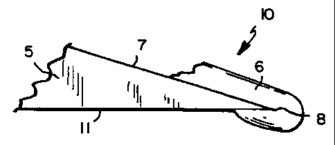
In a one embodiment of the present invention (FIG. 1), a metal cutting
edge blank 5 is formed by any method, e.g., powered cast metallurgy, forging,
coining, electric discharge machining, micro-machining, photo-etching, or the
li.ke. The blank 5, preferably, is formed with at least one tapered cutting
edge 7.
Thus, the cutting edge 7 is substantially less thick than the rest of the
blank 5.
The blank 5 is made of any thickness suitable for the cutting tool or surgical
instrument 10 that is desired.
The formed cutting edge blank 5 is cleaned and a coating 6 of a material
that is substantially harder than the material of the blank 5 is applied
thereto,
for example, by chemical vapor deposition, sputtering or ion-assisted
deposition. These processes, which are well known to those of ordinary skill
in
the art, typically utilize high vacuums in which the vacuum pressure is less
than 10-2 Torr, e.g., 10-3, 10-4, etc. The hard material coating 6 can be
formed
in the presence of suitable gaseous elements applied by the vacuum deposition
process. Indeed, it also is lmown to those skilled in the art that the
presence of
certain gasses assists in the adhesion of the coating 6 to the blank 5.
Suitable
hard materials for the deposited coating 6 are Si, A1203, ALTiN, TiN, SiC,
SiN,
MoS2, amorphous carbon, diamond-like carbon, zircon, and similar such
materials.
The coating 6 is applied so that a substantial layer of the harder material
continuously covers at least one side of the cutting edge 7 of the blank S.
Preferably, the coating 6 forms a continuous layer at the cutting edge 7.
Coatings 6 as thick as 30,000 A have been applied; but, usually, it is more
13
CA 02323259 2008-05-09
economical to apply a coating that is on the order of about 500 A or less.
Indeed, in the preferred embodiment, the thickness for the coating 6 after
focused ion milling is from about 100 A to about 500 A, more preferably at
least
about 200 A.
In an applicadon in which a coating 6 is desired on only one side, i.e.,
for the cutting edge 7 of a single-beveled cutting instrument 10, the coating
process typically deposits excess coating material 6 on the base surface 11,
which must be removed. Indeed, it is desirable to process the portion of the
blade that was not intended to be coated (i.e., the base surface 11), e.g., by
non-focused ion milling or ion etching, to remove the undesirable excess hard
material 6. Thereafter, the blank 5 is sharpened by focused ion beam (FIB)
milliag to create a new sharpened edge 9 having an atomically sharp edge. For
double-beveled cutting instruments, on which both sides of the blank are
tapered and coated with a harder material, each coated side of the blank is
milled by a focused ion beam to create a new sharpened end having an
atomically sharp double-beveled edge.
The focused ion beam removes portions of the coating 6 from the edge 7
and reestablishes a new, 'atoaeically sharp" cutting edge 9 (FIG. 2) that is
displaced by the remaining, i.e., non-milled, thickness of the coating 6 from
the
original cutting edge 7 of the blank S. U.S. Patent Number 5,945,677,
describes a process for providing a focussed
ion beam (FIB) that can be used for nanolithography. Such a FIB can be
14
CA 02323259 2000-10-12
focussed at an angle on the cutting edge of the coated blank 5 for removing
hard material 6 to form a new atomically sharp cutting edge 9.
Focused ion beam milling, as described above, is performed with
specialized equipment manufactured by Micrion Division of FEI or the like.
The focused ion beam 40, which forms the working energy source, preferably is
derived from an electrically excited liquid gallium source 45; however, other
ion sources 45 that are known to those slfllled in the art can be used without
deviating from the teachings of this invention. The source 45 emits a beam of
gallium ions 40 that are focused to a desired diameter. The focused beam 40 is
spatially limited, preferably, to about 5 nm in diameter. Larger focused beam
diameters, e.g., 10 nm, however, also can be used with satisfactory results.
The level of energy that is required to mill a sharp cutting edge 9 on a blade
blank 5 ranges from about 30 pA for a 5 nm diameter beam to about 100 pA for
a 10 nm diameter beam. As in any milling process, the object of this
- processing step is to remove (1) some or all specific areas of the harder
coating
6 along the desired cutting edge 9 and (2) in the plane of the base surface
11,
or, for double-beveled cutting edges, removing the hard coating along the
desired cutting edges.
The focused ion beam 40 cuts like an atomic milling machine, allowing
stress-free, in-situ sectioning to form an atomically-milled cutting edge 9.
The focused ion beam 40 is directed at the coating 6 on the blank 5 at
an angle within a few degrees of the desired final angle of the sharpened
CA 02323259 2000-10-12.
cutting edge 9. Typically, the beam 40 is directed toward the cutting edge 9
of
the blank 5 at an angle of about five (5) degrees greater than the reference
to a
plane parallel to the major surface of the blank cutting edge 9. The processes
of the present invention provide a cutting edge 9 having a high quality of the
surface finish and the repeatability of the dimensional tolerance of the
formed
product. It is preferred that the dimensional tolerance is accurate to at
least
0.3 microns, or less. Moreover, a radius of curvature of the cutting edge of
less
than about 300 A can be provided, preferably less than about 100 A, more
preferably less than about 10 A. Furthermore, by making the cutting edge in
accord with the present invention, microscopic debris is avoided at the
cutting
edge.
The cutting edge blank 5 having the new atomically sharpened edge is
finally joined to a support substrate (FIG. 7), which can be, e.g., metal or
plastic, which takes practically any shape or form and provides structural
support, strength, and shatter resistance to the resulting cutting edge 9. as
illustrated in FIG. 7, a double-beveled, atomically sharpened blank is mounted
to substrate 25 by means of adhesive (not shown). The substrate can be made
of any suitable material such as a metal or a plastic.
In a second embodiment, cutting edge blanks 60 are made from a wafer-
like sheet 65 of inetallic silicon, ceramic, glass, A1203, ALTiN, TiN, SiC,
SiN,
MoS2, amorphous carbon, diamond-like carbon, zircon, and similar such hard
material. cutting edge blanks having a variety of shapes can be fashioned from
a sheet 65, by micro-machining, non-focused ion beam milling, or etching
16
CA 02323259 2000-10-12
(FIGS. 5a and 5b), which processes ar.e well known to those of ordinary skill
in
the art. In this embodiment, a plurality of blanks 60 is first rough formed by
the said processes. The cutting edge blanks 60 are chemically etched to
provide a cutting edge 63 and are rough sawn to provide a back edge. Then,
the cutting edge 63 is sharpened by milling with a focused ion beam, as
described above, as necessary on one or two sides, to provide the desired
atomically sharp cutting edge. This embodiment can provide sharpened
cutting edges relatively quickly. The blanks with FIB milled sharpened edges
can be mounted on supports (e.g., see FIG 7) to provide cutting instruments.
Rectangular blanks 61, which are made by micro-machining, etching or
non-focused beam milling, are the preferred shape; however, e.g., circular,
elliptical, triangular, and polygonal shapes are within the teaching of this
invention. To form the rectangular blanks 61, micro-machining, etching or
non-focused beam milling is performed in such a manner as to define the
perimeter of the rectangular blank 61. The taper angle 62 of the cutting edge
63 of the rough blank 61 typically is between about 30 and about 60 degrees,
preferably about 36.8 degrees as shown in FIG. 5b. The rectangular blank 61
is then milled with a focused ion beam to create an atomically sharp cutting
edge at 63. The individual cutting edge blanks 60 can be, e.g., halved 69 from
the rectangular blanks 61. As an example, in Figure 5a, a rectangular blank
61 is halved 69 to produce a pair of cutting edged blanks 60 with three
atomically sharp cutting edges 63. The cutting edge can be provided in any
shape. A support substrate, e.g., of metal plastic, glass, etc., is then
laminated
17
CA 02323259 2000-10-12
to the cutting edged blank 60 to provide structural support, strength, and
shatter resistance.
In another embodiment (FIG. 3a), a plurality of blade cutting edge blanks
30 are fabricated from wafers 35 of, e.g., silicon, ceramic, glass, A1z03,
ALTiN,
TiN, SiC, SiN, MoS2, amorphous carbon, diamond-like carbon, zircon, and
similar such hard material, preferably materials that are readily available in
the
form of wafers from the semiconductor industry. Preferably, the wafer 35
thickness is between about 100 m and about 1000 um. More preferably, at
least one side 38 of the wafer 35 is polished to an atomic finish, which
feature
is also common in the semiconductor industry.
Initially, a wafer-dicing saw 32 is used on the wafer 35 to provide a
rough geometry for the cutting edge blank 30. Indeed, the object of the dicing
operation is to form, or create, a series of elongated cutting edge blanks 30,
e.g., triangular prism shaped components, across the surface of the wafer 35.
Before dicing, the wafer 35 is mounted securely in a fixture and, then, a
cutting
saw 32 systematically produces a plurality of blanks 30. The cutting saw 32 is
equipped with a specially prepared blade 39 (e.g., diamond, silicon carbide,
or
the like) with a cutting face of about 100 m. The specially prepared blade 39
of the cutting saw 32 is capable of forming precision cut bevels in the wafer
35
wherein the peaks being formed have an included angle ranging preferably
from about 10 to about 90 degrees; however, the cutting media of the saw 32
is selected so that it does not produce chips greater than 0.3 m in
dimension.
18
CA 02323259 2000-10-12
After the sawed wafer 35 is cut into cutting edge blanks 30, it is cleaned,
e.g. by ultrasonic cleaning, plasma, high-pressure de-ionized water, and the
like, to remove all debris and cutting solvent that may have contaminated the
surface. The cutting edge blanks 30, then are loaded into a vacuum chamber
of a focused ion beam mill. The chamber is exhausted to a vacuum pressure of
about 10-7 Torr. Then a focused ion beam 40 is directed along at least one
side
31, 33 toward the apex 34 of the blade blank 30 (FIG. 3B).
Cutting edge blanks can also be made by chemical etching techniques,
which are well known to those slfl.lled in the art. For example, a silicon
wafer is
provided with a photoresist mask, which is resistant to the etching solution
being used. The mask consists of longitudinal strips of resist located at the
position of top blade edge of the cutting edge blank, i.e., the apex of the
cutting
edge blank having a height perpendicular to the plane of the wafer. For an
etching depth in the wafer of 150 microns, it is necessary to provide at least
a
one micron wide strip of resist along the top blade edge to prevent under
etching and damage to the edge structure. The final edge is shaped by the FIB.
Depending on the desired final use and/or the ultimate radius of
curvature, i.e., edge sharpness, the focus ion beam 40 can be directed at the
blade blank 30 from in front of the leading edge 50 or from behind the leading
edge 50 (FIG. 3B). Ultimate sharpness is created when the focused ion beam
source 45 preferably is applied to the cutting edge 50 from behind the leading
edge of the cutting edge blank 30. Sharpened edges having included angles of
19
CA 02323259 2000-10-12
from about 10 to about 70 are preferred. Thus, FIB angles of from about 5 to
about 70 typically are used.
Preferably, an edge having polished side 38 adjacent thereto is used and
the FIB is directed from an opposite side 31 to provide the atomically
sharpened single bevel edge.
Once the desired atomically sharp edge 50 has been produced on the
cutting edge blank 30, the base of the cutting edge blank 30 (opposite the
sharpened edge, e.g., side 33) is fixedly attached to a support substrate
(e.g.,
see FIG. 7), that is made, e.g., of metal, plastic, glass, ceramic or the like
by
means of, e.g., solder, epoxy, brazing, staking, crimping, adhesives, friction
fitting or eutectic bonding. The support substrate facilitates ultimately
attaching the mounted, atomically sharp cutting edge blank 30 to any desired
cutting instrument or tool body. It also is possible to practice this
invention by
attaching the sharpened blade blank 30 directly to the cutting instrument or
tool body.
For a double beveled cutting edge, the FIB is directed from both sides of
the cutting edge.
Using the focused ion beam mechanism in the transverse, high current
mode, it is possible to sculpt various edge geometries by a process referred
to
as "beam shaping". The focused ion beam for "beam shaping" has a preferred
beam diameter of at least about 10 nm.
CA 02323259 2000-10-12
FIGs. 4A-4E illustrate the edges of prior art blades mechanically
sharpened and honed to provide extreme sharpness for microsurgical
instruments. FIG. 4A shows a typical defect in the sharpened edge. FIGs. 4B-
4E show typical rollover of metal at the sharpened edge and microscopic debris
left by the mechanical sharpening and honing processes.
FIG. 6 graphically demonstrates the dramatic improvement in sharpness
resulting from focused ion beam milling. FIG. 6 depicts two areas on a blade
edge. The first area 52 has been sharpened with conventional abraded
grinding and honing of the edge. It has microscopic debris around the
sharpened edge and the edge, itself, shows rollovers. The second area 54 has
been milled with a focused ion beam 40 in accord with the present invention.
Note the surprisingly clean surfaces around the sharpened edge and the clean
atomically sharp edge.
The invention has been described in detail including preferred
embodiments. However, it is appreciated that, upon consideration of this
disclosure of the specification and the drawings, those slfllled in the art
may
make changes, additions and/or i.mprovements within the spirit and scope of
the invention.
21