Note : Les descriptions sont présentées dans la langue officielle dans laquelle elles ont été soumises.
CA 02325250 2000-11-08
Aksyuk 24-49-58 1
OPTICAL CROSSCONNECT USING TILTING MIRROR MEMS ARRAY
BACKGROUND OF THE INVENTION
1. Field of the Invention
The present invention pertains to fiber optic communications systems and,
more particularly, to optical crossconnect configurations utilizing micro
electromechanical systems (MEMS) tilting mirror arrays.
2. Description of the Related Art
In fiber optic communication systems, signal routing is essential for
directing an optical signal carrying data to an intended location. Existing
routing
techniques typically experience optical power loss due to inefficient coupling
of optic
signals between input and output fibers. This increases the dependence on
optical power
sources (e.g., pump lasers) which are used to compensate for power losses by
injecting
optical power back into the optical system. The need for optical power sources
increases
the overall cost of the optical system.
Another criteria for signal routing is the ability to direct a signal received
from one of a plurality of input fibers or ports to any of a plurality of
output fibers or
ports without regard to the frequency of the optical signal. Known optical
signal routers
are frequency dependent so that frequency dictates the routing of multiple
signals, each
signal having a discrete wavelength, to output ports based on the signal
frequency. For
example, and as disclosed in commonly-owned U.S. Patent Application Serial No.
09/414,622, filed October 8, 1999, multiple adjacent-in-frequency wavelengths
will be
routed to adjacent-in-space output fibers, as opposed to randomly selected
output fibers.
Accordingly, an optical crossconnect system is desired having flexible
frequency routing
capability with reduced power loss.
CA 02325250 2000-11-08
Aksyuk 24-49-58 2
SUMMARY OF THE INVENTION
Improvements over known optical crossconnects are realized by
providing an optical crosssconnect utilizing an array of tilting micro-
electromechanical
systems (MEMS) mirrors for directing optical signals from input optic fibers
to output
optic fibers. The optical crossconnect includes a lens array for receiving
optical signals
from a plurality of input fibers. The lens array is made of up a plurality of
lens
elements, with each lens element directing or focussing an optical signal to a
MEMS
mirror array. The MEMS mirror array includes a plurality of mirror elements,
each
being tiltable about one or more rotational aces upon the application of
control signals to
the desired mirror elements. In this manner, optical signals can be directed
along
various paths and to various output fibers.
In a preferred embodiment, input and output lens arrays are used in
conjunction with input and output MEMS mirror arrays. The input lenses direct
input
optical signals to the input MEMS array which, in turn, reflects each signal
in a direction
relative to each mirror's tilt orientation. The reflected signals are received
and further
reflected by the output MEMS mirror array to the output lens array for
coupling to
output fibers.
In another preferred embodiment, input and output lens arrays are formed
on a common substrate, with a reflective surface disposed therebetween, and
input and
output MEMS mirror arrays are formed on a second common substrate disposed in
opposing relation to the first substrate. The reflective surface receives
reflected optical
signals from the input MEMS array and directs them to the output MEMS array.
In yet another embodiment, an optical element having transmissive
properties is disposed in optical communication with a first MEMS mirror array
and a
second MEMS mirror array. The optical element directs optical signals, either
by
transmission or reflection, between the first and second mirror arrays to
selectively
forward optical signals between a first fiber array and a second fiber array.
CA 02325250 2000-11-08
Aksyuk 24-49-58 3
Other objects and features of the present invention will become
apparent from the following detailed description considered in conjunction
with the
accompanying drawings. It is to be understood, however, that the drawings are
designed solely for purposes of illustration and not as a definition of the
limits of the
S invention, for which reference should be made to the appended claims. It
should be
further understood that the drawings are not necessarily drawn to scale and
that,
unless otherwise indicated, they are merely intended to conceptually
illustrate the
structures and procedures described herein.
BRIEF DESCRIPTION OF THE DRAWINGS
In the drawings, wherein like reference numerals denote similar elements
throughout the several views.
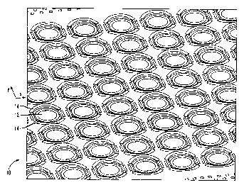
FIG. 1 is a planar view of an example of a MEMS mirror array used in
connection with the present invention;
FIG. 2 is a schematic representation of an optical crossconnect in
1 S accordance with one embodiment of the present invention;
FIG. 3 is a schematic representation of an alternative embodiment of the
optical crossconnect of FIG. 2;
FIG. 4 is a schematic representation of yet another embodiment of the
optical crossconnect of FIG. 2; and
FIG. 5 is a schematic representation of a "folded" optical crossconnect in
accordance with still another embodiment of the present invention.
DETAILED DESCRIPTION OF THE PRESENTLY PREFERRED
EMBODIMENTS
Arrays of two-axis tilt mirrors implemented using micro-
electromechanical systems (MEMS) technology allow for the construction of
large scale
optical crossconnects for use in optical systems. Optical crossconnects are
employed to
connect a number of input optical paths to a number of output optical paths.
Typical
requirements of optical crossconnects are that any input be capable of being
connected to
' CA 02325250 2000-11-08
Aksyuk 24-49-58 4
any output. One example of a MEMS mirror array 10 is depicted in FIG. /. The
mirror array 10 includes a plurality of tilt mirrors 12 mounted to actuation
members or
springs 14 and controlled by electrodes (not shown). Each mirror 12 is
approximately
100-500 Microns across, may be shaped as square, circular or elliptical, and
is capable
of rotating or tilting about X-Y axes, with the tilt angle being determined by
the amount
of voltage applied to the electrodes. Further details of the operation of the
MEMS
mirror array 10 is found in U.S. patent application Serial No. 091415,178,
filed October
8, 1999, the entire contents of which are incorporated herein by reference.
The general
concept of utilizing two or more such tilt mirror arrays 10 to form an optical
crossconnect is disclosed in U.S. patent application Serial No. 09/410,586,
filed October
1, 1999, the entire contents of which are also incorporated herein by
reference.
Applicants have discovered that by utilizing one or more MEMS tilt
mirror arrays in conjunction with a lens array, various optical crossconnect
configurations can be realized of compact size (i.e. minimal spacing between
crossconnect components) and exhibiting minimal optical power loss. One such
optical
crossconnect 100 in accordance with a currently preferred embodiment of the
invention
is depicted in FIG. 2. Crossconnect 100 receives input optic signals 108
through a
plurality of optic fibers 112, preferably formed in an array as is well known
in the art.
For ease of illustration fiber array 112 is shown as a one-dimensional array
having four
fibers 112a, 112b, 112c, 112d. It is in any event to be understood that fiber
array 112 as
well as other fiber arrays discussed herein are preferably two-dimensional N x
N arrays.
Fiber array 112 transmits the optical signals 108 to an array of lenses 114
preferably functioning as collimating lenses. The lens array 114 is positioned
relative to
the fiber array 112 so that each lens communicates with a corresponding fiber
for
producing pencil beams 116 from the optic signals 108. Thus, beam 116a is
produced
from a signal carried by fiber 112a, beam 116d is produced from a signal
carried by
fiber 112d, etc.
CA 02325250 2000-11-08
Aksyuk 24-49-58 5
A first MEMS tilt mirror array 118, also referred to as an input array, is
positioned in alignment with the lens array 114 so that each mirror element 12
(FIG. 1)
will receive a beam 116. The mirror elements are tilted, in a manner discussed
in
application Serial No. 09/415,178, to reflect the beams 116 to a second or
output MEMS
mirror array 122 positioned in optical communication with MEMS array 118.
Depending on the tilt angle for each mirror element in the input MEMS array
118, the
reflected signals can be selectively directed to specific mirror elements in
the output
MEMS array 122. To illustrate this principle, beam 116a is shown generating
reflection
beams 120a and 120a' and beam 116d is shown generating reflection beams 120d
and
120d'. These beams are received by mirror elements in the output MEMS array
122 and
are directed as beams 124 to an output lens array 126. An output fiber array
128 is
aligned with the lens array 126 to receive and output optical signals 129.
Thus, lens
array 126 couples beams 124 into the output fiber array 128.
The crossconnect device 100 contains a 1-to-1 mapping of each output
fiber to a mirror in the output mirror array. This is required with single
mode fibers
because of the small numerical aperture which necessitates coaxial alignment
of the input
and output beams with the fiber axes to achieve low power loss. The
crossconnect of
FIG. 2 allows for adequate spacing of the fiber and mirror arrays to limit the
required
mirror angle excursions.
A typical spacing dimension which will result in reduced diffraction
losses is between 50-100 mm. If the mirror, lens and fiber arrays are
coplanar, i.e.
input fiber array 112, input lens 114 and output mirror array 122 are coplanar
with each
other, and output fiber array 128, output lens array 126 and input mirror
array 118 are
coplanar with each other, thus two similar monolithic blocks may be formed.
Assembly
of the crossconnect will then only require one six-axis alignment.
Another crossconnect configuration 200 in accordance with the invention
is illustrated in FIG. 3. Like the crossconnect 100 of FIG. 2, crossconnect
200 contains
an array of input lenses 214, and an array of output lenses 226 which
communicate
CA 02325250 2000-11-08
Aksyuk 24-49-58 6
optical signals through an input fiber array 212 and an output fiber array
228,
respectively. Input and output MEMS mirror arrays 218 and 222 are spaced apart
from
lens arrays 214, 226 for directing optical signals between the input fiber
array and output
fiber array. Unlike crossconnect 100, the device in FIG. 3 has the MEMS mirror
arrays
S and lens arrays positioned on opposite sides of the crossconnect fabric,
which allows for
ease in construction. In particular, the mirror arrays can be monolithically
integrated on
a first common substrate and the lens arrays and fiber arrays monolithically
integrated on
a second common substrate. To provide for signal routing between the MEMS
mirror
arrays, the lens arrays 214, 226 are formed on a common substrate and spaced
apart
from each other so that a reflective element 230 can be disposed therebetween.
Reflective element 230 may be a separate plane mirror or, preferably, a
reflective
coating material (e.g. gold) deposited on the lens substrate and positioned
for
communicating optical signals between mirror array 218 and mirror array 222.
Once the
lens arrays are in place, crossconnect 200 requires a single six-axis
adjustment of the
coplanar mirror arrays.
Turning now to FIG. 4, a variation of the crossconnect of FIG. 3 is
shown as crossconnect 300. A primary difference from the embodiment of FIG. 3
is the
removal of reflective element 230. As shown, mirror arrays 318 and 322 are
angled
relative to the substrate planes containing lens arrays 314 and 326 so that
the optical
signals can be communicated directly between the mirror arrays. In this
embodiment,
the maximum distance between each fiber array (e.g., array 312) and its
opposing mirror
array (e.g., array 318) can be small. This is an important design
consideration,
especially if the pointing accuracy of the fiber array is poor. The mirror
elements in the
mirror arrays can be used not only to adjust the switch connects (e.g., a
routing function)
but also to compensate for imperfections in the fiber array.
FIG. 5 depicts another crossconnect 400 which employs a plane mirror
430 in an offset configuration relative to a single MEMS mirror array 420. In
this
further embodiment, a single fiber array 410, single lens array 416 and single
MEMS
CA 02325250 2000-11-08
Aksyuk 24-49-58 7
mirror array 420 are used in a "folded" crossconnect arrangement. The single
fiber
array functions as a combined inputJoutput array. An input signal 412 is
provided to
lens array 416 by fiber 414 for imaging on a mirror element 420a. The beam is
then
reflected to plane mirror 430 and reflected back to mirror element 420b for
output
through lens array 416 to output fiber 422. It should be noted that in this
configuration,
there is no distinction between input and output ports. Thus, with a 32 x 32
mirror array
with one port unused, the crossconnect can be used as a 1 x 10²³ switch, an
array of 341
1 x 2 switches, or a 512 x 512 optical crossconnect. Other variations of
course exist, as
do other mixtures of crossconnect components (e.g. two 1 x 128 switches, sixty-
four 2 x
2 switches and one 256 x 256 switches may be used with a 32 x 32 mirror
array).
Thus, while there have shown and described and pointed out
fundamental novel features of the invention as applied to preferred
embodiments
thereof, it will be understood that various omissions and substitutions and
changes in
the form and details of the devices illustrated, and in their operation, may
be made by
those skilled in the art without departing from the spirit of the invention.
For
example, it is expressly intended that all combinations of those elements
which
perform substantially the same function in substantially the same way to
achieve the
same results are within the scope of the invention. Moreover, it should be
recognized
that structures and/or elements shown and/or described in connection with any
disclosed form or embodiment of the invention may be incorporated in any other
disclosed or described or suggested form or embodiment as a general matter of
design
choice. It is the intention, therefore, to be limited only as indicated by the
scope of
the claims appended hereto.