Note : Les descriptions sont présentées dans la langue officielle dans laquelle elles ont été soumises.
CA 02327031 2006-05-30
Title: COMPOSITE VAPOUR DEPOSITED COATINGS AND PROCESS
THEREFOR
FIELD OF INVENTION
This invention is related to hard, wear resistant coatings vapour deposited
over a
metallic or non-metallic surface, in particular to tools utilized in
industrial, medical and dental
cutting, and form scraping.
BACKGROUND OF THE INVENTION
Hard wearing surfaces are in common use in various industries, and such hard
wearing surfaces are frequently obtained by coating the surface of a tool made
of steel or
similar metal, or other hard, enduring material, with a layer of hard wearing
ceramic
substance, such as carbides, nitrides and carbonitrides, or providing a hard
microcrystalline
diamond coating. There are known methods for obtaining hard wearing coatings,
such as for
example, having a coating of diamond particles in combination with a carbide
or nitride layer
and then filling the gaps between the abrasive particles with a softer
intermetallic compound.
Another known method is vapour deposition of hard-wearing ceramic materials
from plasma
or by utilising molten ceramic substances. Hard wearing surfaces for use on
medical, surgical
and dental tools have additional requirements, as such surgical and dental
tools need to be
frequently sterilised, hence medical tools have to be corrosion resistant. A
device for yielding
hard ceramic surfaces by cathodic arc plasma deposition is described in U.S.
4,851,095,
issued to M.A. Scobey et al. on July 25, 1989. The apparatus of Scobey et al.
utilises a high
intensity ion flux. Vapour deposition of a hard ceramic material, such as
titanium or
zirconium nitride on a stainless steel or titanium surface by utilizing a
molten evaporant and a
hollow cathode, is described in U.S. patent 5,152,774, issued to W.A.
Schroeder on October
6, 1992. The vapour deposition of Schroeder is conducted at relatively low
temperature, thus
the substrate will have lost little of its initial high strength properties,
however, the
requirement of low surface roughness of the deposited layer is not addressed
by U.S.
5,152,774. In U.S. 4,981,756, issued to H.S. Rhandhawa on January 1, 1991, a
method is
taught to coat surgical tools and instruments by cathodic arc plasma
deposition. The ceramic
coating obtained by this technology is a nitride, carbide or carbonitride of
zirconium or
hafnium, in a single layer of 3-10 m thickness. U.S. 4,981,756 also refers to
various
publications describing knovai equipment for obtaining hard-wearing surfaces
by cathodic arc
plasma deposition. U.S. patents 5,940,975 and 5,992,268 issued to T.G. Decker
et al. on
August 24, 1999 and November 30, 1999, respectively, teach hard, amorphous
diamond
coatings obtained in a single layer on thin metallic blades or similar
metallic strips utilizing
filtered cathodic arc plasma generated by vaporizing graphite. It is noted
that no interlayer is
formed between the blade surface and the deposited amorphous diamond coating.
CA 02327031 2000-11-28
It is known to have titanium and titanium nitride coated dental tools and
surgical
instruments wherein the coating is obtained by conventional cathodic arc
deposition applied
to corrosion resistant stainless steel substrates. The cutting surfaces of
such medical tools
need to be smooth, as well as hard-wearing to prevent trapping and retaining
materials which
can be harmful to the patient. Hence, another requirement is that the cutting
edges be very
straight, sharp and nick-free to avoid damage to the surrounding flesh and
skin during dental
treatment. There are known methods described, wherein the cutting tips of
surgical
instruments made of steel have been sand-blasted and then coated with a hard-
wearing
cerainic composition, however this method may, or is likely to increase
surface roughness
and unevenness, rather than eliminate it. The grain size of deposits obtained
in conventional
cathodic plasma arc methods may range between 0.5 to 10 m. Any post-deposition
heat
treatment which may be required to maintain corrosion resistance of the
substrate, may lead
to internal stresses in the coating due to differences in the grain size, and
can eventually lead
to abrasion, spalling, crack formation, grain separation, surface fractures,
uneven edges and
rough surfaces, and such like, which can drastically reduce the wear
resistance and durability
of surgical instruments and dental tools. None of the above discussed methods
are concerned
with even grain size and surface structure, and low micro-roughness of the
vapour deposited
hard, ceramic coatings, which have particular importance for dental and
surgical tools, and in
other applications where straight, sharp, even and nick-free edges are
essential requirements.
There is a need for a method to obtain fine grained, hard wearing ceramic
surfaces
having low micro-roughness, sharp even edges, which can also withstand post-
deposition
heat treatment without detriment and degradation of the coating.
SUMMARY OF THE INVENTION
An object of the invention is to obtain a coating made of alternating metal
and metal
ceramic layers of relatively even surface structure and grain size over a
requisite surface area
of a hard substrate. The coating is obtained by first cleaning, then
optionally ion nitriding the
surface of a steel, titanium, carbide or similar hard substrate, and
subsequently vapour
depositing in a cathodic arc plasma deposition device alternating metal and
ceramic layers
utilizing a magnetically filtered cathodic arc plasma. The magnetic filtration
regulates the
evenness of the grain size of the deposited layer, and thus a hard-wearing
surface having low
micro-roughness can be obtained.
According to one embodiment of the present invention a wear resistant,
composite
vapour deposited metal ceramic coating is provided on a substrate capable of
electrical
conduction. The coating includes at least one metallic layer selected from the
group
consisting of titanium, chromium, vanadium, aluminum, molybdenum, niobium,
tungsten,
2
CA 02327031 2000-11-28
hafnium, zirconium and alloys thereof and having a metallic layer thickness.
The coating
further includes at least one ceramic layer selected from the group consisting
of nitrides,
carbides, carbohydrides, oxycarbides and oxynitrides. The composite, vapour
deposited
metal-ceramic coating has a thickness greater than not .25 m, a micro-
roughness less tha:n the
total thickness of the uppermost ceramic layer, and a micro-hardness in excess
of 20GPa.
The substrate may be of steel. The steel may have an ion nitrided surface
layer
between it and the composite vapour deposited metal-ceramic coating.
The composite vapour deposited coating may have at least one pair of a metal
layer
and a ceramic layer having a common metal ion component.
The vapour deposited coating may comprise a multiplicity of pairs of metal and
ceramic layers having a common metal ion component.
The composite vapour deposited metal-ceramic coating may be heat treated
subsequent to deposition.
The coating thickness may range between 0.25 m and 204m.
The thickness of the metal layer may range between 0.05 m and 0.5 m.
The vapour deposited metal-ceramic coating may comprise a portion of a surface
of a
dental tool, a surgical tool or a cutting tool.
A process is provided for producing a wear resistant, composite vapour
deposited
metal-ceramic coating on the surface of the substrate capable of electrical
conduction, the
process comprise of the steps of:
i) providing a substrate capable of electrical conduction, having a surface
and cleaning
said surface by applying at least one cleaning method selected from the group
consisting of
chemical cleaning, electrolytic cleaning, grinding, polishing, and ion
bombardment to
produce a cleaned substrate;
ii) placing said cleaned substrate in the vacuum chamber of a vapour
depositing
device capable of providing controlled electric and magnetic fields and having
a substrate
holder capable of holding at least one substrate, a target electrode holder
and an inlet for a
vapour depositing atmosphere of controlled composition and pressure;
iii) providing a target electrode within said vacuum chamber, of one of the
metals
selected from the group consisting of titanium, chromium, vanadium, aluminuin,
molybdenum, niobium, tungsten, hafnium, zirconium, and alloys thereof;
iv) providing a vapour depositing atmosphere within said vacuum chamber,
comprising at least one of the gases selected from the group consisting of
argon, nitrogen,
methane or other hydro-carbon gas and oxygen.
v) optionally treating said surface of said substrate in an ion nitriding
process step;
3
CA 02327031 2000-11-28
vi) applying electric potential and a filtering magnetic field in an argon
atmosphere
within said vacuum chamber, to obtain a first, vapour deposited metal layer
selected from the
group consisting of titanium, chromium, vanadium, aluminum, molybdenuin,
niobium,
tungsten, hafnium, zirconium, and alloys thereof, on said surface of said
substrate;
vii) applying electric potential and a filtering magnetic field in an
atmosphere within
said vacuum chamber, containing at least one of the gases selected from the
group consisting
of nitrogen, methane, oxygen and water vapour, to obtain a second, vapour
deposited layer of
a ceramic compound of a metal selected from the group consisting of titanium,
chromium,
vanadium, aluminum, molybdenum, niobium, tungsten, hafnium, zirconium, and
alloys
thereof, on said first layer deposited on said surface of said substrate;
viii) repeating steps vi) and vii), thereby obtaining a third, vapour
deposited metal
layer and a fourth, vapour deposited ceramic compound layer on said surface of
said
substrate;
ix) removing said substrate having at least four vapour deposited layers on
said
substrate surface, from said vapour depositing device; and
x) heat treating the obtained vapour deposited coating comprising at least
four vapour
deposited layers on said substrate surface.
Steps vi) and vii) may be repeated to provide a fifth, vapour deposited metal
layer and
a sixth vapour deposited ceramic compound layer on the surface of the
substrate prior to the
heat treatment.
Steps vi) and vii) may be repeated to provide a first multiplicity of vapour
deposited
metal layers and a second multiplicity of vapour deposited ceramic compound
layers on the
surface of the substrate prior to the heat treatment.
The substrate may be of steal.
BRIEF DESCRIPTION OF THE DRAWINGS
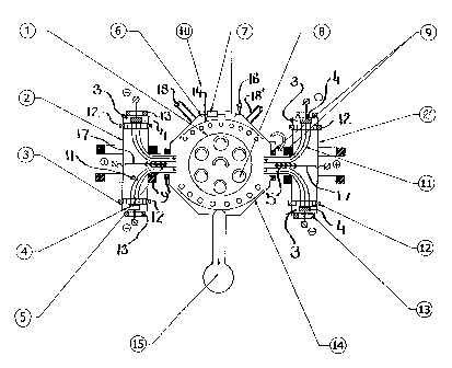
Fig. 1 is a schematic drawing of the cathodic arc plasma depositing device
utilized in
this invention.
Fig.2 is a schematic drawing of the cross-section of a multi-layered vapour
deposit
obtained in accordance with the present invention.
Fig.3a and 3b show the surface roughness of a vapour deposit obtained by
conventional methods and by the present method, respectively.
A detailed description of the preferred embodiments of the invention will
follow,
illustrated by working examples.
DETAILED DESCRIPTION OF THE PREFERRED EMBODIMENTS
4
CA 02327031 2000-11-28
As discussed above, providing a vapour deposited coating of hard-wearing
particles
on a metal or similar hard surface such as, for example, a carbide, nitride or
boride surface, is
known. One difficulty frequeintly encountered is that the deposited hard-
wearing particles,
especially when such have a wide variation in size, may become loose and
detached from the
surface. To eliminate such problems the hard-wearing particles can be coated
with a another
hard-wearing material or/and the composite layer can be coated with a softer
material to
increase adhesion of the different particles to one another and to the
substrate surface.
For the sake of clarity, definition of what is understood by some of the
terminology
used in the discussion of the preferred embodiments of the present invention
is provided
below.
"Substrate" is understood to mean a three dimensional body providing the
surface on
which the vapour species is deposited. Only a portion of the surface, usually
the surface in
the proximity of one end of the substrate body, is utilized as the depositing
surface, and the
other end of the body of the substrate is attached to or is supported by, a
substrate mount or
holder. It is preferred that the portion of the surface on which the deposit
is to be obtained,
has close to uniform temperature, while the rest of the substrate may be in a
temperature
gradient.
"Plasma" is considered to mean an atmosphere of low pressure and high
temperature,
containing ionised gaseous species. Not all the gases in the plasma are
ionised, but it is usual
that the species to be deposited is ionised. The components of a plasma often
include argon
or similar inert gases, both in the atomic state and in an ionised state.
"Even surface" in the context of a deposited layer surface is understood to
mean that the
average distance between the peaks of the deposited surface and the valleys of
the deposited
surface, is small. In other words, the micro-roughness of an evenly deposited
surface is
considered to be low.
In one embodiment of the present invention multiple layers of a controlled
thickness of
a metal and of a hard-wearing ceramic compound of the same metal, are
deposited in
successive steps on a conductive substrate surface, usually a stainless steel
surface. It is
preferred that at least two pairs of the metal layer and the hard-wearing
ceramic layer are
deposited on the steel substrate. The number of layer pairs constituting the
coating may range
from 2 to as high as 6 or even 7, depending on the desired coating thickness,
and on economic
considerations.
The vapour deposition process of the present invention utilizes plasma
technology in
conjunction with a cathodic arc source. In the following a brief and
simplified description of
this technology will be provided, however, it should be understood that this
is given rnerely to
allow clarification of the process parameters and is not intended as an
accurate scientific
description of the mechanisms involved in cathode arc technology. In cathodic
arc technology
5
CA 02327031 2006-05-30
metal droplets and metal vapour are generated by applying an arc of high
current to a
negatively charged target metal in a vacuum chamber. At the same time, high
concentrations
of electrons are also released from the target metal cathode at high speed.
The vacuum
chamber, by definition, contains a gas at a low pressure, and it is usual that
the gas is fed to the
chamber as a plasma containing a gas or a gas mixture at high temperature in a
partially ionised
state. The high speed electrons collide with the gas molecules, thereby
further ionising the gas
molecules, which in turn collide with and ionise the metal droplets and metal
vapour. The
ionised gas and the ionised metal vapour and metal droplets proceed towards
the negatively
charged substrate also located in the vacuum chamber. The metal deposits in a
layer over the
surface of the substrate. When the gas is an inert gas no reaction takes place
between the
ionised gas and metal vapour. On the other hand, in the instance of the plasma
also containing
reactive gases, the ionised gases will react with the metal vapour, forming a
deposited ceramic
compound layer. In conventional cathodic arc plasma deposition the vaporised
metal droplets
in the plasma can vary in size, thus the metal or the ceramic compound
deposited on the
substrate is likely to exhibit widely varying grain sizes and surface
unevenness.
In a recent modification of plasma technology deposits are obtained by
filtering a
cathodic arc source by means of appropriately adjusted magnetic fields. An
example of such a
cathodic arc plasma coating apparatus is described in U.S. patent 5,435,900
issued to V.I.
Gorokhovsky . The large area dual filtered arc
depositing apparatus which can be used in practising the present invention is
shown
schematically in Fig.l. The arc depositing apparatus 10, contains a main
vacuum chamber 6,
housing a substrate platform 1, bearing double or triple rotating satellites
8, which are utilized
in supporting substrates providing appropriate depositing surfaces. Substrate
platform 1 is
connected to a negative bias voltage power supply for rendering the substrate
surfaces receptive
of ions during the deposition process. Two plasma guide chambers 2 and 2' are
located on
opposing sides of vacuum chamber 6, each enclosing two large area dual
filtered cathodic arc
sources 3, appended to flanges within the plasma guide chamber. Thus the
vacuum chamber 6
contains altogether four cathodic arc sources 3, but only one of those is
described in detail. In
the preferred arrangement two cathodic are sources 3 are utilized, located at
opposing flanged
ends of the plasma guide chamber 2, each having a metal target electrode 4.
The metal target 4,
is connected to the negative pole of a low voltage high current power supply,
thus being
capable of generating separate metal vapour jets which converge into metal
plasma stream 11.
The metal vapourjets are focussed and steered by magnetic coils 12 and 13.
Deflecting coils 9
bend and collimate plasma streams 11 to direct the flow towards the substrate
depositing
surfaces. Metal droplets of larger size, and most of the non-ionised neutral
species are trapped
on baffles 5, of anode-separators 17. Anode-separators 17, bear a positive
potential relative to
the plasma streain and thus repel the positively charged ions, urging such
ions towards the
substrates. Vacuum chamber 6, is equipped with a front door 16, for loading
the substrates to
be coated. Front door 16, also has view ports and flanges 7, for diagnostic
assessment and
6
CA 02327031 2000-11-28
control of the deposition process. On the perimeter of the vacuum chamber,
preferably
opposite front door 16, is located vacuum pumping system 15, which is not
shown in detail.
The vacuum chamber 6, also has gas entry ports 18 and 18'. When the deflecting
coils are not
activated, the cathodic targets 4, serve as powerful electron emitters,
thereby providing high
electron currents between the cathodic targets and auxiliary anodes 14. This
arrangement
creates a highly ionised gaseous environment during all stages of the process:
ion cleaning, ion
nitriding and deposition of coating layers. In addition, some form of heaters
can be connected
to the auxiliary anodes 14, to allow the temperature of the depositing surface
of the substrate to
be controlled independently. It is noted, however, that the apparatus of Fig.l
is merely an
example of a device utilizing magnetic plasma arc filtering. Any other high
temperature
vapour depositing apparatus which is fitted with magnetic plasma arc filtering
means may be
employed in practising the present invention. It is also noted, that the
preferred vapour
depositing device contains an arrangement with four cathodic targets, however,
it is possible to
operate the device with only two cathodic targets.
The application of magnetic filtering of the cathodic are stream eliminates
droplets of
larger sizes, as well as neutral non-ionised species, and thereby
substantially only ionised metal
vapour and nano-sized metal droplets carrying a charge, will reach the
substrate. This results in
deposit layers of even grain size, and surfaces having very low micro-
roughness. Such surfaces
may be referred to as evenly deposited surfaces.
The substrate selected for deposition in the present process is a conductive
material,
such as a metal or a hard-wearing substance having relatively high electrical
conductivity. In
one of the preferred embodiments the substrate is stainless steel of the ASA
400 series.
The substrate surface to be coated is first cleaned, by usual cleaning
processes
which can include grinding, polishing, chemical cleaning, degreasing,
electrolytic cleaning, ion
bombardment or similar conventional cleaning steps which can render the
surface receptive of
the deposited substance.
The cleaned substrate can optionally be ion nitride to increase the hardness
and
corrosion resistance of the substrate surface and possibly further improve
adherence of the
deposited coating. The ion nitriding may be conducted in a separate apparatus,
or the plasma
arc depositing device shown on Fig.1 can be adapted to the ion nitriding
process step.
The substrate having a cleaned, and optionally nitride depositing surface, is
then
placed in the vacuum chamber of a suitable cathode arc plasma depositing
device having
magnetic filtering means, such as described above. The target cathode selected
for the cathodic
arc generation, is a metal which is capable of forming hard, wear resistant
compounds by
vapour deposition. The metals which are preferred in such compound formation
are titanium,
chromium, vanadium, molybdenum, aluminum, hafnium, zirconium, niobium,
tungsten, their
ailoys, and metals of similar nature.
The gas atmosphere in the cathodic arc depositing device is controlled such
that
it can yield either a vapour deposited metal layer or a vapour deposited
ceramic compound
7
CA 02327031 2000-11-28
layer. The ceramic compounds that have desired wear resistance and hardness
are the carbides,
nitrides, carbonitrides, oxycarbides and oxynitrides of the above listed
metals. The plasma for
depositing the desired ceramic layers contains one or more of the following
gases: nitrogen,
methane or other hydro-carbon gas and oxygen. In the vapour deposition of
layers of the above
listed metals only argon, or similar inert gas containing plasma is used.
Argon may also be
utilized to dilute or carry the gases reacting with the metal vapour or metal
deposit, to form the
desired ceramic compounds. The metal and ceramic compound combinations
suitable for
forming hard, wear resistant coatings by vapour deposition in the present
invention, are listed
in Table 1 below.
The first metal layer to form a metal-ceramic compound layer pair, is obtained
by having one of the metals listed above as cathodic target metal. The metal
layer is deposited
in an inert gas, usually argon, in a thickness ranging between 0.04gm and 0.2
m. The
preferred range is 0.05 to 0.1 m. Usually, the same cathodic target metal is
used in obtaining
the second, ceramic compound layer of the pair, however, the cathodic plasma
arc composition
is adjusted to contain the gaseous component required to form the appropriate
ceramic
compound. The thickness of the vapour deposited ceramic compound layer is
usually selected
to be between 0.2 and 1.2 m, depending on the design, shape and ultimate
purpose of the
deposited coating on the substrate.
Table 1 lists the preferred metals and alloys used for cathodic targets to
obtain
the metal layer, and the appropriate layer of ceramic compounds in conjunction
with the metal
layer. It is to be noted, however, that in some instances, it is preferred to
use two separate
metal targets as cathodes, operated simultaneously, to obtain the deposited
metal alloy layer.
For example, it may be convenient to use an aluminium target metal cathode and
a titanium
target metal cathode operated simultaneously, to obtain an Al-Ti alloy layer.
In the preferred embodiment at least two pairs of metal - ceramic compound
layers are
deposited, but it is often convenient or desirable to have more, that is
between 3 to 6, or even 7
pairs of metal - ceramic compound layers. The complete coating can thus
contain at least 4, but
frequently 6, 8 or alternating metal and - ceramic compound layers. The
preferred substrate
surface temperature during the cathodic arc plasma deposition steps is between
200 and 500 C.
In one of the preferred embodiments the steel substrate having a coating of
several vapour
deposited layer pairs is subsequently removed from the vacuum chamber of the
filtered
cathodic arc plasma depositing device, and annealed or heat treated in vacuum
or in a low
pressure inert gas at a temperature between 900 C and 1100 C by usual methods,
followed by
quenching in nitrogen or nitrogen/argon atmosphere and tempering at 150 C to
400'C.
8
CA 02327031 2000-11-28
TABLE 1
Item # Metal Layer Ceramic metal compound layer in combination with
the metal, having desired wear resistant properties
1 Ti TiC, TiN, Ti(CN), Ti OC
2 Zr ZrC, ZrN, Zr CN , Zr OCN
3 V VC,VN,VC ,VOC
4 Cr CrN, CrC, CrCN
5 Hf HfN
6 Mo MoN
7 Nb NbN, NbC
8 W WC
9 Ti-Zr alloy TiZrC, TiZrN, TiZr CN , TiZr OCN
10 Ti-Cr alloy TiCrC, TiCrN, TiCr CN
11 V-Ti alloy VTiC, VTiN, VTi(CN)
12 Ti TiMoN
13 Ti TiA1N, TiAlON
14 Al A1N, A1,01
15 Cr NiCrN
A coating on a portion of a substrate surface obtained by the process of the
present
invention is shown schematically on Fig.2 by reference numeral 20. The steel
substrate
surface which may have been optionally treated by ion nitriding or
oxynitriding, is represented
as the bottom section 22. The first metal layer, such as titanium, of the
first metal - ceramic
pair is shown as 24' and the third layer, which is of the same metal in the
second pair, is
represented as 24". The second layer which is a ceramic layer, such as for
example, titanium
carbide, in the first pair is represented by reference nuineral 26' and the
fourth layer which is of
the same composition as the ceramic layer of the first pair, is shown as 26".
The micro-roughness of the surface of a deposited coating, as determined by
precision
profilometer, is shown on Fig.3a and 3b, respectively. The micro-roughness of
a coating
obtained by the filtered cathodic arc process in accordance with the present
invention is shown
on Fig.3a, and that of a conventionally produced vapour deposit is shown on
Fig.3b.
The microhardness of the layered vapour deposited structure of the present
invention is
predominantly determined by the surface properties of the uppermost ceramic
layer. Thus the
micro-roughness of the magnetically filtered composite vapour deposited
coatings, that is the
average distance between the peaks and the valleys of the ceramic surface, is
less than the total
thickness of the uppermost ceramic layer.
The micro-hardness of the coating obtained by the filtered plasma arc vapour
deposition
process of the present invention is in excess of 20 GPa, but it is usually
around
30 GPa.
It is noted that post-deposition heat treatmeiit followed by quenching and
ternpering,
9
CA 02327031 2000-11-28
included in the preferred embodiment, is a process step sequence regarded as
conventional and
no invention is claimed for the step sequence per se. It is not unusual that
the substrate
temperature during the coating deposition rises above the conversion
temperature of the
martensitic-austenitic phase transformation of the substrate, thereby lowering
the strength and
corrosion resistance of the steel substrate. Thus it may be necessary in
obtaining hard-wearing,
smooth coatings of low micro-roughness, to provide such heat treatment step
sequence to re-
establish the original strength and corrosion resistance of the substrate
material.
In another embodiment the retention of the initial hardness of the substrate
subsequent
to the magnetically filtered cathodic arc plasma deposition may not be an
essential feature, or
the mechanical strength and toughness may not be affected adversely during the
cathodic
plasma arc deposition. Such applications can include hard surfaced kitchen
utensils, cutting
tools obtained by depositing a hard coating on a substrate of titanium carbide
or titanium
diboride, or similar applications where smooth, hard surfaces and sharp edges
are essential but
high strength combined with high corrosion resistance of the substrate is of
lesser importance.
In such embodiments post-deposition heat treatment may not be required.
As has been referred to hereinabove, in order to obtain a hard, smooth, and
sharp edged
coating, it is preferred to provide at least two pairs, and preferably more,
of metal - ceramic
layers deposited by means of magnetically filtered cathodic arc plasma, in
accordance with the
present invention. The process will provide hard, even-surfaced coatings by
utilizing only a
single target in the plasma guide chamber, however, for best results, a plasma
guide chamber
having two opposing targets of the same metal are used, or in some instances,
a pair of
different, but opposing metal targets may be used for obtaining alloy
deposits. The two
opposing targets generate two ion streams which are made to converge by
magnetic fields and
subsequently magnetically filtered, as shown in Fig.l. However, other
arrangements of
magnetic filtering means which perform the same function, may also be
utilized.
The following examples will illustrate the best mode of operation of the
invention.
EXAMPLE 1
Commercially available, ASA 440A martensitic steel pieces machined into sickle
shapes for use as dental scalers, were heat treated to hardness 54 HRC in a
conventional
vacuum heat treatment process, then sharpened and polished to Ra < 0.08gm. The
martensitic
steel pieces having sickle shapes at one end, were then ultrasonically cleaned
in non-phosphate
detergent and subsequently chemically cleaned in acetone and isopropyl
alcohol, air-dried at
100 C, then mounted to serve as substrates in the vacuum chamber of a large
area filtered
plasma arc deposition unit, similar to that shown on Fig. 1. Two titanium
targets were installed
in each of the plasma guide chambers, thereby providing 4 cathodic arc
sources. In all
subsequent plasma arc process steps the arc current was maintained at 100
amperes and the
auxiliary arc current at 50 amperes for immersing the substrates in a plasma
environrnent. The
CA 02327031 2000-11-28
steel substrates were heated to 350 C by a radiant heater array, the
temperature being measured
by infrared pyrometer.
The substrates were then subjected to ion-cleaning in an argon atmosphere of
6= 10-4Torr. The deflecting coils were not activated in the ion-cleaning
stage, thus the arc
source was used only as an electron emitter providing high ionisation, and an
argon plasma of
characteristic density of ion current saturation 1 to 10 mA/cmZ. The bias
potential was set at -
300V, and maintained for 5 min.
The ion-cleaning step was followed by the deposition of the first titanium
layer on the
sickle shaped end of the substrate. The argon pressure was reduced to 2= 10-4
Torr and the
substrate bias potential to -40V. The deflecting coils were activated and the
titanium plasma
stream generated by the cathodic plasma arc source yielded a titanium deposit
layer of 0.1 m
thickness in 5 minutes. Subsequently, the argon was replaced by nitrogen at
the same
2= 10-4 Torr pressure, whilst other parameters were kept at the same level. A
deposit of TiN of
0.4gm layer thickness was obtained in 25 minutes.
The process of depositing alternating titanium and titanium nitride layers was
repeated
five times to obtain a total number of 12 layers, having a total thickness of
3 m.
Following the deposition process the scalers were allowed to cool in a
nitrogen
atmosphere of 10-3 Torr. When the temperature dropped to 100'C, the scalers
bearing 6 pairs of
deposited Ti-TiN layers were removed from the vacuum chamber. Half of the
scalers were
subjected to conventional post-deposition vacuum heat treatment.
EXAMPLE 2
A similar number of ASA 400A dental scalers were treated in the same process
step
sequence as described in Example 1, however, the nitrogen in obtaining the
titanium ceramic
compound layer was replaced by a gas mixture consisting of 70% nitrogen, 25%
methane, and
5% oxygen to yield a deposit of TiOCN. The substrate bias potential was set at
-80V. The
coated scalers had a total of 12 alternating titanium-titanium oxycarbonitride
layers (6 pairs)
amounting to 3 m thickness. Half of the coated scalers received conventional
post-deposition
vacuum heat treatment as in Example 1.
EXAMPLE 3
The performance of scalers having coating layers obtained in accordance with
the
present invention was tested and compared to uncoated scalers and
conunercially available
scalers having only TiN coating.
The wear resistance of the scalers was tested in a simulated clinical test in
which the
scalers were tested by scraping lamb bone. Lamb bone has hardness which is
very close to that
of human dentine. A gelatinous protein solution was applied as lubricant to
act as a substitute
for human saliva. In the tests the scalers scraped the lamb bone with a
reciprocating motion
applied at a force of contact of 150g for stroke lengths of 2.5cm. The angle
of attack was
11
CA 02327031 2000-11-28
adjusted to produce approximately the same amount of bone scraping at each
scrape. The
cutting edge and the tip of the scrapers were examined by viewing through a
microscope at
magnification 40X for signs of wear and,/or coating failure.
The scalers were also tested for corrosion resistance by repeated exposure to
conventional scrubbing, resistance to wear by ultrasonic cleaning in
ultrasonic cleaning
solutions, and steam-autoclaving at 15 to 20 psi. pressure of steam.
TABLE2
Item # Sample Description Number of Resistance to 100 Clinical trials
strokes before sterilisation cycles (number of
rounding patients treated
before
rounding)
1 Uncoated control sample scaler 300 Moderate 5
discoloration
2 Ti/TiN 12 layers coating 3200 Slight spots of 70
without post- deposition heat discoloration
treatment
3 Ti/TiN 12 layers coating with 9500 Slight spots of 180
post- deposition heat treatment discoloration in 40%
scalers
4 Ti/TiOCN 12 layers coating 4000 No visible corrosion 95
without post- deposition heat
treatment
5 Ti/TiOCN 12 layers coating 11000 No visible corrosion 220
with post- deposition heat
treatment
6 Conventional 3 mm TiN direct 600 Severe pitting Not used
cathodic arc coating without corrosion, and
post- deposition heat treatinent partial coating
delaminatioil
7 Conventional 3 mm TiN direct Coating Not used
cathodic arc coating with post disintegrated
de osition heat treatment
The wear and corrosion resistance of scalers prepared in accordance with the
present
invention, compared with uncoated scalers and scalers having coating deposited
by
conventional cathodic plasma arc deposition techniques, are presented in Table
2.
Clinical trials were also conducted, and the number of patients taking part in
each set
of trials is also indicated in Table 2. In the column heading of Table 2 the
expression
"rounding" is used to denote loss of sharpness of the cutting edge of the
scaler tested.
12
CA 02327031 2000-11-28
The foregoing has described the principles, preferred embodiments and modes of
operation of the present invention. However, the invention should not be
construed as limited
to the particular embodiments discussed. Instead, the above-described
embodiments should
be regarded as illustrative rather than restrictive, and it should be
appreciated that variations
may be made in those embodiments by workers skilled in the art without
departing from the
scope of the present invention as defined by the following claims.
13