Note : Les descriptions sont présentées dans la langue officielle dans laquelle elles ont été soumises.
CA 02327284 2000-10-04
WO 99/53643 PCT/US98/Z7467
TEST ACCESS AND PERFORMANCE MONITORING SYSTEM
AND METHOD FOR CROSS-CONNECT COMMUNICATION
NETWORKS
RELATED APPLICATIONS
This application claims the benefit of U.S. Provisional Application No.
60/081,485, filed April 13, 1998.
FIELD OF THE INVENTION
The present invention relates generally to communication line testing
systems and, more specifically, relates to a system having remote access which
provides for selective access to, and connection between, testing equipment
and
any number of communication lines, and which further provides for performance
monitoring of selected communication lines.
BACKGROUND OF THE INVENTION
Digital signal and cross-connect systems for use in telecommunications
and, in particular, use of high speed TI, T2, T3, and T4 digital signaling
systems
is well known. Digital signal cross-connect (DSX) systems provide both
permanent and temporary connections and cross-connections for customer
premises applications, central offices, and remote sites. A typical
configuration
of such a digital cross-connect system is shown in Figure 11 A. Figure 11 A
shows a configuration of a digital cross-connect system which provides cross-
connect and patch capabilities.
A first patch panel 180 is connected to T1 lines, RXD and TXD for T1
CA 02327284 2000-10-04
WO 99/53643 PGT/US98/27467
2
signal transmission and reception, at equipment/network location 200. Such
equipment may be situated at a source provider (e.g. AT&T) location. A second
patch panel 140 is connected to T 1 lines, RXD and TXD for T I signal
transmission and reception, at facility location 100. The combination of patch
panels 180 and 140 permit signal cross connections from/to the equipment side
200 to/from the facility side 100, respectively. Typically, a test device 300
is
located between the patch panels for accessing, monitoring, and testing T1-T4
lines, as is shown in Figure 1 I B. Each of the patch panels 180, 140 is
externally
coupled to the test device 300 through a series of connections (e.g., wire
wrap,
BNC, etc.), which permits physical access to the TI-T4 transmission lines at
the
particular patch panel cabinet. However, a number of problems exist with this
configuration.
First, the system of Figure 11 B, where patch panels are externally
connected to the test device, results in an exceedingly bulky configuration
inappropriate for areas where space is at a premium. Second, each patch panel
connection must be individually coupled via wire wrapping or through other
coupling means (e.g., BNC) to the corresponding test device connection. Such
connections are labor intensive and thus quite costly. In addition, testing at
the
location of the patch panel requires breaking of the communication line
connection so that a technician, who must be physically on site at the patch
panel, can perform diagnostic testing and evaluation.
Still further, patch panel 180 is generally owned/controlled by the owner
of equipment 200. In contrast, patch panel 140 is generally owned by the
customer and located at the facility side location 100. Thus, any test access
monitoring performed occurs at either the equipment location 200 or at the
facility location 100, independently for each of the two patch panels 180 and
140. Consequently, any testing that occurs often requires duplicate testing
and
insertion of test devices at terminations on both sides of patch panels 180
and
140. This also causes duplication of wire-wrap connections, as well as
duplication in terms of performance monitoring and alarm conditions.
Consequently, a test system operable to include at least one of the patch
panels
CA 02327284 2000-10-04
WO 99/53643 PCTNS98/27467
3
within its testing apparatus for easing the perfonmance testing and monitoring
of
high speed digital communication lines without requiring breaking of a circuit
connection is highly desirable.
SUMMARY OF THE INVENTION
It is an object of the present invention to provide a test access system
which permits access to, and configuration of, communication lines and test
lines
for monitoring and testing such lines. It is a further object of the present
invention to provide a patching capability that permits a user to manually and
directly access communication lines and test lines. A system and method
implemented in accordance with the principles of the present invention
provides
for a reduction in the number of wire wrap connections to the communication
lines, while providing full cross-connect and patching capabilities. The
system
further includes tracer features and performance monitoring for identifying
and
evaluating cross-connections among communication line circuits, such as T1
circuits, and is operable to connect test devices using the communication
lines,
and to establish communication links with a remote managing processor. This
permits access monitoring and testing of communication lines while minimizing
the need to dispatch technicians to a particular site. The system includes
means
for monitoring the communication lines, switching of test devices among
communication lines, and controlling various operational modes associated with
the system.
CA 02327284 2000-10-04
WO 99/53643 PCT1US98/27467
4
BRIEF DESCRIPTION OF THE DRAWINGS
Figure 1 is a front perspective view of a test access system in accordance
with an embodiment of the present invention.
Figure 2 is a rear perspective view of a test access system in accordance
with an embodiment of the present invention.
Figure 3 is a block diagram of a test access system in accordance with an
embodiment of the present invention.
Figure 4A illustrates an association between communication line access
cards, communication line ports, and monitoring busses in accordance with an
embodiment of the present invention.
Figure 4B shows the pin out configuration for 9 pin wire wrap connectors
used for coupling to the motherboard of a test access system in accordance
with
an embodiment of the present invention.
Figure 4C illustrates a relationship of sine access card and test equipment
card relays associated with each operational mode in a test access system
according to an embodiment of the present invention.
Figures 4D through 4M are exemplary schematic representations of
switching modes and associated communication line and test ports according to
the present invention.
Figures SA-C show a block diagram, front view, and terminal layout,
respectively, of a communication line access card incorporating a single patch
in
accordance with an embodiment of the present invention.
Figure 6 shows a schematic of a communication line access card and test
equipment card relays and switching circuits in accordance with an embodiment
of the present invention.
Figure 7 is a schematic representation of various control registers and
their interactions with other portions of the components of a communication
line
access card in accordance with an embodiment of the present invention.
CA 02327284 2000-10-04
WO 99/53643 PCTNS98/Z7467
Figure 8A is a schematic representation of a communication line access
card incorporating a performance monitoring capability in accordance with an
embodiment of the present invention.
Figure 8B is a schematic representation of a communication line access
5 card incorporating a performance monitoring capability and single patching
capability in accordance with an embodiment of the present invention.
Figure 8C is a schematic representation of a communication line access
card incorporating a performance monitoring capability and dual patching
capability in accordance with an embodiment of the present invention.
Figure 9 shows a block diagram of various alarm features of a
communication line access card in accordance with an embodiment of the
present invention.
Figures l0A-C show a block diagram, front view, and terminal layout,
respectively, of a communication line access card incorporating dual patch
panels according to another embodiment of the present invention.
Figure 11 A illustrates a typical configuration of a digital cross-connect
system and patch panel.
Figure 11 B illustrates a typical configuration of a test device externally
connected to a patch panel.
Figures 12A-B illustrate an interconnection of test devices to a test access
system in accordance with an embodiment of the present invention.
Figure 13 illustrates a series of test access system units serially coupled
to one another in accordance with an embodiment of the present invention.
CA 02327284 2000-10-04
WO 99/53643 PCT/US98n7467
6
DETAILED DESCRIPTION OF THE INVENTION
Referring now to Figures 1 and 2, there are shown front and rear
perspective views respectively of a test access system 8 embodying objects and
features of the present invention. A commercially available system 8 embodying
objects and features of the present invention is manufactured by ADC-Hadax,
Inc. of South Hackensack, New Jersey and is identified as the "2004 T-1 Access
System." Objects and features of the present invention will generally be
described within the context of a telecommunications network conforming to a
TI transmission carrier standard, which is used extensively in North America.
Although the embodiments described herein generally refer to a test access
system incorporating at least one patch and operable for monitoring, testing,
and
cross connecting communication transmission lines within the context of the T1
standard, it is understood that the systems and methods of the present
invention
are applicable for accessing, testing, and performance monitoring of other
types
of transmission lines, including T2-T4 transmission lines for example.
As is best seen in Figures 1 and 2, and in accordance with a preferred
embodiment of the present invention, the test access system 8 may be
configured
to be rack mountable. The front of test access unit 8, as is shown in Figure
1,
includes fifteen line access cards 15 (LAC 1-LAC 15), a single test equipment
card 35, a control card 25, which includes a programmable processor or CPU,
and a pair of power supplies, 28 and 29. Each of the cards 15, 35, 25 is
insertable into one of the 17 slots of modular chassis 27. The rear of the
test
access system 8, as is shown in Figure 2, includes a bank of line access ports
(LAP) 10 for connecting communication lines to the system 8, communication
ports 20 A-C, and test equipment ports 30 (TPI - TP4).
As is shown in Figure 1, the first seven line access cards 15 (LAC I -
LAC7) provide for a single patch capability, as will be described later, while
the
remaining eight line access cards 15 (LAC 8-LAC 1 S) incorporate dual patch
functionality. It is noted that each of the line access cards 15 are hot-
swappable,
such that, if one line access card 15 is removed, all communication signal
CA 02327284 2000-10-04
WO 99/53643 PCT/US98/27467
7
connections are maintained. This advantageous feature permits one to change
line access cards I S without interrupting the flow of data over the
communication Iines. It is further noted that the types and quantities of line
access cards 15 (i.e. single or dual patch, and the numbers corresponding to
each) incorporated into a single test access unit 8 may be varied depending on
the particular application and requirements of the system.
Referring now to Figure 3, and with continued reference to Figures 1 and
2, there is shown a block diagram of the test access system 8 in accordance
with
an embodiment of the present invention. As is shown in Figure 3, each of the
line access cards 15 can support up to 6 communication line ports to which the
two sides of 6 full duplex communication line circuits may be connected. As
such, up to 90 communication line circuits may be routed through a single test
access system 8. As is further shown in Figure 3, test equipment card 35 can
supports up to four test ports, to which four test devices may be connected.
Both
the test equipment card 35 and the line access cards 15 are respectively
controlled by the microprocessor-based control card 25.
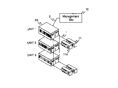
Figures I2A and 12B illustrate two of a variety of applications for
connecting test devices to a test access system 8 of the present invention. As
is
shown in Figure 12A, two connection lines may be established, namely, a test
line 1 established between a test device I 1 and a test access system 50, and
a
communication line 2 established between a test access system 50 and a
management site 12. The test line 1 enables the flow of signals between
communication lines connected to the test access systems 50 and the test
device
11. The communication line 2 enables the flow of control signals between the
test device 11 and the management site 12. As one can ascertain from Figure
12A, a number of test devices 11, I 1 a may be shared among several test
access
systems 50. That is, each test device 1 I, l la may be connected to more than
one
test access system 50. This is known as "bridging" the test devices I 1, l la.
For
example, and as is depicted in Figure 12A, test device 11 a is bridged with
Unit 1
on test equipment port 3, with Unit 2 on test equipment port 3, and with Unit
3
on test equipment port 3. Such a configuration enables a test device 11, l la
to
CA 02327284 2000-10-04
WO 99/53643 PCT/US98/27467
8
access a communication line connected to any of the connected test access
systems S0. Figure 128 shows a similar configuration of three modular test
access systems 50 connecting to a test device 11.
Figure 13 shows a number of test access units 50 serially connected to
other corresponding test access units SO via their communication ports 20.
Such
a setup allows a management device to communicate with a number of test
access units 50 through only one line. Such a feature is advantageous at sites
having limited availability to a network. That is, several daisy chained test
access units 50 at any one site may communicate with the remote management
device using only one modem. Each of the test access units 50 may be
configured by use of a unique unit address, setable using DIP switches on the
control card 25, to provide the management device with the identity of the
test
access unit 50 with which it is communicating. Thus, the test access units 50
connect with each other through their respective communication ports 20.
Connecting control lines to these ports 20 provide for communication among
these test access units 50, as well as with the system management device, such
as
a PCS. Preferably, a maximum of eight such test access units SO may be daisy
chained together.
Referring again to Figure 3, the control card 25 receives configuration
commands from a controlling device, such as a terminal or personal computer
via an RS-232 link or LAN connection provided through the communication
ports 20. The control card 25 may also provide outgoing information through
one of its communication ports 20, such as status information provided by the
control card 25. The use of the communication links make it particularly
efficient to perform remote testing.
The test equipment card 35 and line access cards 15 are internally
connected via three monitoring busses, MB1, MB2, and MB3, provided via a
motherboard. In a preferred embodiment; the motherboard also contains 9-pin
wire-wrap connectors which provide external connections to the communication
line circuits at the rear of the rack mount. The test equipment ports 30,
shown in
Figure 2, provides access to the test devices.
CA 02327284 2000-10-04
WO 99/53643 PCTNS98/27467
9
The test equipment card 35 provides test device access to three
monitoring busses, MB1, MB2, and MB3, simultaneously. Any three of the four
test ports, TP1-TP4, provided on test equipment card 35, can be connected to
any
of the three monitoring busses via a multiplexer (not shown). Each monitoring
bus is assigned to a group of five line access cards 15, as is shown in Figure
4A.
Only one port from a line access card 15 belonging to a certain monitoring bus
can be connected to that bus. Up to three ports, each one belonging to
different
monitoring busses, can be simultaneously connected to three of the test
equipment ports 30 on the test equipment card 35.
Preferably, the motherboard includes 90 9-pin wire-wrap connectors.
Eight of the pins of the wire-wrap connectors are used for connecting the
communication line circuits. The 9th pin of each wire-wrap connector is used
to
connect a tracer lamp. The tracer lamps, in the preferred embodiment, are
light
emitting diodes (LEDs) which are used to indicate the connectivity status of a
given communication line from a first termination (such as a first patch panel
at
the facility side) to a second termination (such as a second patch panel at
the
equipment side). The pin-out configuration of the 9-pin wire-wrap connectors
is
shown in Figure 4B. In addition, the motherboard contains fifteen 72-pin edge-
board female connectors for the line access cards 1 S, one 96-pin DIN male
connector for the test equipment card 35, and a 40-pin header connector for
the
test equipment interface 30. There are shorting MBB contacts between pins I-2,
3-4, 5-6, . . . , and 47-48 on the 72-pin edge board connectors, which provide
a
normal-through circuit on the communication line ports when line access cards
are not inserted.
Referring now to Figure SA, there is shown a block diagram of a line
access card 1 S in accordance with an embodiment of the present invention,
which provides a single patching capability for permitting cross connections,
switching, testing, and monitoring, including permanent and temporary
connections and terminations, respectively, to occur at a facility side 100 of
a
telecommunications network via transmit and receive lines, TXF 110 and RXF
120, respectively. Figure SB provides a front view of a line access card 15
CA 02327284 2000-10-04
WO 99/53643 PCTNS98/Z7467
incorporating a single patching capability. As is shown in Figure SB, line
access
card 15 includes jacks 144 to provide a user with manual and direct access to
six
communication lines or channels routed through line access card 15. Referring
to Figure SB, each of the facility jacks 144, which are shown vertically
aligned
as MON, OUT and 1N, respectively, correspond to a particular one of the six
communication lines (channels). The facility jacks 144 allow patching to the
facility side 100 of the test device.
As is illustrated in Figures SA-SB, line access card 15, which includes a
single patch circuit 140, is designed to operate within a test access system 8
by
10 providing a patch connection 140 which permits direct access to the
facility side
100 of the communication line circuit. The patch circuit 140 includes three
interfaces, namely, facility interface 130, switching circuit interface 136,
and
jack interface i44. The facility interface 130 is connected to equipment of
the
facility side 100 (RXF, TXF) of the network. The switching circuit interface
136
is internally connected to the switching circuit 150 of the line access card I
5.
The jack interface 144 includes three jack connectors located on the front of
the
line access card 15 labeled IN (input), OUT (output), and MON (monitor),
respectively. The IN jack provides access to the equipment to which the IN
jack
is terminated, and can be used to access or transmit signals into the
equipment
input. The OUT jack is used to monitor the output signals from the equipment
to
which the OUT jack is terminated. The MON jack serves a similar function as
the OUT jack by monitoring communication signals, but without breaking the
communication line circuit. In this manner, the MON jack allows for in-service
bridging of a digital line without interfering with line operation. In the
preferred
embodiment, the OUT jack observes the output signals from equipment to which
it is terminated by insertion of a patch cord into the OUT jack circuit.
As is also illustrated in Figure SB, line access card 15, which includes a
single patch circuit 140, further includes two groups of LED's 148, 152
located
on the front panel of line access card 15. The first group consists of six
bicolor
LED's 148 labeled "TEST/ALM". Each LED's 148 corresponds to a line access
port. In a "test" mode, the TEST/ALM LED's 148 illuminate a particular color
CA 02327284 2000-10-04
WO 99/53643 PCT/US98/27467
11
(e.g., green) to indicate whether a certain communication line port is being
tested
or not. In "alarm" mode, the TEST/ALM LED's 148 illuminate a second color
(e.g., amber) to indicate an alarm condition on a certain communication line
port.
The second group consists of six red LED's I52 labeled "TRACER" and
are used for identification of the cross-connections between different
communication line circuits. The TRACER LEDs 152 illuminate when a patch
cord is inserted into its corresponding jack; all other communication line
circuits
that cross-connect with the initial circuit also illuminate their
corresponding
tracer LEDs 152. This is accomplished by connecting the tracer pins on the
rear
of the test access unit 8 with the tracer pins of other units 8 via wire wrap
or
Telco pin (64 pin) connectors.
In accordance with one embodiment of the present invention, a line
access card 15, which includes a single patch circuit 140, comprises four
different printed circuit boards (PCB). A main PCB contains 48 nonlatching 2-
pole relays and six patch switches. One top mounted card contains relay
drivers,
control registers, status buffers, and decoders. Two front mounted LED cards
contain the LED's. One bottom mounted alarm card contains alarm circuits for
alarm and performance monitoring. In addition to the relay drivers, seven
control registers are utilized to effect the relays of the line access card 1
S by
initiating or terminating connections between sides of the communication line
ports and monitoring bus, as well as controlling illumination of the TEST/ALM
and TRACER LEDs 148, 152, a schematic representation of which is shown in
Figure 7.
Figure SC shows a layout of a line access card 1 S provided with a single
patch circuit capability. Referring to Figure SC, there is shown a line access
card
15 which includes three interfaces in accordance with an embodiment of the
present invention. A 56-finger edge-board connector 117 provides an interface
to a main motherboard. This interface 117 includes data bus, control signals,
and power supply lines. A 72-pin edge board connector 119 provides
connections to a communication line motherboard. This interface 119 includes
CA 02327284 2000-10-04
wo ~is~a3 PcTius9sma67
12
one monitoring bus and six communication line port connections. Six patch
connectors provide manual access to the facility side of the communication
line
circuits.
In an alternative embodiment, as is shown in Figures l0A and I OB, a line
access card 15 may comprise a dual patch capability comprising a patch circuit
140 associated with the facility side 100 of a telecommunications network, as
well as patch connection 180 connected directly to equipment side 200 of the
network. In accordance with this embodiment, line access card I S incorporates
dual patch circuits 140 and I 80 to permit line testing at a remote location
(i.e.,
customer premises of the communication lines incoming from an equipment
location). The group of line access cards 15 shown as LACB-LAC 1 S in Figure 1
illustrate line access cards incorporating a dual patch capability.
As previously stated, each patch circuit 140, 180 includes an equipment
interface 130, 131, a switching circuit interface 141, 181, and a jack
interface
144, 184, respectively. The equipment interface 130, 131 of each patch circuit
140, 180 is connected to the facility side 100 or equipment side 200of a
communication line circuit. The switching circuit interface 141, 181 of each
patch circuit 140, 180 is internally connected to the switching circuit 150 of
the
line access card 15. The jack interface 144, 184 of each patch circuit 140,
180
includes three jack connectors located on the front of the line access card
15.
The three jack connectors are labeled IN, OUT, and MON, respectively, and are
associated with either the equipment or facility sides 200, 100. Each IN jack
provides access to the equipment to which it is terminated. In particular,
each IN
jack can be used to transmit signals into the equipment (or facility) input.
The
OUT jack is used to monitor the output signals from the equipment to which it
is
terminated. The MON jack serves a similar function but without breaking the
circuit connection. The MON jack thus allows for in-service bridging of a
digital line without interfering with its operation. Temporary connections may
be made using patch cords between jack circuits, thereby permitting
restoration
of failed services or providing temporary connections for cut-overs.
CA 02327284 2000-10-04
WO 99/53643 PCT/US98/27467
13
As with a line access card having a single patch feature, a line access card
provided with a dual patching capability includes two groups of LED's 148, 152
located on the front panel of the line access card 15, as is best seen in
Figure
1 OB. The first group consists of six bicolor LED's 148 labeled "TEST/ALM".
Each of the LED's 148 corresponds to a line access port. In a "test" mode, the
TEST/ALM LED's 148 illuminate a particular color (e.g., green) to indicate
whether a certain communication line port is being tested or not. In an
"alarm"
mode, the TEST/ALM LED's 148 illuminate a second color (e.g., amber) to
indicate an alarm condition on a certain communication line port.
The second group consists of six red LED's 152 labeled "TRACER," and
used for identification of cross-connections established between different
communication line circuits. The TRACER LED's 152 illuminate when a patch
cord is inserted into its corresponding jack; all other communication line
circuits
that cross-connect with the initial communication line circuit also illuminate
their corresponding tracer LED's. This is accomplished by connecting the
tracer
pins on the rear of a test access 8 unit with the tracer pins of other test
access
units 8 via wire wrap or Telco pin (64 pin) connectors.
A line access card 1 S incorporating dual patch circuits 140, 180
comprises four different PCB's. The main PCB includes 48 nonlatching 2-pole
relays and twelve patch switches. One top mounted card contains relay drivers,
control registers, status buffers, and decoders. Two front mounted LED cards
contain the LED's. One bottom mounted alarm card contains alarm circuits for
alarm and performance monitoring.
Figure l OC shows the layout of a line access card 15 incorporating a dual
patching capability in accordance with an embodiment of the present invention.
Referring to Figure l OC, line access card 15 includes three interfaces. A 56-
finger edge-board connector 121 provides an interface to the main motherboard:
This interface 121 includes data bus, control signals, and power supply lines.
A
72-pin edge board connector 123 provides connections to the communication
line motherboard. This interface 123 includes one monitoring bus and six
communication line port connections. Twelve patch connectors provide manual
CA 02327284 2000-10-04
WO 99/53643 PCT/US98/27467
14
access to the equipment and facility sides 200, 100 of the communication line
circuits.
Referring now to Figure 6, there is shown a detailed block diagram of the
connections of a line access card I S which provides connectivity between a
selected communication line port selected through switch circuit I 50 of line
access card I 5 and a selected test device port (e.g., TP 1 - TP4). Figure 4C
provides a table of the various test access modes, and shows the
correspondence
between a selected mode of operation and the position of relays K1 through K18
shown in Figure 6. Figures 4D-4M are examples of selected test port
connections corresponding to each mode associated with a test access system
embodiment of the present invention.
When a communication line port is not being tested, the port operates in
a Transparent mode, i.e., the port is isolated from the monitoring bus and
there is
a normal-through path between "side E" and "side F" of the communication line
1 S port. Note that "side E" represents the equipment side 200 while "side F"
indicates the facility side 100 of a communication line circuit connection.
Data
flows through the circuit connection on the equipment side 200 and facility
side
100 without impediment from the test access system unit 8.
While operating in Transparent mode, the test equipment/access port is
either not connected or is placed in a loopback mode. When a test device port
is
not in use (i.e., isolated from the monitoring bus), it may be placed in a
loopback
mode. This allows a testing device to send out and receive back an idle code
while not testing. In a loopback AB mode of operation, data received from a
test
device is sent back to the test device. In particular, RXA on the test
equipment
port is connected to TXA on the same port. Any signals received on side A of
that port are returned to the test device. Similarly, RXB on the test
equipment
port is connected to TXB on the associated port. Any signals received on side
B
of the test port are returned to the test device. In a loopback A mode of
operation, data received on side A of the test equipment port is sent back to
the
test device, while in a loopback B mode of operation, data received on side B
of
the test equipment port is sent back to the test device.
CA 02327284 2000-10-04
WO 99/53643 PCTNS98/27467
In Mon EF mode there is also a normal-through path between sides E and
F of the communication line port. In addition, RXE and RXF of the
communication line port are connected to TXA and TXB of the test port. These
configurations provide for nonintrusive monitoring on both sides of a
communication line circuit. In a split EF mode of operation, sides E and F of
the communication line port are split and connected to sides A and B of the
test
port. In this mode, a test device is able to transmit and receive test
patterns
to/from both sides of the communication line circuits. In a Split AB mode of
operation, the communication line circuit is split and connected to the test
port in
10 a way that allows "drop and insert" testing to be performed by the testing
device.
Mon EFX, Split EFX, and Split ABX modes are similar, however, sides A and B
of the test port are swapped.
In addition to a line access card 15 of the present invention including
either single or dual patch connection capabilities, a line access card 15 may
also
15 include a performance monitoring feature 90, as is shown in Figures 8A-8C
and
9, which is capable of monitoring communication line circuits for variety of
line
anomalies and error information. Referring now to Figures 8A-8C, each line
access card I S is equipped with a monitoring function for collecting line
failures
from both the facility and equipment sides 100, 200 of six different
communication lines. Operation of the monitoring function in accordance with
an embodiment of the present invention is illustrated in Figure 9, while
Figures
8A, 8B, and 8C illustrate block diagram configurations for incorporation of
performance monitoring into no-patch, single patch, and dual patch circuit
embodiments, respectively.
Preferably, a performance monitoring function circuit 90 incorporated in
a line access card 15 of the present invention represents a high impedance
device, such that information signals passing through the line access card 15
are
not degraded. This feature is important to allow nonintrusive monitoring of
the
communication line. In one embodiment, line information is constantly
collected and stored in 15 minutes registers, 1 hour registers, and one day
registers. Performance monitoring occurs on each of the line access ports 91,
93
CA 02327284 2000-10-04
WO 99/53643 PCTNS98127467
16
simultaneously; that is, no multiplexing occurs in the preferred embodiment,
which allows the performance monitor feature to accept simultaneous real time
data from each of the associated lines (e.g., RXE, RXF). The information is
stored in the registers and can be retrieved at any time by the management
system 12. Once an alarm condition is detected, the CPU immediately sends an
alarm condition signal to the management system 12, which, upon reception,
presents it to the user. Each alarm event is presented to the management
software via the CPU with a time of day and date stamp. Register information
may be collected from the CPU at any time. If SNMP management software
with paging capability is used, the management software can page the user for
each alarm occurrence.
Performance parameters supported by the performance monitoring and
alarm functions of a test access system 8 of the present invention include
near-
end line performance parameters, and near-end path performance parameters and
alarms. Performance monitoring and alarm features are intended to monitor and
detect both line and path anomalies and defects. Line anomalies include a
bipolar violation (BPV), which occurs as a non-zero pulse of the same polarity
of
the previous pulse, and excessive zeros (EXZ), which includes any zero string
length greater than 7 contiguous zeroes (BBZS), as well as any zero string
length
greater than 15 contiguous zeroes (AMI).
Path anomalies include CRC-6 errors and frame bit errors (FE). CRC-6
errors are detected when a received CRC-6 code does not match the CRC-6 code
calculated from the received data. Frame bit errors are bit errors occurring
in the
received frame bit pattern. Line defects include loss of signal (LOS), while
path
defects comprise out-of frame (OOF), severely errored frame (SEF), and alarm
indication signals (AIS). Severely en:ored frames include the occurrence of
two
or more frame bit errors within a window. An AIS event indicates the
occurrence of an unframed signal having a "one's density" of at least 99.9%
present for at least three seconds. This is indicative of an upstream
transmission
interruption.
CA 02327284 2000-10-04
WO 99/53643 PCTNS98/27467
17
For near-end line failures, an LOS occurs when the LOS defect persists
for 2.5 seconds, t .5 second. Near-end path failures include and AIS and LOS,
while far-end path failures include a remote alarm indication (RAI), which
indicates a signal transmitted in the outgoing direction when equipment
S determines that it has lost the incoming signal. Other indicators include
the
near-end path failure count (count of near-end path failures) and far-end path
failure count. Near-end line performance parameters include code violation-
line
(CV-L), errored second line (ES-L), and severely errored second-line (SES-1).
Near-end path performance parameters include code violation-path (CV-P),
errored second path (ES-P), severely erred second-path (SES-P), SEF/AIS
second path (SAS-P), and unavailable second path {UAS-P). Alarms supported
include red alarm, blue alarm, yellow alarm, corresponding to loss of signal
(LOS), alarm indication signal (AIS) and remote alarm indication (RAI),
respectively.
Figure 9 shows a more detailed block diagram of the line access card and
performance monitoring and alarm functions associated with a test access
system
embodiment of the present invention. The alarm function is provided as an
attachment to the line access card 1 S, and provides performance monitoring on
both sides of a communication line circuit supported by the line access card
15.
Alarm card 127 includes 12 identical channels which monitor both sides (E and
F) of six communication line circuits. Each channel comprises an isolation and
impedance matching circuit (IIM) 131, receiver (RCV) 133, and framer (FR)
135. The isolation and impedance matching circuit 131 provides surge
protection, attenuation, isolation, and impedance matching required for
monitoring communication line circuit connections. Receiver 133 performs
data and timing recovery, and uses peak detection and variable thresholds for
reducing impulse noise. The framers 135 provide for alarm condition detection,
including:
Blue Alarm (AIS): when over a 3 ms window, five or less zeros are
received;
CA 02327284 2000-10-04
WO 99/53643 PCT/US98/Z7467
18
Yellow Alarm:
when bit 2 of 256 consecutive channels is set to zero for at least
254
occurrences;
or when the 12'" framing bit is set to one or two consecutive
occurrences;
or when I6 consecutive patterns of DOFF appear in the Facility
Data Link
(FDL);
Red Alarm (RCL): when 192 consecutive zeros are received.
In addition, the framers 135 include large counters for bipolar violations
(BPV),
line code violations (LCV), excessive zeros (EXZ), CRC-6 code violations, path
1 S code violations (PCV), frame bit error (FBE), and mufti-frame out of
synchronization (MOS) events.
It is noted that in the preferred embodiment, each receiver 133 is part of a
quad fully-integrated PCM receiver. As was previously mentioned, the receivers
133 perform data and timing recovery, and use peak detection and a variable
threshold to reduce impulse noise. The clock for receivers I 33 may be
provided
by an external 1.544 MHZ quartz crystal oscillator. Further, each framer 135
is
part of a quad fully-integrated framer. All four framers 135 are fully
independent. The receive side of each framer 135 performs alarm detection as
previously described.
Microcontroller 137 shown in Figure 9 is preferably a CMOS fully-static
8-bit device with 192 bytes of RAM and 22 I/O ports (such as Microchip
Technology P/N PIC16C63) having a synchronous serial port configured as a 3-
wire Serial Peripheral Interface (SPI) to communicate with the system CPU
(e.g.,
MC68302) via a system Serial Bus (SB). The Microcontroller 137 forms a local
8-bit multiplexed address/data bus 138 which is used for communication with
the framers 135. The clock for the Microcontroller 137 may be provided by an
external 3.6864 MHZ quartz crystal oscillator.
A test access system according to a further embodiment of the present
invention includes a software-based management and user interface coupled to
the CPU for remotely accessing and controlling the operation of the test
access
CA 02327284 2000-10-04
WO 99/53643 PCT/US98/27467
19
system. The management software permits a user who is located remotely from
the test access system 8 to execute a variety of functions, including mode
changes, diagnostic testing, and monitoring. The test access system 8 is
operable
to support several management options, including SNMP with Optional
Windows Based GUI (graphical user interface) Manager and TL 1. The SNMP
can be compiled into any SNMP compliant management software. Traps can be
set for the various alarms, and, upon detection, are sent to the SNMP
management software.
GUI application software then collects the alarm information in a
database, and provides reports and statistical graphs for a variety of alarms.
By
way of example, whenever an alarm message is received, the appropriate site
icon turns red, and an audio alarm sounds to alert the user monitoring the
terminal. Preferably, TL1 language is used for providing notification of alarm
events. However, other languages may be employed as necessary depending on
the particular application and requirements of the system.
A software interface receives signals from the CPU, such as CPU 98
shown in Figure 7, indicative of the status of a particular communication
line,
and displays such status to the user via the display screen of a user
interface 95.
Similarly, a user located at the display screen may initiate a change in
status or
perform a function, such as selection of a particular tracer LED at a console
remote from the test access system 8. Such a feature finds particular use when
attempting to identify a particular communication line among multiple rack
units. The particular line may be identified by blinking the tracer light
associated with that connection. The signal to initiate the blinking tracer is
sent
over the software interface to the device CPU 98 causing the appropriate
tracer
LED corresponding to the selected line access port to be illuminated. Such a
"manual" tracer feature, which allows a user at a remote location to directly
pulse a particular LED to indicate to a technician at the site of a particular
system
the location of a particular line for examination, is extremely advantageous
when
multiple lines and multiple patch panels co-exist in a common facility. This
manual tracer feature is provided in addition to the tracer feature activated
upon
CA 02327284 2000-10-04
WO 99/53643 PCT/US98/27467
insertion of a jack into a particular line access card 15. As one can
ascertain,
such remote access and monitoring significantly decreases the time necessary
for
a field operator to both diagnose and locate communication line connection
problems, as well as to test corrective actions.
5 Although preferred system embodiments of the present invention have
been disclosed for illustrative purposes, those skilled in the art will
appreciate
that many additions, modifications, and substitutions are possible without
departing from the scope of the present invention. For instance, a line access
card incorporating a single or dual patching capability, as well as the
10 performance monitoring feature, may also be incorporated into various other
test
access devices for T1-T4 transmission lines. Accordingly, all such variations
or
modification of the invention described hereinabove are intended to be
included
within the scope of the invention.