Note : Les descriptions sont présentées dans la langue officielle dans laquelle elles ont été soumises.
CA 02327331 2000-10-03
WO 99/52147 , PCT/US99/06879
DESCRIPTION
WIRE BOND ATTACHMENT OF A INTEGRATED CIRCUIT PACKAGE TO A
HEAT SINK
FIELD OF THE INVENTION:
The present invention pertains to the field of
integrated circuit packages and, in particular, to mounting
arrangements for securing an integrated circuit package to a
heat sink.
BACKGROUND:
Integrated circuits ("ICs") have many uses in
industries ranging from communications to consumer
IS electronics. By way of example, a power transistor IC is
formed by fabricating one or more transistor cells on a
silicon wafer, commonly referred to as a transistor "chip".
The transistor chip is attached to an insulating layer,
normally a ceramic substrate, which is thermally, but not
electrically, conductive. The ceramic substrate is itself
attached to a thermally conductive mounting flange. A
protective cover is secured to the flange, covering the
substrate and transistor chip, thereby forming a power
transistor IC "package."
Various electrically conductive (e. g., thin metal)
leads may be attached to, and extend away from the package,
in order to connect common terminals of the transistor chip
to other circuit elements located, e.g., on an adjacent
printed circuit ("PC") board. For example, with a bipolar
junction type power transistor, respective electrical leads
attached to the package are connected to a base, emitter and
collector of the transistor chip.
Because the power transistor package generates a
significant amount of heat during operation, the bottom
surface of the package mounting flange is normally directly
secured to a metallic heat sink underlying the PC board.
For example, a single layer PC board has a layer of
dielectric material between respective top and bottom
CA 02327331 2000-10-03
WO 99/52147 ~ PCT/US99/06879
2
conductive surfaces, wherein the bottom surface acts as a
reference ground. This bottom surface is connected, usually
with screws or solder, to the underlying metal heat sink, so
that the bottom surface and the heat sink have the same
ground potential with respect to any circuit elements
attached to the top surface of the PC board.
There are several known techniques for securing an IC
package to a heat sink surface. For example, as illustrated
in FIG. 1, an exemplary IC package 20 may be secured to a
heat sink 22 by a solder connection 28 between the bottom
surface of the package mounting flange 26 and the surface of
the heat sink 22.
While this approach is relatively simple, the solder
weld material 28 will invariably have a different thermal
expansion coefficient than the respective (typically metal)
mounting flange 26 and heat sink 22. As a result, the bond
between the mounting flange 26 and heat sink 22 will weaken
or even be destroyed by the thermal expansion stress between
the respective layers, especially when subjected to repeated
changes in temperature during each use of the IC package 20.
Further, the presence of the intervening bonding material
layer 28 may lesson the effectiveness of the heat conduction
between the flange 26 and heat sink 22. A still further
disadvantage with this approach is that, in order to remove
the IC package 20 for repair or replacement, the entire heat
sink 22 must be heated to break the solder bond 28, thereby
causing.any other solder bonds on the same heat sink 22 to
be weakened.
Referring to FIG. 2, as an alternative to using a
solder connection, the IC package 20 may be secured to the
heat sink 22 with a pair of screws 24 through openings
located on respective ends of the mounting flange 26.
Referring to FIGS. 3 and 4, still another technique for
securing an IC package to a heat sink is to insert one or
more screws 30 into, so as to be protruding above, the
surface of the heat sink 22. A resilient metal strip 32 is
extended from the screws) 30 and is shaped so as to apply a
' CA 02327331 2000-10-03
WO 99/52147 PCT/US99/06879
3
clamping force upon the cover of the IC package 20, thereby
distributing a substantially centered force that."secures"
the mounting flange 26 against the heat sink 22.
Still another method for securing an IC package to a
heat sink is disclosed and described in pending U.S. patent
application S/N 08/956,193, entitled, "Mounting Arrangement
For Securing An Integrated Circuit Package To A Heat Sink,"
which is fully incorporated herein by reference for all it
teaches. As taught therein, and as illustrated in FIG. 5, a
top surface 52 of a protective cover 50 of an IC component
package 40 is provided with a centered-protrusion 54. A
resilient retaining-spring~46 formed into a ribbon-like
shape having opposing ends 56 and 58 that extend from a
curvelinear bottom surface 60 is provided with an opening 62
IS sized to mate with the centered protrusion 54.
To mount the IC package 40 to a heat sink 42, the
retaining-spring opening 62 is compressively mated onto the
package cover protrusion 54 as the mounting flange 45 of the
IC package 40 is inserted between substantially parallel
walls 44 and 48 protruding from the heat sink 42, such that
the opposing retaining-spring ends 56 and 58 extend away
from the package cover 50 at substantially the same, albeit
reverse angles. The walls 44 and 48 are distanced from each
other just so as to cause moderate compression of the
opposing retaining-spring ends 56 and 58 toward each other
as the flange 45 is inserted against the heat sink 42.
The walls 44 and 48 are each provided with a respective
plurality of notches 64 and 68, which extend substantially
parallel to the heat sink 42 in a "ratchet-type" relief
pattern. Once the mounting flange 45 is pressed against the
heat sink 42, the opposing spring ends 56 and 58 are
retained in place by the respective wall notches 64 and 68.
In this manner, the spring 46 applies a retaining force
against the package cover 50, thereby securing the mounting
flange 45 against the heat sink 42, as indicated by the
arrow 70.
With any of the above-illustrated methods for securing
an IC package to a heat sink, once the IC package is secured
CA 02327331 2000-10-03
~WO 99/52147
PCT/US99/06879
4
to the heat sink, electrical leads extending from the
package (not shown in FIGS. 1-5) must be connected to
respective conductive surface leads or areas, e.g., located
on an adjacent PC board attached to the heat sink.
By way of illustration, referring to FIG. 6, the
mounting flange 86 of an IC package 80 is mounted on a heat
sink 82 via a conventional solder weld 84. A single layer
PC board 88 is also secured to the heat sink 82, e.g., by
screws (not shown) adjacent both sides of the package 80.
The PC board includes a metal top surface 90, a layer of
dielectric material 92, and a metal bottom surface 94,
respectively, wherein the bottom surface 94 and attached
heat sink 82 collectively act as a reference ground with
respect to circuit elements (not shown) attached to the top
surface of the PC board 88. Respective leads 96 and 98
extend from opposite sides of the package 80 and are
connected to corresponding conductive paths formed on the
top surface 90 of the PC board 88 via respective solder
welds 100 and 102.
As with the problems of using a solder weld connection
between the respective package flange (28) and heat sink
(22) described above in conjunction with FIG. 1, the solder
weld connections 100 and 102 are also prone to problems
caused by different thermal expansion coefficients between
the solder material, the conductive surface 90, and the
respective (metal) leads.96 and 98. In particular, the
solder material can crystallize after repeated heating and
cooling, causing welds 100 and 102 to weaken and/or fail,
with the respective leads 96 and 98 lifting and separating
from the surface 90 of the PC board 88.
Thus, it would be desirable to provide improved
arrangements for securing an IC component package to a heat
sink, whereby solder-welds are eliminated.
CA 02327331 2000-10-03
WO 99/52147 PCT/US99/06879
' S
SUMMARY OF THE INVENTION
The present invention provides improved arrangements
for securing an IC component package to a heat sink in a
manner which provides for the non-solder-based connection of
leads extending from the package to respective conductive
pathways located on an adjacent PC board surface.
In a preferred embodiment, a thermally conductive
mounting flange of an IC package is placed directly on a
heat sink surface between respective sections of single
layer PC board attached to the heat sink, such that
electrical leads extending from opposing sides of the
package are positioned over corresponding conductive areas
formed on the surface of the respective adjacent PC board
section. In accordance with a first aspect of the
IS invention, the respective package leads are each connected
to the corresponding PC board areas by one or more flexible
bond wires. In addition to electrically connecting the
package leads to the respective PC board sections, the bond
wires collectively secure the package to the heat sink in a
manner allowing for lateral movement between the respective
flange and heat sink surfaces in response to thermal
stresses.
As will be apparent to those skilled in the art, other
and further objects and advantages will appear hereinafter.
BRIEF DESCRIPTION OF THE DRAWINGS
The~drawings illustrate both the design and utility of
the present invention, in which similar elements in
different embodiments are referred to by the same reference
numbers for purposes of ease in illustration, in which:
FIG. 1 is a side view of a first prior art mounting
arrangement, wherein an IC package is soldered or otherwise
bonded to a heat sink;
FIG. 2 is a partial cut-away side view of a second
3~ prior art mounting arrangement, wherein mounting screws are
employed for directly attaching an IC package to a heat
sink;
CA 02327331 2000-10-03
wo 99/si~a~
PCT/US99/06879
6
FIG. 3 is a side view of a third prior art mounting
arrangement, wherein a single retaining screw and retaining
strip extending therefrom are used to secure an IC package
to a heat sink;
FIG. 4 is an side view of a fourth prior art mounting
arrangement, wherein a pair of retaining screws and a
retaining strip extended therebetween are used to secure an
IC package to a heat sink;
FIG. 5 is a partial cut-away side view of a still
further arrangement for mounting an IC package to a heat
sink, wherein a resilient, ribbon-shaped retaining-spring is
affixed to the center of a~protective cover of the package
and held in place by a pair of opposing walls protruding
from the heat sink;
FIG. 6 is a partial cut-away side view of an IC package
solder bonded to a heat sink, whereby conductive surface
leads on an adjacent PC board are connected to respective
leads extending from the package via a prior art solder weld
connections;
FIG. 7 is a top view of a preferred power transistor
package attached to a heat sink by a plurality of flexible
bond wires connecting respective leads extending from the
package to conductive areas formed on adjacent PC board
sections attached to the heat sink; and
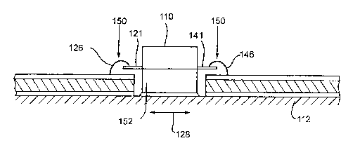
FIG. 8 is a partial cut-away side view of the
arrangement of FIG. 7.
DETAILED DESCRIPTION OF THE PREFERRED EMBODIMENTS
Referring to FIG. 7, a power transistor package 110 is
positioned on a heat sink 112 between first and second
sections 113 and 114 of single layer PC board attached to
the heat sink 112. The transistor package 110 includes a
first plurality of leads 117, 119 and 121 attached to one
side 130, and a second plurality of leads 137, 139 and 141
attached to an opposite side 132. In particular, the
package 110 is positioned on the heat sink 112 such that the
electrical leads 117, 119 and 121 on the first side 130
CA 02327331 2000-10-03
WO 99/52147 PCT/US99/06879
7
extend over corresponding conductive areas 116, 118 and 120
formed on the surface of the first PC board section 113, and
the electrical leads 137, 139 and 141 on the opposite side
132 extend over corresponding conductive areas 136, 138 and
140 formed on the surface of the second PC board section
114, respectively.
In a preferred embodiment, the conductive areas 116,
118, 120, 136, 138 and 140 are formed by selectively
removing a portion of the conductive (i.e., metallic) top
surface of the respective first and second PC board sections
113 and 114 to thereby expose the underlying dielectric
material 115. The exposed areas of dielectric material 115
act as a non-conductive boundaries defining the respective
conductive areas 116, 118, 120, 136, 138 and 140.
The transistor package leads 117, 119, 121, 137, 139
and 141.are connected to the corresponding conductive PC
board areas 116, 118, 120, 136, 138 and 140 by respective
pluralities of resilient, conductive bond wires 122, 124,
126, 142, 144 and 146. The bond wires 122, 124, 126, 142,
144 and 146, which are preferably made of suitable material,
such as aluminum, gold or an aluminum alloy, electrically
couple the package leads 117, 119, 121, 137, 139 and 141 to
the respective conductive PC board areas 116, 118, 120, 136,
138 and 140, while collectively securing the package 110 to
the heat sink 112.
More particularly, the respective pluralities of bond
wires 122, 124, 126, 142, 144 and 146 are bonded on one end
to the respective conductive PC board areas 116, 118, 120,
136, 138 and 140, and at the other end to the respective
package leads 117, 119, 121, 137, 139 and 141. The
individual bond wires are preferably attached to the
respective conductive areas and package leads via
conventional means, such as, known ultrasonic wire bonding
techniques.
As best seen in FIG. 8. the rP~i 1 ian~-A of tl,o ...
provides a force against the respective package leads in the
direction indicated by the arrows 150, thereby pressing a
mounting flange 152 underlying the transistor package 110
CA 02327331 2000-10-03
VNO 99/52147
PC'T/US99/06879
8
flush against the heat sink 112. Because the package flange
152 is not affixed in place, the illustrated mounting
configuration allows for the package 110 to move laterally
relative to the heat sink 112, as indicated by the arrows
128, to avoid any thermal stresses that may otherwise
result. Further, at least one advantage of employing bond
wires to connect the package leads 117, 119, 121, 137, 139
and 141 to the respective conductive PC board areas 116,
118, 120, 136, 138 and 140 is that solder connections are
not needed.
Thus, preferred embodiments have been disclosed of an
improved mounting arrangement for securing a IC package to a
heat sink. While embodiments and applications of this
invention have been shown and described, as would be
apparent to those skilled in the art, many more
modifications and applications are possible without
departing from the inventive concepts herein.
The scope of the invention, therefore, are not to be
restricted except in the spirit of the appended claims.