Note : Les descriptions sont présentées dans la langue officielle dans laquelle elles ont été soumises.
CA 02328624 2000-10-12
WO 99!54679 PCT/US99/08721
NON-DESTRUCTIVE ANALYSIS OF A SEMICONDUCTOR USING
REFLECTANCE SPECTROMETRY
CROSS-REFERENCES TO RELATED APPLICATIONS
This application claims the benefit of U.S. Provisional Application No.
60/082,639 filed Aprii 21,1998, the disclosure of which is incorporated by
reference.
FIELD OF THE INVENTION
This invention relates generally to the field of semiconductor metrology,
and more particularly, to the use of infrared spectrometry to non-
destructively determine
depth profiles of doped semiconductors.
BACKGROUND OF THE INVENTION
The ability to non-destructively measure the thickness and dopant profiles
in semiconductors has long been sought by the integrated circuit (IC)
industry. In fact,
dopant profile measurement techniques have been a subject of investigation for
over 30
years. In one technique, referred to as Secondary Ion Mass Spectroscopy
(SIMS), the
dopant profile of a semiconductor is measured as it is incrementally destroyed
layer by
layer. As a result, a dopant profile is obtained, however, the semiconductor
material is
lost.
It is common knowledge in solid state physics that the introduction of
dopants into a semiconductor alters its optical properties in the infrared
spectral range due
to the presence of free carriers. At the simplest conceptual level, free
carriers contribute
to the optical constants n and k as described by the well known Drude model.
Thus far,
optical measurement techniques can be classified into two categories, namely,
the
Infrared Reflectance (IR) technique and the Fourier Transform Infrared (FT-IR)
Interferometry technique.
CA 02328624 2000-10-12
WO 99/54679 PCT/US99/08721
2
Infrared Reflectance fIR) Technique
The IR technique was first used in 1960 to measure the thickness of silicon
epitaxiaI (epi) layers. The technique exploits the existence of optical
contrast in the
infrared spectrum due to different doping levels in a lightly doped epi-layer
and a heavily
doped substrate. The different doping levels cause interference when IR light
is reflected
from the surface of the sample. For an epi-layer exceeding 2 micrometers (um)
in
thickness, the reflectance waveform produces oscillatory behavior allowing the
film
thickness to be derived from the distance between the adjacent interference
fringes. The
technique has a number of disadvantages, the main one of which is that the
position of the
interference fringes is strongly influenced by the substrate dopant
concentration, as well
as the disappearance of the fringes altogether for sub-1 um epi-layers. There
have been
attempts to improve the technique by accounting for the phase changes upon the
reflection at the epi/substrate interface. One theory calculated such changes
using
classical Boltzmann statistics, however the computations failed to agree with
experimental results across the broad IR frequency range of 5-40 um. The
computations
also failed to agree with experimental results wherein the phase shift
correction is
particularly significant for thin epi-layers. Attempts have also been made to
extend the
IR reflectance technique to thin (0.5 um) epi-layers by comparing the Drude
model with
other known models. It was found that the Drude model is more applicable to
epi-layers
on heavily doped substrates, such as 2E 19 cm 3, while other models are more
accurate for
lightly doped substrates, such as SE18 cm 3. No model was able to adequately
describe
both cases. Currently, the IR technique is only applicable to the measurements
of epi-
layers thicker than 2 um with substrate resistivity less than 0.02 S2-cm and
epi-layer
resistivity less than 0.1 i2-cm.
~25 Fourier Transform Infrared (FT-IR) Interferometry Technique
The FT-IR technique has found wide-spread use as a powerful tool for
chemical analysis of materials where various material properties can be
inferred from
their infrared absorbance spectra. The application of FT-IR for film thickness
determination was introduced in 1972 for measurements of thin polymer films
and has
since been widely adopted by the IC industry as the standard method for epi-
layer
thickness measurements. Unlike the IR technique, which uses dispersive
infrared
spectrophotometry, this method uses FT-IR in an interferogram mode. An
instrument
CA 02328624 2000-10-12
WO 99/54679 PC1'/US99/08'121
implementing an FT-IR consists of a Michelson interferometer coupled to a
computer _
system. A Michelson interferometer divides a beam of radiation from an
incoherent
infrared source into two paths and recombines them at a detector after a path
difference
has been introduced, creating a condition under which an interference between
the two
beams can occur. The intensity variation as a function of the path difference
is captured
by the detector and results in the interferogram.
A typical interferogram consists of a strong center burst and two similar
smaller bursts positioned symmetrically to the sides of the center burst. The
epi-layer
thickness is determined according to the formula:
__ a ()
d 2n cos 0 1
where d is the epi-layer thickness, 2O is the distance between the side-bursts
in the
interferograms (same as the path difference between the two beams), n is the
refractive
index of the epi-layer, and 6 is the angle of refraction in the epi-layer.
However, as the
film thickness decreases, the side-bursts move into the strong center burst
until they get
completely obscured, making the epi-layer measurement by side-burst
identification
impossible. This occurs when the epi-layer thickness is reduced below
approximately 1
um. Attempts at extending the interferogram measurements to thinner films by
utilizing a
center-burst cancellation technique, wherein an interferogram of a matched
substrate is
subtracted from the initial measurement, have produced very limited success.
Even if a
perfectly matched substrate could be found, this still does not account for
the secondary
contribution to the center-burst formation due to the epi-layer presence, nor
are the
frequency responses of the instrument's optical and electronic components and
the
material properties taken into consideration. These items create phase shifts
in the
interferogram which influence the shape and absolute and relative positions of
the side-
bursts. Even in the cases where the film thickness is sufficient for side-
burst
identification, these phase shifts cause enough of an error to make film
thickness
measurements approaching 1 um increasingly uncertain.
In view of the above, what is needed is an improved technique to obtain an
accurate non-destructive measurement of film thickness or dopant
concentrations of
doped semiconductors. This includes such semiconductor structures as silicon
epitaxial
layers on silicon substrates where the epi-layer has a different doping level
from the
substrate, for example, an undoped or lightly doped epi-layer on a heavily
doped
CA 02328624 2000-10-12
WO 99/54679 PCT/US99/0$721
4
substrate. The technique should also work for structures having an ion-
implanted or
diffused profile, where a layer of dopants is introduced into a semiconductor
having a
lighter dopant level, including such specific structures as buried layers and
shallow
junctions. In both of these examples, the improved technique should enable one
to
determine the thickness of the epitaxial or implanted layer, the thickness of
the transition
layer between the film and substrate, and the concentration of free Garners in
the film and
the substrate, without having to destroy the sample in the process. In
addition, the
technique should account for imperfections in the measuring device and yield
accurate
results for sub-1 micron epi-layers.
SUMMARY OF THE INVENTION
The method and apparatus of the present invention provides an improved
technique for non-destructively measuring sub-1 micron dopant profiles in a
semiconductor. The invention enables one to determine the thickness of an
epitaxial or
implanted layer, the thickness of a transition layer between the film and a
substrate, and
the concentration of free carriers in the film and the substrate, without
having to destroy
the sample in the process. In addition, the method is applicable to any
semiconductor
structure where an optical contrast exists in the 1R range, for example 50 to
7000
wavenumbers, due to the presence of free carriers created by the introduction
of dopants.
The invention is suitable for layers as thick as tens of microns and as thin
as several
angstroms (~ = 1 E-8 cm), and detects dopant concentrations as low as several
E 16 cm 3.
The method also corrects for instrument imperfections thereby yielding more
accurate
results.
In a first embodiment of the invention, a method is provided for
determining at least one parameter of a semiconductor. The method starts by
measuring
an experimental reflectance spectrum of the semiconductor. An analytical model
of the
semiconductor is constructed having a film layer, a transition layer and a
substrate layer.
Next, optical constants n; and k~ for the film layer, transition layer and
substrate layer are
expressed as a function of doping level. A profile of the transition layer is
determined,
and if an abrupt profile exists, the transition layer is not included in the
semiconductor
model. If a graded profile exists, the transition layer is further modeled as
having a
plurality of sections, wherein each of the sections is assigned an s-
polarization matrix and
a p-polarization matrix. An overall modeled reflectance spectrum is then
calculated and
CA 02328624 2000-10-12
WO 99/54679 PCT/US99/08721
the parameters therein are varied to achieve a best fit relationship with tine
experimental .
reflectance spectrum. Thus, the parameter of interest can be determined.
In a second embodiment of the invention, the method of the first
embodiment is modified wherein a polarizer is used so that the experimental
reflectance
5 spectrum is derived from radiation of a known polarization. This reduces the
effects of
instrument imperfections on the experimental data and results in simplifying
the overall
reflectance model. The parameter of interest is then obtained in the same
manner as in
the first embodiment.
In a third embodiment of the invention, a method is provided wherein two
polarizers and an achromatic retarder are used to obtain an experimental
reflectance
spectrum expressed as a function of amplitude and phase. An overall modeled
reflectance
spectrum is calculated as done in the first embodiment, however, additional
computational steps are taken to express the modeled reflectance spectrum as a
modeled
amplitude and a modeled phase. The parameters of the modeled amplitude and
modeled
phase are varied to achieve a best fit with the experimental data, thereby
determining the
desired parameter.
BRIEF DESCRIPTION OF THE DRAWINGS
FIG. 1 shows an embodiment of the present invention;
FIG. 2 shows a method of the present invention for use with the
embodiment of FIG. 1;
FIG. 3 shows a multi-stack model of a semiconductor sample;
FIG. 4 shows a model of a transition layer;
FIG. 5 shows results of the method of FIG. 2;
_25 FIG. 6 shows results of a SIMS measurement;
FIG. 7 shows another embodiment of the present invention;
FIG. 8 shows another embodiment of the present invention;
FIG. 9 shows another method of the present invention for use with the
embodiment of FIG. 8;
FIG. 10 shows a detailed diagram of the embodiment of FIG. 8;
FIG. 11 shows a graph of ~Xp for samples of various epi-layer thickness;
and
FIG. 12 shows a graph of DeXp and Omoa for a 0.2 um epi-layer sample.
CA 02328624 2000-10-12
WO 99/54679 PCT/US99/08721
6
DESCRIPTION OF THE SPECIFIC EMBODIMENTS
In several embodiments of the present invention, a procedure is defined
wherein an experimental reflectance (IteXp) measurement is collected using an
apparatus
constructed according to the teachings of the present invention. A
comprehensive
parameterized analytical model reflectance (R~) is created containing
parameters which
model the residual instrument imperfections as well as quantities of interest,
such as film
thickness, dopant concentration and other quantities of interest. The Rmoa is
derived from
quantum physics and results in several improvements over the Drude model. For
example, the R",od of the present invention provides better accuracy for
characterizing
small films. Additionally, the R~"od is accurate over a wide range,
approximately 200-
6000 wavenumbers, and allows the use of more of the measured infrared
radiation. This
is particularly important at the low end of the spectrum, namely 200-1000
wavenumbers,
where there is generally high optical contrast between the film and the
substrate. Further,
1 S the Rm~ provides more accurate results when using substrates having low
dopant
concentrations. Once the Rmoa is created, a determination of the parameters is
achieved
by optimizing the R,"od for the best possible fit to the experimental
measurement R~XP.
FIG. 1 shows an embodiment of the present invention depicting a
measurement apparatus 100. The measurement apparatus 100 comprises an FT-IR
spectrometer which includes a computer 102, a radiation source 104, optics
106, a
specimen holder 108 and a detector 110. When a specimen of interest is placed
in the
specimen holder 108, a measurement may be taken when the computer 102 commands
the source 104 to emit source radiation l OS into the optics 106. The source
radiation is
partially coherent infi~ared radiation in the range of 200-6000 wavenumbers.
The optics
2S 106 redirects at least part of the source radiation to form an incident
beam 112 directed
towards the specimen in the specimen holder 108. A reflected beam 114 is
formed when
at least a portion of the incident beam 112 reflects off the specimen in the
specimen
holder 108. The detector I 10 detects information from the reflected beam 114
and inputs
the information to the computer 102. The computer 102 then performs various
processing
functions on the detected information allowing analysis of the specimen.
Included as part of the measurement apparatus 100 is a reference sample
116. The reference sample 116 comprises either a highly reflecting gold mirror
or a
highly polished silicon wafer having a high doping level, such as 1 E 19 crn
3. The
CA 02328624 2000-10-12
WO 99/54679 PCT/US99/08721
7
reference sample can be used to obtain ideal measurements which may be used
for
comparison or analysis of the measurements taken from the specimen of
interest.
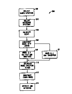
FIG. 2 shows a flow chart for a measurement method 200.for non-
destructively measuring the doping levels of a semiconductor material. The
measurement
method 200 comprises a number of steps wherein measurements of a specimen of
semiconductor material and measurements of the reference i 16 are analyzed.
In step 202 an infrared spectrum of the semiconductor material (IS~,p) is
taken. The semiconductor material is placed in the specimen holder 108 and the
infrared
spectrum consists of a measurement of the spectral intensity of the reflected
beam 114 as
a function of the wavenumber of the source radiation 105.
In step 204 the reference. sample is placed in the specimen holder and an
infrared spectrum of the reference sample (Iref) is taken. The reference
sample may be
either the gold minor or the highly polished silicon wafer.
In step 206 an experimental reflectance R(exp) is obtained according to the
following equation:
R(exp) . Lamp (2)
Iref
In step 208 an analytical model of the semiconductor is constructed. The
analytical model models the refractive properties of the semiconductor and
contains
parameters which represent quantities of interests, such as the thickness of a
film layer.
FIG. 3 show a mufti-stack analytical model 300 of the semiconductor
constructed according to the teachings of the present invention. The mufti-
stack model
300 includes a layer of native oxide Si02 302 having a thickness do, a film
layer 304
having a doping level N~ and having a thickness d1, a transition layer 306
having a
thickness due" wherein a doping level having a depth profile exists and a
substrate 308
having a doping level N2. Although the model 300 is shown with only one film
layer
304, it will be apparent to one with skill in the art that the model 300 may
contain more
than one film layer and that such additional layers could be modeled in a
similar fashion
to film layer 304.
CA 02328624 2000-10-12
WO 99/54679 PCT/US99/08721
Referring again to step 208, best guess initial values are assigned to the
doping levels N1, N2 and the thickness values due", do and dl by the user. In
addition, a
doping profile of the transition layer 306 is modeled by a parameterized
function A(X~,
Xz), where initial values are assigned to the parameters Xi and Xz by the user
based on
generally known transition layer profiles. The initial values of the
parameters form only a
starting point from which more exact values will ultimately be determined.
Steps 210 and 211 define two respective representations of the refractive
properties of the mufti-stack model. The user determines which representation
to
construct based on whether the user desires the transition layer to have an
abrupt profile
or a graded profile. If the abrupt profile is selected, then the
representation of step 210 is
constructed wherein the transition layer is not included. If the graded
profile is selected,
then the representation of step 211 is constructed wherein the transition
layer is included.
In the following methods, the SiOz layer is not considered, since this layer
is generally
very thin and has relatively simple optical properties. However, it will be
obvious to
those of skill in the art that the Si02 layer can be easily included in the
methods of the
present invention without deviating from the scope of the invention.
In step 210, complex indices of refraction ni are constructed. Each n;
corresponds to a layer in the multistack model 300 of FIG. 3 and comprises a
pair of
optical constants n; and k; according to the expression:
n. = n. +jk~
In this step the user has defined the transition layer as having an abrupt
profile, and as a result, the transition layer will not have an associated ni.
Thus, nI will be
constructed only for the film layer 304 and the substrate 308. In a way
distinct from the
Drude model, equations derived from quantum physics are used to define the
optical
constants n; and k, associated with each ni. By using this technique several
advantages
over the Drude model are derived. First, ni may be accurately defined for
thinner films.
Second, ni may be accurately defined for a greater radiation range, for
example 250-6000
wavenumbers. Third, the technique is accurate when using substrates having
lower
dopant concentrations. Thus, with the above advantages, n; and k; are
described as a
CA 02328624 2000-10-12
01/18%OC l.?:28 FA.g 41.5 578 OJOC TOWNSEND 5F
-- .- __.- ..- . ._ _.-. _.~.._._.-_-._- --_--_ ... .... -.,.._._-
>s ~~~ ..
~~AIIJS 1$ JAI Z~~Q
9
function of the doping level in the corresponding regions according to the
following
equations:
n~z=2( ~z+~"z+s) and k;z=2( s~+~"z-e) (3)
where;
3kT ~~g(E) 1 + rvz zz Ivlz ~~ (1 f~
and;
3kT ~~g(E)1+~ZZZ ~'Izfp(1-fp)
where;
to w~2(~7 = m" E (~
S~E) =1 / 2tcz (2m' / ~tz)'n Emz
z
1 Zze'N; 4sraE ( )
i(E) a 16~r(2m~)~m~,zEmz ~ 1+ 7ezN,m3
1 9
fo = 1 + e'~-~f "'~ ( )
and Efis determined from the following constraint;
?o Ne = Jfog~>~ (
where N; is the doping level in the corresponding region, v is the velocity of
fret
carriers, T is the free carrier scattering time and wherein N~, z aad a are
determined
recursively.
CA 02328624 2000-10-12
WO 99/54679 PCT/US99/08721
Once the pair of optical constants n; and k; for each of the film layer and .
the substrate have been calculated, a perpendicular reflectance (Rs) and a
parallel
reflectance (Rp) can be calculated according to the following equations.
Rf = rsrs» (11)
5 Rp = rprp~ (1 la)
where;
_ rOlp + rl2pe-'z~
rP 1 + rOlprl2pe-'z~ (12)
rOls + rl2se-'z~
r5 = 13
1 + rOlsrl2se''z~ ( )
nl cos cp0 - n0 cos cpI ( )
rOlp = nlcoscp0+nOcoscpl 14
nl cos cp0 - n0 cos cp2 )
r12 p = nl cos cp0 + n0 cos cp2 (1 S
r01 s = nl cos cp0 - n0 cos cpl ( 16)
nl cos cp0 + n0 cos cpl
rl2s- nlcosc~0-nOcoscp2 (1~)
nl cos cp0 + n0 cos cp2
(3 =2n(~)(nlz -nOz sinz cpp)~~z (18)
and ni are the respective complex indices of refraction in the corresponding
material layer. For example, n0, nl, and n2 correspond to the complex
refractive indices
of the air, the film, and the substrate, respectively. For example, the index
for the air is
simply 1, the index of the film is typically 3.42 and the index of the
substrate is derived
depending on the Garner concentration according the quantum physics of Eqs.(3 -
10).
The angles cp0, cp 1, cp2 refer to the complex angles of propagation of light
in the air, the
CA 02328624 2000-10-12
WO 99/54679 PCT/US99/0$721
11
film and the substrate respectively. In calculating these angles, cp0 is
typically 30 degrees,
but may be varied, while cp 1 and cp2 are determined through Snell's law from
the
expressions:
n0*sin(cp0) = nl*sin(cpl) (18a)
and
n0*sin(cp0) = n2*sin(cp2) (18b)
In step 211 the user may select to represent the transition layer as having
the graded profile. A transition layer reflectance model is created wherein
the shape and
thickness of the transition layer can then be determined.
Fig. 4 shows the transition layer reflectance model 400 used to model the
transition layer 306. The model 400 represents the transition layer divided
into a number
of sections 402. The precise number of sections is determined by the user.
Defining
more section may yield more accurate results but may increase processing time.
Defining
fewer sections may yield less accurate results but may decrease processing
time. Each
section is assigned a transition characteristic matrix M, which fox s-
polarization is given
by:
M = cos 8 - p sin 8 ( 19)
5
-ipsin8 cos8
and for p-polarization is given by;
cos ~ - 1 sin 8
MP = q (20)
- iq sin ~ cos ~
where;
8 = 2~a(n;coscp;)t
p =n; coscp; = n;z -(no sin6a)Z '(21)
CA 02328624 2000-10-12
WO 99/54679 PCT/US99/08721
12
cos cp;
q-
n;
In the above equations, a is the wavenumber in cm ~, A is a complex angle
of propagation in the section, t is the thicla~ess of the section, np is the
refractive index in
air, cpo is the angle of incidence in air (typically 30°) and ni is the
complex index of
refraction of the corresponding section defined by the quantum physics of Eqs.
(3-10).
The equations (18a) and (18b) are used to determine cpi from cpo.
The overall transition characteristic matrices for the transition layer is
given by the product of the individual matrices of each section, where n is
the section
number, as:
Mslp -llMr = tli, tliz (22)
tl.,; t122 sIv
Utilizing the same technique, a characteristic matrix for the filin layer can
be defined as:
fll f12
(22a)
Mfs, p = f21 f 22
Thus, the overall characteristic matrices for the total model is given by the
product of the film matrices and the transition matrices expressed as:
mll m12
Mtots,p = MS,p * Mfsip = (22b)
m21 m22
In the above step it is possible to factor in the contribution of the SiOz
layer by forming its characteristic matrix utilizing the same technique and
multiplying it
with the film and transition layer characteristic matrices of Eq. 22b.
Based on the total characteristic matrices the reflection coefficients from
the sample for s-polarization are given by;
CA 02328624 2000-10-12
WO 99/54679 PCT/US99/08721
13
r = (m~ Wf' m~zPs )Po - (mz~ + mzzPs ) (23)
s
(my' m~zPs )Po '~' (mzW' mzzPs )
and the reflection coefficients from the sample forp-polarization are given
by;
r - (m" +mmQs)qo -(m~, +mzz9s) (24)
(m» +m~zqs)qo +(mz~ +m=z9s)
with po and ps for the incident medium (air) and substrate, respectively,
therein accounting for the effects of the substrate on the reflection
coefficients.
The s and p polarized reflectances for the case of the transition layer
having a graded profile are given by:
Rs - rs rs (25)
Rp = rp rp* (25a)
Referring again to Fig. 2, in step 212 an overall reflectance for the model
(Rmo~ is obtained according to the selected transition layer modeling. If the
abrupt
profile was selected by the user then RS and Rp from equations (11) and (1 la)
are used. If
the graded profile was selected, then RS and Rp from equations (25) and (25a)
are used.
As a result, the overall reflectance model can be expressed according to the
following
equation:
Rmod - Rs~(a~~) + Rp~(a~~) (26)
where ~ and ~ are the frequency dependent parameterized functions
containing polarization properties of the FT-IR instrument with the parameters
a and (3 to
be determined during an upcoming step.
In step 214 an error function {MSE) is created and expressed as:
CA 02328624 2000-10-12
WO 99/54679 PCT/US99/08721
14
MSE = ~ [Rexp - Rmod (z)]Z (27)
k
where Rmod(z) is the modeled reflectance spectrum of equation (26) and
the quantity z is the vector of parameter values: z = [Nl, N2, do, d1, due",
X~, Xz, a, (3].
In step 216 an optimization and determination process is performed. To
accomplish the optimization, the parameter vector z is varied according to a
non-linear
regression procedure, such as in the Levenberg-Marquart non-linear regression
method,
so as to minimize the MSE. Once the MSE is minimized, the corresponding vector
z
contains the parameters of interest, such as the thickness of the film layer.
FIG. 5 shows an example of Rexp and Rmod values for a 0.2 um epi-layer
sample with an associated substrate layer. Graph 500 shows reflectance values
versus
wavenumbers wherein the Rexp values are plotted as a solid line and the Rmod
values are
plotted as a dotted line. The optimization step 216 in the measurement method
200
determined that for the known 0.2 um epi-Iayer sample, the thickness of the
epi-layer was
245.3 nm and the substrate doping level was 6.12E19 cm 3.
FIG. 6 shows the results obtained when the same sample was measured
using Secondary Ion Mass Spectroscopy (SIMS). SIMS is a destructive
measurement
technique wherein the sample is destroyed layer by layer as the measurements
are taken.
As can be seen at point 602, the depth of the epi-layer was approximately 240-
250 nm.
The substrate dopant concentration is shown at 604 and was approximately
6.1E19 cm 3.
Thus, the two methods obtained approximately the same result while the
measurement
method 200 of the present invention did not destroy the sample as required by
the SIMS
technique.
Fig. 7 shows another embodiment of the present invention comprising a
measurement apparatus 700 constructed according to the teachings of the
present
invention. The measurement apparatus 700 comprises the FT-IR spectrometer of
FIG. 1
which includes the computer 102, source 104, optics 106, specimen holder I08
and the
detector 110. The measurement apparatus 700 also includes the reference sample
116.
Aiso included in the measurement apparatus 700 is an adjustable infrared
polarizes 702.
The adjustable infrared polarizes 702 is positioned between the optics 106 and
the
specimen holder 108, so it is in the path of the incident beam 112. The
adjustable
infrared polarizes 702 is used to set the state of polarization of the
incident beam 112 to a
CA 02328624 2000-10-12
WO 99/54679 PGT/US99/08721
selected value. Usually the selected value is either full s-polarization or
full p- .
polarization, but maybe any combination of s and p polarization as desired. By
setting
the polarization of the incident beam 112, the effects of imperfections in the
measurement
apparatus 700 are eliminated, since the ratio of s and p polarization of the
incident beam
S can be accurately set to lalown values. This serves to reduce the number of
parameters in
the optimization vector z by eliminating the parameters a and ~3,
thereby'increasing the
robustness and accuracy of the measurements.
The measurement method 200 can be used with the measurement
apparatus 700, however, the adjustable infrared polarizes 702 results in a
simplification or
10 variation in steps of the measurement method 200 as described below.
In the step 212 the value Rmod in Eq. (26) is given by either Rs or Rp
according to the polarization setting of the adjustable infrared polarizes
702. Thus, the
parameters a and (3 are removed from the optimization vector z as a result of
using the
adjustable infrared polarizes 702. For example, if the adjustable infrared
polarizes 702 is
15 set for full s-polarization, the Rmod value is given by:
Rmod = Rs
If the adjustable infrared polarizes 702 is set for full p-polarization then
the
Rmod value is given by:
Rmod = Rp
The values of R$ and Rp are determined as in the first embodiment wherein
the user selects the profile of the transition layer and models the optical
constants in either
step 210 or step 211 accordingly.
The step 2I4 is performed as before, however, in the error function (MSE),
Rmod(z) is simplified and fewer parameters need to be resolved: z = [Nl, Nz,
do, d~, dnan,
X~, Xz].
Fig. 8 shows another embodiment of the present invention comprising a
measurement apparatus 800 constructed according to the teachings of the
present
invention. The measurement apparatus 800 comprises the FT-IR spectrometer of
FIG. 1
which includes the computer 102, source 104, optics 106, specimen holder 108
and the
detector 110. The measurement apparatus 800 also includes a first adjustable
infrared
polarizes 802, a second adjustable infrared polarizes 804 and an achromatic
phase retarder
CA 02328624 2000-10-12
0118-'o0 12:e% F,,R 15T8 0900 - _. _1~~SEND SF _.-~._... _ ~ - ~ ~ I~y~~'
~~,'~:.:~,~1~ ~, Wl~n3 i~t~
16
806. The first adjustable polarizes is located between the optics 106 and the
specimen
holder 108 and in the path of an incident beam 112. The achromatic phase
retarder 806 is
locatod betweon the first adjustable polarizes 802 and the specimen holder 108
and in the
path of a polarized beam 808. The second adjustable polarizes 804 is located
between the
specimen holder 108 and the detxtor 110 and in the path of the refected beam
114.
FIG. 9 shows a detailed diagram of the radiation path from the optics 106
to the detector 110 of the embodiment of FIG. 8. In FIG_ 9 therein is depicted
the
operation of polarizes 812, polarizes 814 and phase retarder 816. Also shown
are the
incident beam 818 and the reflected beam 822.
FIG. 10 shows a measurement method 1000 for non-destructively
measuring the doping levels of a semiconductor material utilizing the
measurement
apparatus 800. The method comprises 6 steps and is designed to accurately
detect the
change in the state of polarization between incident and reflected radiation
from a sample
of interest. The change of polarization is determined by measuring two
quantities. The
lxrst quantity is tanyr, which is the ratio of the amplitudes of the reflected
p (parallel) and
reflected s (perpendicular) polarized fields. The second quantity is O, which
is the phase
difference between the reflectedp and the reflected s polarized fields. By
combining the
two quantities, a combined complex quantity can be expressed as:
Tariyr*e'° (28)
In measurement method 1000, the reference sample 116 is eliminated
while the accuracy of the measurement with respect to the parameters of
interest is
increased by 1 or more orders of magnitude.
In step 1002, an instrument calibration operation occurs. The sample is
removed from the specimen holder 108 and the first polarizes 802 is set for
45° while the
phase retarder is set to 0°. Four readings of intensity are wllected at
tha detector 110
with the second polarizes 804 set to values of 0°, 45°,
90° and 135° respectively. These
intensity readings will be referred to as Io(0), Io(45), Io(90) and Io(135),
respectively, and
are used to obtain the following relations:
I° (0) - I° (90) _ (cos 2u) S' (29)
I° (0) + I° (90) s°
CA 02328624 2000-10-12
WO 99/54679 PCT/US99/08721
17
Io (45) - Io (135) _ (cost u) (30)
Io (45) + to (135)
In step 1004 a measurement operation occurs. The sample is inserted into
the specimen holder 108 and the procedure of the step 1002 is repeated. This
results in a
set of four intensity spectra IS(0), IS(45), IS(90) and IS(I35), respectively.
From the
measured intensity spectra, the following relations are obtained:
IS (0) - IS (90) _ (cos 2yr - s, 1 so ) cos 2u - A (31 )
IS(0) + IS (90) (I - cos 2yr)s, /so
Io (45) - to (135) _ cost 2u sin 2yr cos 0
= B (32)
Io (45) + Io (135) 1- (cos 2~r sin 2u)s, /so
In step 1006 the experimental relationships from the step 1004 are used to
obtain expressions of the experimental amplitude ratio tan(yrexp) and the
experimental
phase shift ~xp as follows:
cos 2yi exP = A - (cos 2U)s, / so (33)
(As, /so)-cos2v
B(1- cos 2W 1- cos'- 2US, / so )
sin 2~r~Xp cos 0 ~Xp = (34)
cost 2U
Note that expression (34) is obtained with the phase retarder set to
0°
which results in less sensitivity when measuring thin film layers. Equation
(34a) results
with the phase retarder set to 90° which provides more sensitivity when
measuring thin
film layers.
sin 2yr~xp sin D ~Xp = B(1- cos 2yr 12 cos 2 2vs, I s o ) (34a)
cos 2v
CA 02328624 2000-10-12
WO 99/54679 PCT/US99/0$721
18
FIG. 11 shows measurements of the ~XP resulting from the above
procedure for samples of various epi-layer thicknesses.
Referring again to FIG. 10, in step 1008 a reflectance model of the sample
is calculated according to the steps 208, 210 and 211. Based on how the user
selects to
model the transition layer, the obtained reflection coefficients rs and rp
from Eqs. (12-13)
or Eqs. (23-24) are used to obtain a modeled amplitude ratio tan'hmoa and a
modeled
phase shift O~d according to:
r )
y -"~a~=> = t~-~ p (35
rs
O~z~ = phase(rp ) (36)
r$
In step 1010, an error function (MSE) is created and is defined as;
MSE = ~ [~V~xp - W ~~c=> ~2 + ~ ~~~xp - Om«uZ> JZ
k k
where z = [Nl, N2, do, d, > dn~", X~, XZ).
In step 1020 an optimization and determination process is performed. To
accomplish the optimization, the parameter vector z is varied according to a
non-linear
regression procedure, such as in the Levenberg-Marquart non-linear regression
method,
so as to minimize the MSE. Once the MSE is minimized, the corresponding vector
z
contains the parameters of interest, such as the dopant concentration levels.
FIG. 12 shows an example of ~Xp and Omoa values for a 0.2 um epi-layer
sample with an associated substrate layer. Graph 1200 shows the 0 values
versus
wavenumbers wherein the ~Xp values are plotted as a solid line and the Om~
values are
plotted as a dotted line. The optimization step 1020 in the measurement method
1000
determined that for the known 0.2 um epi-layer sample, the thickness of the
epi-layer was
239 nm and the substrate doping level was 4.38E19 cm 3.
CA 02328624 2000-10-12
WO 99/54679 PCTNS99/08721
19
As will be understood by those familiar with the art, the present invention
may be embodied in other specific forms without departing from the spirit or
essential
characteristics thereof. Accordingly, the disclosures and descriptions herein
are intended
to be illustrative, but not limiting, of the scope of the invention which is
set forth in the
following claims.