Note : Les descriptions sont présentées dans la langue officielle dans laquelle elles ont été soumises.
CA 02328647 2000-12-15
Doc. No. 10-408 CA Patent
MICHELSON PHASE SHIFTER INTERLEAVER/DEINTERLEAVERS
FIELD OF THE INVENTION
The invention relates to optical signal communications. More particularly, the
invention relates to an interleaver/deinterleavers for use with multiple
optical channels.
BACKGROUND OF THE INVENTION
As telecommunications usage increases as a result of, for example, increased
Internet usage, increased types of communications, population growth, telecom-
munications providers are required to provide greater voice- and data-carrying
capacity.
In order to reduce cost and the amount of time required to provide the
increased capacity
wavelength division multiplexing (WDM) and dense wavelength division
multiplexing
(DWDM) have been developed, which provide increased capacity without requiring
new
fiber optic cables.
WDM and DWDM technologies combine multiple optical signals into a single
fiber by transporting each signal on a different optical wavelength or
channel.
Multiplexing and demultiplexing of optical channels is typically accomplished
with thin
film optical filters. However, multiple layers of film are required to
multiplex and
demultiplex multiple channels, which increases the cost and complexity of a
component.
Another disadvantage of multiple layers of thin film for filtering is that the
thin films
break down over time, especially when operating under high. power conditions.
What is needed is an improved optical device for use with WDM and/or DWDM
optical signals.
SUMMARY OF THE INVENTION
Michelson phase shifter interleaver/deinterleavers are described. The
interleaver/
deinterleavers include a beam sputter to split an input optical signal into a
first sub-beam
and a second sub-beam, an etalon coupled to receive the first sub-beam and a
non-linear
phase shifter coupled to receive the second sub-beam. In one embodiment, the
etalon has
a reflective surface and an air gap with a tuning plate disposed within the
gap. The
reflective surface reflects signals passed through the air gap. The phase
shifter modifies
CA 02328647 2000-12-15
Doc. No. 10-408 CA Patent
the phase of the second sub-beam. The modified phase of the second sub-beam
causes
constructive and destructive optical interference between the reflected first
sub-beam and
the reflected second sub-beam to cause a first subset of signals from the
input optical
beam to be directed to a first port and the second subset of signals from the
input optical
beam to be directed to a second port.
BRIEF DESCRIPTION OF THE DRAWINGS
The invention is illustrated by way of example, and not by way of limitation
in the
figures of the accompanying drawings in which like reference numerals refer to
similar
elements.
Figure 1 illustrates one embodiment of a Fabry-Perot Phase Shifter (FPPS).
Figure 2 is the phase and intensity response of reflected light from a FPPS as
illustrated in Figure 1.
Figure 3 illustrates one embodiment of an unequal path Michelson
interferometer.
I 5 Figure 4 is the phase and intensity response of reflected light from an
unequal
path Michelson interferometer as illustrated in Figure 3.
Figure 5 illustrates one embodiment of an interleaver/deinterleaver having a
50/50 beam sputter cube.
Figure 6 is the phase and intensity response of an interleaver/deinterleaver
as
illustrated in Figure 5.
Figure 7 illustrates certain dimensions for one embodiment of a Michelson
phase
shifter interleaver/deinterleaver.
Figure 8a illustrates one embodiment of a Michelson phase shifter interleaver/
deinterleaver having two input/output ports arranged with near normal
incidence with
respect to the beam sputter cube.
-2-
CA 02328647 2000-12-15
Doc. No. 10-408 CA Patent
Figure 8b illustrates one embodiment of a Michelson phase shifter interleaves/
deinterleaver having two input/output ports arranged with angled incidence
with respect
to the beam sputter cube.
Figure 8c illustrates one embodiment of a Michelson phase shifter interleaves/
deinterleaver having a two-fiber input/output port and a single-fiber
input/output port,
both of which are arranged with near normal incidence with respect to the beam
sputter
cube.
Figure 9a is a transmission plot for a Michelson phase shifter interleaver/de-
interleaver operating as a deinterleaver with an input/output port having near
normal
incidence and where the FPPS has a reflectivity of 12%.
Figure 9b is a transmission plot for a Michelson phase shifter interleaver/de-
interleaves operating as a deinterleaver with an input/output port having near
normal
incidence and where the FPPS has a reflectivity of 16%.
Figure 9c is a transmission plot for a Michelson phase shifter interleaver/de-
interleaves operating as a deinterleaver with input and output ports having
3° incidence
and where the FPPS has a reflectivity of 16%.
Figure 9d is a transmission plot for a Michelson phase shifter interleaver/de-
interleaves operating as a deinterleaver with input and output ports having
3° incidence
and where the FPPS has a reflectivity of 20%.
Figure 10 illustrates certain dimensions for one embodiment of a Michelson
phase shifter interleaver/deinterleaver with a contact plate sputter.
Figure lla is a plot of change in optical path length versus tuning plate
angle, ~,
for one embodiment of an interleaver/deinterleaver having a tuning plate.
Figure l lb is a plot of differential change in optical path length by when
4~=0.01 ° versus tuning plate angle, ~, for one embodiment of an
interleaver/deinterleaver
having a tuning plate.
-3-
CA 02328647 2000-12-15
Doc. No. 10-408 CA Patent
Figure 12 is a conceptual illustration of a conversion from an optical channel
scheme having 100 GHz spacing to an optical channel scheme having 200 GHz.
Figure 13 is a block diagram of an optical deinterleaver for conversion from
an
optical channel scheme having 50 GHz spacing to an optical channel scheme
having 200
GHz spacing.
Figure 14 is a block diagram of an optical interleaves for conversion from an
optical channel scheme having 200 GHz spacing to an optical channel scheme
having 50
GHz spacing.
DETAILED DESCRIPTION
Michelson phase shifter interleaver/deinterleavers are described. In the
following
description, for purposes of explanation, numerous specific details are set
forth in order to
provide a thorough understanding of the invention. It will be apparent,
however, to one
skilled in the art that the invention can be practiced without these specific
details. In
other instances, structures and devices are shown in block diagram form in
order to avoid
obscuring the invention.
Reference in the specification to "one embodiment" or "an embodiment" means
that a particular feature, structure, or characteristic described in
connection with the
embodiment is included in at least one embodiment of the invention. The
appearances of
the phrase "in one embodiment" in various places in the specification are not
necessarily
all referring to the same embodiment.
Interleavers and deinterleavers for filtering optical signals are described.
The
interleaves separates subsets of channels. The deinterleavers mix subsets of
channels.
Interleavers and deinterleavers can be used to increase the bandwidth of an
optical
network. The interleavers and deinterleavers can be used to interface
components
designed for a first channel spacing to components designed for a second
channel
spacing.
The interleaver/deinterleavers described include Michelson phase shifter
components. In one embodiment, a Fabry-Perot phase shifter (FPPS) provides
phase
-4-
CA 02328647 2000-12-15
Doc. No. 10-408 CA Patent
shifting for an optical signal and a Michelson interferometer with a Fabry-
Perot etalon
provides a linear phase response. Combination of the FPPS and the Michelson
interferometer provide sufficient passband width and isolation to operate as
an
interleaver/deinterleaver.
In one embodiment, the components of the interleaver/deinterleavers (e.g.,
etalons, beam sputters) are assembled by placing highly polished glass
material in contact
with one another such that the contact is maintained by atomic force. Contact
that is
maintained by atomic force is referred to as "optical contact," which is
directly through
atomic bonding force between the two flat surfaces. The components of the
interleaver/deinterleavers are coupled together in a similar manner. In
alternate
embodiments, one or more component are coupled with epoxy. However, use of
atomic
force to maintain optical coupling provides more accurate component dimensions
and
optical path lengths as compared to epoxy.
The more accurate component dimensions and optical path lengths provide
increased performance, for example, by allowing better thermal performance.
Also,
coupling with atomic force reduces the effects of temperature on the
interleaver/deinter-
leavers. Because epoxy expands at a different rate than optical components
over a range
of temperatures, expansion and contraction of component dimensions is better
matched
when the components are maintained with atomic force as compared to epoxy. In
one
embodiment, the phase matching condition between the two arms of the
interleaver/de-
interleavers is maintained to within 10 rnn over a range of temperatures to
give athermal
characteristics with sufficient channel isolation (e.g., 25 dB).
In one embodiment, the interleaver/deinterleavers include a tuning plate. The
tuning plate provides phase adjustment of the interleaver/deinterleavers. In
one
embodiment, the tuning plate is used for step, or course, tuning and for
angle, or fine
tuning of the phase response of the interleaver/deinterleaver. As the tuning
plate is
rotated the length of the optical path through which the optical signals pass
changes,
thereby changing the phase response of the interleaver/deinterleaver.
The tuning plate provides improved thermal performance as well as improved
optical performance. Improved thermal performance is provided because the
amount of
-5-
CA 02328647 2000-12-15
Doc. No. 10-408 CA Patent
the material through which the optical signal passes can be better matched
between the
two optical paths through which signals pass. Better matching results in more
consistent
expansion and contraction in response to operation. Improved optical
performance is
provided because the interleaver/deinterleavers can be tuned with greater
resolution as
compared to interleaver/deinterleavers without tuning plates.
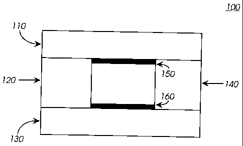
Figure 1 illustrates one embodiment of a Fabry-Perot Phase Shifter. As
illustrated in Figure 1, a Fabry-Perot Phase Shifter (FPPS) 100 is a one-sided
Fabry-Perot
etalon having partially reflective front material 160 and highly reflective
back material
150. As described in greater detail below, the phase and intensity response of
FPPS 100
is wavelength dependent.
In one embodiment, FPPS 100 includes front plate 130, back plate 110, and
spacers 120 and 140. FPPS 100 also includes front reflective material 160 and
back
reflective material 150. In one embodiment, front plate 130 and back plate 110
are glass
(e.g., SiOz) plates and spacers 120 and 140 are made of ultra-low expansion
(ULE)
material. Other materials can be used.
In one embodiment, front reflective material 160 has a reflectivity in the
range of
10% to 25% reflective (e.g., 151%, 19.6%); however, front reflective materials
having
other reflectivities can also be used. Thus, front reflective material 160
reflects 10% to
25% of the optical signal that passes through front glass plate 130. The
remaining 75% to
90% of the signal is passed through front reflective material 160 through the
gap between
front reflective material 160 to back reflective material 150.
In one embodiment, the gap between front glass plate 130 and back glass plate
110 is air filled. Having an air gap in FPPS 100 allows FPPS 100 to operate on
high
power signals without thermal expansion or other thermal effects because the
signals pass
through air rather than the materials of FPPS 100. In one embodiment, back
reflective
material 150 is 90% to 100% reflective (e.g., 99.8%). Thus, back reflective
material 150
reflects substantially all of the optical signals passed by front reflective
material 160. The
light reflected by back reflective material 150 is passed back through front
reflective
material 160 and front plate 130.
-6-
CA 02328647 2000-12-15
Doc. No. 10-408 CA Patent
Figure 2 is the phase and intensity response of reflected light from a FPPS as
illustrated in Figure 1. The FPPS having a response as illustrated in Figure 2
has a front
reflectivity of 19.6% and a back reflectivity of 99.8%. Other front and back
reflectivities
can be used to provide other phase and intensity responses.
As illustrated in Figure 2, the FPPS provides phase modulation with some
attenuation. Because the phase and intensity response of a FPPS is wavelength
dependent, certain frequencies are attenuated more than other frequencies.
However, the
attenuation provided by the FPPS of Figure 1 is not sufficient to provide
channel filtering.
Thus, the FPPS of Figure 1 alone is not sufficient to operate as an
interleaver/
deinterleaver.
Figure 3 illustrates one embodiment of an unequal path Michelson
interferometer.
As illustrated in Figure 4 below, the phase response is linear, which does not
provide
sufficient pass bands and rejection bands to filter optical signals.
Optical fiber 305 receives, from an external source (not shown in Figure 3),
optical signals corresponding to one or more frequencies. Collimator 310
collimates the
optical signals and passes the optical signals to beam sputter cube 320. Other
types of
beam sputters, for example, mirror beam sputters can also be used. Beam
sputter cube
320 splits the beam received via optical fiber 305 and collimator 310 into a
first sub-beam
and a second sub-beam.
The first sub-beam is reflected by beam sputter cube interface 322 to etalon
360.
Etalon 360 includes reflecting surface 362 that reflects the first sub-beam to
collimator
350. In one embodiment, etalon 360 also includes a front reflecting surface
(not shown in
Figure 3). The second sub-beam passes through beam sputter cube interface 322
to back
surface 324. The second sub-beam is reflected by back surface 324 to beam
sputter cube
interface 322, which reflects the second sub-beam to collimator 350.
Constructive and destructive light interference between the first sub-beam and
the
second sub-beam at beam sputter cube interface 322 cause the output signal to
vary
between being at or near full input strength to being greatly attenuated. The
combined
output signal is carried by optical fiber 355.
CA 02328647 2000-12-15
Doc. No. 10-408 CA Patent
Figure 4 is the phase and intensity response of reflected light from an
unequal
path Michelson interferometer as illustrated in Figure 3. Phase lines 410 and
420
represent the phase of the two sub-beams generated by beam sputter 320 of
Figure 3.
Phase line 410 corresponds to the phase of the first sub-beam that passes
through etalon
360. Phase line 420 corresponds to the phase of the second sub-beam that is
reflected by
back surface 324. Transmission line 430 represents the transmission strength
of the
output signal of Figure 3 for a range of frequencies.
The transfer function of the unequal path Michelson interferometer is a
function
of sine 0~ of the phase difference between the two paths (or arms), 0~ _ ~, -
~Z, where
~, and ~, are the phase of the first path and the second path, respectively.
If the lengths
of the first and second paths are, for example, L and 2L , respectively, then
~, = 2kL ,
~Z =4kL,and ~~=2kL-2m~.
Thus, ~~ is periodic and linear (within the 2~ range) in optical frequency and
the spectral transfer function is sinusoidal in optical frequency. In other
words, the
unequal path Michelson interferometer provides periodic transmission and
attenuation
characteristics. However, the unequal path Michelson interferometer does not
provide
enough flat-band transmission bandwidth for transmission channels or enough
bandwidth
for sufficient adjacent channel isolation. Therefore, the unequal path
Michelson
interferometer is insufficient to operate as an interleaver/deinterleaver.
Figure 5 illustrates one embodiment of an interleaver/deinterleaver having a
50/50 beam sputter cube. When operating as an interleaver,
interleaver/deinterleaver 500
receives a set of optical signals, for example, optical channels as defined by
the
International Telecommunications Union (ITU), and separates the optical
signals into two
subsets, for example, even channels and odd channels. When operating as a
deinterleaver, interleaver/deinterleaver 500 receives two sets of signals, for
example, even
channels and odd channels and interleaves the sets of signals into a superset
having both
even and odd channels, for example, a WDM signal carrying ITU channels 15-72.
In one embodiment, the components of interleaver/deinterleaver 500 are held in
optical contact by atomic force rather than epoxy; however, epoxy can also be
used. In
order to maintain optical contact by atomic force, the thickness of each glass
plate should
_g_
CA 02328647 2000-12-15
Doc. No. 10-408 CA Patent
be consistent within a predetermined tolerance. In one embodiment the
thickness
tolerance for each plate is 1.0 Vim; however, other tolerances can also be
used.
Because of the flatness of the components of interleaver/deinterleaver 500, by
abutting the components to each other, contact is maintained by atomic forces.
In one
embodiment, use of atomic force to maintain optical contact allows material
matching to
within 1.0 Vim. As mentioned above, optical contact by atomic force also
provides better
thermal performance compared to use of epoxy to assemble optical components.
As described in greater detail below, separation of even and odd channels is
useful, for example, for interfacing devices designed for one channel spacing
(e.g., 200
GHz) with devices designed for a different channel spacing (e.g., 100 GHz).
Thus,
devices and/or networks can be upgraded without requiring that all devices be
upgraded,
or network bandwidth can be increased. A deinterleaver can be used to combine
sets of
channels (e.g., even channels and odd channels) into a single set of channels.
Beam sputter cube 520 splits the optical signal into a first sub-beam and a
second
sub-beam. In one embodiment, beam sputter cube 520 splits the beam evenly such
that
each etalon receives a 50% strength version of the input signal. In other
words, beam
sputter cube 520 is a 50/50 beam sputter. Other types of beam sputters can
also be used.
Because a precise 50/50 beam sputter is difficult to manufacture, other beam
splitting
ratios can also be used. In one embodiment, the two crystals of beam sputter
520 are
maintained in optical contact by atomic force.
Assuming a 50/50 beam split by beam sputter cube 520, the first sub-beam is
directed to etalon 530 and the second sub-beam is directed to FPPS 540. The
first sub-
beam is reflected by beam sputter cube interface 522 and directed to etalon
530. In one
embodiment, front reflective material 534 reflects 0% to 10°io of the
signal directed to
etalon 530 by beam splitter cube 520. In one embodiment, the gap between front
reflective material 534 and back reflective material 532 is 0.75 mm; however,
other gap
sizes can also be used. Back reflective material 532 is reflects 90% to 100%
of the signal
passed by front reflective material 534. The reflected first sub-beam is
passed by beam
sputter cube interface 522 to collimator 550.
-9-
CA 02328647 2000-12-15
Doc. No. 10-408 CA Patent
In one embodiment, etalon 530 is coupled to beam sputter cube 520 by optical
contact. In such an embodiment, the gap between etalon 530 and beam sputter
cube 520
can be less than 1.0 pm. In an alternate embodiment, etalon :~30 is coupled to
beam
sputter cube 520 with epoxy; however, the gap between etalon 530 and beam
sputter cube
520 is generally larger than when coupled by atomic force. In one embodiment,
etalon
530 includes tuning plate 560. Tuning plate 560 provides
interleaver/deinterleaver 500
with fine resolution (e.g., 10 nm or less). Tuning plate 560 provides fine
tuning
capability by changing the effective optical path length through etalon 530.
The second sub-beam is passed beam sputter cube interface 522 to FPPS 540. In
one embodiment, front reflective material 542 reflects 15% to 20% of the
second sub-
beam directed to FPPS 540 by beam sputter cube 520. In one embodiment the gap
between front reflective material 542 and back reflective material 544 is I .5
mm;
however, other gap sizes can also be used. Back reflective material 544
reflects 90% to
100% of the signal passed by front reflective material 542. The reflected
second sub-
beam is directed to beam sputter cube interface 522 and reflected to
collimator 550. In
one embodiment, FPPS 540 is coupled to beam sputter cube 520 by atomic force.
In an
alternate embodiment, FPPS 540 is coupled to beam sputter cube 520 with epoxy.
Etalon 530 provides a linear phase difference and a sinusoidal transfer
function, as
described above with respect to Figures 3 and 4, for the first sub-beam. FPPS
540
provides a non-linear phase response with slight attenuation, as described
above with
respect to Figures 1 and 2, for the second sub-beam. The phase and intensity
response of
etalon 530 and FPPS 540 cause constructive and destructive light interference
at beam
sputter cube interface 522. The frequencies for which constructive light
interference
occurs are passed at or near full intensity. The frequencies for which
destructive light
interference occurs results in attenuation of the optical signal..
When operating as a deinterleaver, as described above with respect to Figure
5,
interleaver/deinterleaver 500 receives a set of signals via optical fiber 505
and separates
the optical signals into two subsets. Interleaver/deinterleaver 500 operates
to pass a first
subset of signals to optical fiber 555 and to reflect a second subset of
optical signals back
to optical fiber 505 to separate the optical signal into two subsets of
optical signals. An
CA 02328647 2000-12-15
Doc. No. 10-408 CA Patent
optical circulator can be coupled to optical fiber 505 to carry the input and
output signals
to and from collimator 510.
When operating as an interleaver, interleaver/deinterleaver S00 receives a
first set
of optical channels (e.g., even channels) via optical fiber 555 and a second
set of optical
channels (e.g., odd channels) via optical fiber 505. Interleaver/deinterleaver
500 operates
to pass the first set of optical channels from optical fiber 555 to optical
fiber 505 and
reflect the second set of optical channels from optical fiber 505 back to
optical fiber 505
to combine the two sets of optical signals into a superset of optical signals.
An optical
circulator (not shown in Figure 5) can be coupled to optical fiber 505 to
carry the input
and output signals to and from collimator 510.
Because even and odd channels have a frequency spacing that is double the
frequency spacing for the combined set of channels, interleavers and
deinterleavers can be
used to interface devices designed for different channel spacings. For
example, in a 100
GHz spaced scheme, the odd channels are spaced by 200 GHz and the even
channels are
spaced by 200 GHz. By separating the even and odd channels, devices that are
designed
to operate with 200 GHz spaced channels can interface with 100 GHz spaced
devices.
Other frequency ratios (e.g., 100 GHz, 50 GHz) can be similarly interfaced.
In one embodiment, interleaver/deinterleaver 500 is assembled according to the
following procedure. Incoming parts are inspected to determine whether the
parts satisfy
a set of predetermined specifications. For example, typical glass thickness
variation is
approximately ~1.0 pm; however, as manufacturing procedures improve, the
tolerances
can be correspondingly reduced.
Beam sputter cube 520, etalon 530 and/or FPPS 540 are assembled by abutting
the sub-components together such that the sub-components are held together by
atomic
force. Beam splitter cube 520, etalon 530 and FPPS 540 are coupled by abutment
such
that they are maintained in contact by atomic force.
Because the components of interleaver/deinterleaver 500 are coupled by atomic
force with no epoxy between the optical elements, interleaver/deinterleaver
500 can be
designed and built with sub-micron tolerances, which is necessary for sub-100
GHz FSR.
CA 02328647 2000-12-15
Doc. No. 10-408 CA Patent
Coupling of optical sub-components and elements with atomic force improves
thermal
performance of interleaver/deinterleaver 500.
A tuning plate holder fixture (not shown in Figure 5) is coupled to beam
splitter
cube 520, etalon 530 and/or FPPS 540 to form the interleaver core. The tuning
plate
holder fixture can be coupled with epoxy. Tuning plate 560 is disposed within
etalon 530
and connected to the tuning plate holder fixture.
The interleaver core with tuning plate 560 is attached to a package (e.g., a
metallic
case) in any manner known in the art. Temperature cycling can be performed if
desired.
The angle of tuning plate 560 is adjusted to tune interleaver/deinterleaver
500. In one
embodiment, the output power and optical spectrum are monitored to tune
interleaver/de-
interleaver 500. Collimators 510 and 550 are soldered in place and tuning
plate 560 is
maintained in place by epoxy. The package is sealed and
interleaver/deinterleaver 500
assembly is complete.
Figure 6 is the phase and intensity response of an interleaver/deinterleaver
as
illustrated in Figure 5. By combining an FPPS and a Michelson interferometer,
a periodic
non-linear phase response can be achieved. As a result, periodic flat-band
bandwidth can
be provided. Also provided is enough bandwidth with large isolation necessary
to isolate
optical channels and operate as an optical interleaver/deinterleaver.
Phase line 610 corresponds to the phase of the first sub-beam that is directed
to
etalon 530 as a function of frequency. Phase line 620 corresponds to the phase
of the
second sub-beam that is directed to FPPS 540 as a function of frequency.
Transmission
line 630 indicates transmission intensity of optical signals output by the
interleaver as a
function of frequency.
When phase lines 610 and 620 are in phase or 180° out of phase, the
interleaver/
deinterleaver transmits the optical signals at or near full intensity. As
phase lines 610 and
620 become out of phase with respect to each other the intensity of the
optical signals
decreases and the signal is attenuated. Because phase line is periodic and non-
linear,
transmission line 630 indicates regularly spaced frequencies corresponding to
relatively
wide, flat pass bands.
-~2-
CA 02328647 2004-06-15
Doc, No. 10-408 CA Patent
Transmission of the optical signals at or near full intensity occurs when the
two
sub-beams are in phase or are 180° out of phase because of constructive
light interference
at beam sputter cube interface 522. When the two sub-beams are out of phase,
destructive interference at beam splitter cube interface 522 causes the two
sub-beams to
cancel each other, which results in attenuation of the original optical
signal.
Figure 7 illustrates certain dimensions for one embodiment of a Michelson
phase
shifter interleaver/deinterleaver. The dimensions described are used to tune
the
interleaver/deinterleaver to separate even and odd ITU channels from a WDM
input
signal and to combine even and odd ITU channels to output a WDM signal. Other
dimensions can be used for other filtering characteristics.
2L is the length of the air gap of FPPS 540;
L, is the distance between the midpoint of the beam splitter cube interface
and the
surface to which FPPS 540 is coupled;
LZ is the distance between the midpoint of the beam splitter cube interface
and the
surface to which etalon 530 is coupled;
L3 is the thickness of the front plate of FPPS 540;
L4 is the thickness of the front plate of etalon 530;
LS is the length of the air gap of etalon 530; and
L6 is the thickness of the tuning plate.
In one embodiment, the length air gap of FPPS 540, 2L , is determined
according
to:
2L=cl2/FSR
where c is the speed of light and FSR is the free spectral range, or the
frequency
difference between channels to be filtered. For 50 GHz channel spacing 2L =
2.9971 mm
and for 100 GHz channel spacing 2L =1.4986 mm.
In one embodiment the following phase matching conditions are used:
L = LS + Lb.f ~~)+ ~~L4 - L3 ~+ ~~LZ - Lu
where
-13~
CA 02328647 2004-06-15
Doc. No. 10-408 CA Patent
f.(~) - n - cos(~ - ø ) , f.(0) _ (n - l~, ~' = sin-1 sin ~ , and n is the
index of
~os cos
refraction for the material through which the optical signal passes, and the
following
design parameters are used:
Ll ~ Lz ~ l0;um for a beam splitter embodiment,
L6 = L4 =1.5 mm, which are chosen values,
L3 = L4 + L~ =3 mm,
L6 - LS ~ L =1.4985 mm fox 100 GHz spacing, and
L6 - LS ~ L =0.74925 mm for 50 GHz spacing.
Figure 8a illustrates one embodiment of a Michelson phase shifter interleaver/
deinterleaver having two inputloutput ports arranged with near normal
incidence with
respect to the beam splitter cube. In one embodiment, both collimators (510
and 550) are
arranged with near normal incidence (i.e., nearly perpendicular) with respect
to the
surface beam splitter cube 520.
When operating as a deinterleaver, a WDM or DWDM optical signal having odd
and even ITU channels is carried by optical fiber 810 to circulator 800.
Circulator 800
directs the optical signal to optical fiber 505, which carries the optical
signal to collimator
510. Interleaver/deinterleaver 500 operates as described above to separate the
set of
optical signals into subsets of even and odd channels.
One subset of optical channels (e.g., even channels) is output via collimator
550 to
optical fiber 555. The second subset of optical channels (e.g., odd channels)
is output via
collimator 510 to optical fiber 505. The second subset of optical channels is
carried by
optical fiber 505 to circulator 800, which directs the second subset of
optical channels to
optical fiber 820.
When operating as an interleaver, interleaver/deinterleaver 500 receives a set
of
optical channels (e.g., even channels) from optical fiber 555 via collimator
550. A
second set of optical channels (e.g., odd channels) is carried by optical
fiber 820 and
directed to optical fiber 505 by circulator 800. Interleaver/deinterleaver 500
receives the
second set of optical signals from fiber 505 via collimator 510.
Interleaver/deinterleaver
-14-
CA 02328647 2000-12-15
Doc. No. 10-408 CA Patent
500 combines the sets of optical signals into a superset of optical signals
having both
even and odd channels as described above.
The superset of optical signals is output to collimator 505 via 510.
Circulator 800
directs the superset of optical signals to optical fiber 810. Thus, when
collimators 510
and 550 are arranged with normal incidence with respect to beam sputter cube
520, a
circulator (e.g., circulator 800) is used to direct input and output signals
through
collimator 510.
Figure 8b illustrates one embodiment of a Michelson phase shifter interleaver/
deinterleaver having two input/output ports arranged with angled incidence
with respect
to the beam sputter cube. In one embodiment, collimators 830 and 840 are
arranged with
an angled incidence with respect to the surface of beam sputter cube 520 while
collimator
850 is arranged with normal incidence with respect to the surface of beam
sputter cube
520. In one embodiment, collimators 830 and 840 are arranged with
3~0.12° incidence
(i.e., approximately 3° away from perpendicular) and 6~024°
angle between collimators
830 and 840 (i.e., approximately 6° away from parallel).
Collimator 550 and optical fiber 555 are arranged and operate in the same
manner
as with Figure 8a. When operating as a deinterleaver, the input optical signal
is received
from optical fiber 835 via collimator 830. The channels of the optical signal
are
separated as described above; however, because of the angle of incidence of
the input
signal, the output signal to optical fiber 845 though collimator 840 has the
same angle of
incidence. Because the input and output optical signals are separated, a
circulator is not
necessary. In one embodiment, collimators 830 and 840 are replaced by a dual-
fiber
collimator to receive optical fibers 835 and 845.
When operating as an interleaver, even and odd channels are received by
collimators 840 and 550 from optical fibers 845 and 555, respectively. The
even and odd
channels are combined as described above and output to optical fiber 835 via
collimator
830.
Figure 8c illustrates one embodiment of a Michelson phase shifter interleaver/
deinterleaver having a two-fiber input/output port and a single-fiber
input/output port,
both of which are arranged with near normal incidence with respect to the beam
sputter
-15-
CA 02328647 2000-12-15
Doc. No. 10-408 CA Patent
cube. In one embodiment, dual-fiber collimator 850 and single-fiber collimator
550 are
arranged with an normal incidence with respect to the surface of beam splitter
cube 520.
Dual-fiber collimator 850 includes a walk-off element such as, for example, a
walk-off
crystal to direct optical signals to and from the appropriate fiber.
Collimator 550 and optical fiber 555 are arranged and operate in the same
manner
as with Figures 8a and 8b. When operating as a deinterleaver, the input
optical signal is
received from optical fiber 857 via collimator 850. The channels of the
optical signal are
separated as described above and the output signals are directed to optical
fiber 855 via
collimator 850 and to optical fiber 555 through collimator 550. Because the
input and
output optical signals are separated, a circulator is not necessary.
When operating as an interleaver, even and odd channels are received by
collimators 850 and 550 from optical fibers 855 and 555, respectively. The
even and odd
channels are combined as described above and output to optical fiber 857 via
collimator
850.
Figure 9a is a transmission plot for a Michelson phase shifter interleaver/de-
interleaver operating as a deinterleaver with an input/output port having near
normal
incidence and where the FPPS has a reflectivity of 12%. Transmission line 900
corresponds to a first port to pass a first subset of optical signals (e.g.,
even channels) and
transmission line 910 corresponds to a second port to pass a second subset of
optical
signals (e.g., odd channels).
Figure 9b is a transmission plot for a Michelson phase shifter interleaver/de-
interleaver operating as a deinterleaver with an input/output port having near
normal
incidence and where the FPPS has a reflectivity of 16%. Transmission line 920
corresponds to a first port to pass a first subset of optical signals (e.g.,
even channels) and
transmission line 930 corresponds to a second port to pass a second subset of
optical
signals (e.g., odd channels).
Figure 9c is a transmission plot for a Michelson phase shifter interleaver/de-
interleaver operating as a deinterleaver with input and output ports having 3
° incidence
and where the FPPS has a reflectivity of 16%. Transmission line 940
corresponds to a
first port to pass a first subset of optical signals (e.g., even channels) and
transmission
-16-
CA 02328647 2000-12-15
Doc. No. 10-408 CA Patent
line 950 corresponds to a second port to pass a second subset of optical
signals (e.g., odd
channels).
Figure 9d is a transmission plot for a Michelson phase shifter interleaver/de-
interleaver operating as a deinterleaver with input and output ports having
3° incidence
and where the FPPS has a reflectivity of 20%. Transmission line 960
corresponds to a
first port to pass a first subset of optical signals (e.g., even channels) and
transmission
line 970 corresponds to a second port to pass a second subset of optical
signals (e.g., odd
channels).
Figure 10 illustrates certain dimensions for one embodiment of a Michelson
phase shifter interleaver/deinterleaver with a contact plate sputter. In one
embodiment,
the air gap dimensions, the phase matching parameters and the design
parameters are the
same for the interleaver with the contact plate as with the interleaver with
the beam
sputter with the following exception:
L, ~ L, ~ O.S,um for a plate sputter embodiment.
The arrows of Figure 10 indicate signal paths when interleaver/deinterleaver
1090
operates as a deinterleaver. Input and output paths are reversed when
interleaver/deinter-
leaver 1090 operates as an interleaver. In general, interleaver/deinterleaver
1090 operates
in a similar manner as the beam sputter cube interleaver/deinterleavers
described above.
In one embodiment, plate sputter 1000 is a 50/50 beam sputter; however, other
plate
splitters can be used. In one embodiment crystals 1002 and 1004 are silica;
however,
other materials can also be used.
In one embodiment, FPPS 1010 and etalon 1020 are coupled to contact plate
splitter 1006 by atomic force. Coupling with atomic force allows the gaps
between FPPS
1 O10 and contact plate sputter 1006 and between etalon 1020 and contact plate
sputter
1006 to be less than 1.0 Vim. In an alternate embodiment, FPPS 1010 and etalon
1020 are
coupled to contact plate sputter 1006 by epoxy. As mentioned above, coupling
with
atomic force improves both thermal and optical performance.
When operating as a deinterleaver, an interleaved optical signal is received
from
optical signal 1030 through collimator 1035. In one embodiment the optical
signal has a
3~0.12° incidence angle; however, other angles can also be used. The
incident angle can
_17_
CA 02328647 2004-06-15
Doc, No. 10-408 CA Patent
be varied (e.g., by ~0.12°) to fine tune the filtering characteristics
of interleaver/deinter-
leaver 1090. In one embodiment, ~0.12° incident angle adjustment
corresponds to a ~20
GHz FSR adjustment.
The optical signal passes through crystal 1002 to plate sputter 1000. In one
embodiment, plate sputter passes 50% of the intensity of the optical signal
and reflects
the other 50% of the intensity of the optical signal. Thus, plate sputter 1000
is a 50/50
plate sputter; however, other plate sputters can also be used.
The reflected optical signal passes through crystal 1002 to FPPS 1010. A phase
shifted version of the optical signal is reflected back to plate sputter 1000.
The optical
passes through crystal 1004 to etalon 1020. A version of the optical signal
having a linear
phase difference is reflected back to plate splitter 1000.
At plate sputter 1000, the reflected signals converge and, through
constructive and
destructive interference, are separated into even and odd channels. One set of
channels
(e.g., even channels) is directed to optical fiber 1050 via collimator 1055.
The second set
of signals (e.g., odd channels) is directed to optical fiber 1040 via
collimator 1040.
In one embodiment, tuning plate 1060 is used to fine tune the phase
characteristics
of interleaver/deinterleaver 1090. Tuning plate 1060 operates in a similar
manner as
tuning plate 560 described above. In one embodiment, a ~0.01 °
adjustment to tuning
plate 1060 corresponds to a ~10 nm phase distance.
The collimators (1035, 1045 and 1055) are oriented at a predetermined angle
away from normal with respect to the surfaces of the crystals of
interleaver/deinterleaver
1090. In one embodiment, the angle is 3 ~0.12°; however, other angles
can be used, for
example, with different crystal dimensions.
When operating as an interleaves, even and odd channels are received by
collimators 1045 and 1055 from optical fibers 1040 and 1050, respectively. The
even and
odd channels are combined as described above and output to optical fiber 1030
via
collimator 1035.
In one embodiment, interleaver/deinterleaver 1090 is assembled according to
the
following procedure; however, similar interleaver/deinterleaver devices can be
assembled
according to slightly different procedures. Incoming parts are inspected to
determine
-18-
CA 02328647 2000-12-15
Doc. No. 10-408 CA Patent
whether the parts satisfy a set of predetermined specifications. For example,
current
crystal thickness variation is approximately ~1.0 Vim; however, as tolerances
improve, the
specifications can be correspondingly reduced.
Contact plate sputter 1006, etalon 1020 and/or FPPS 1010 are assembled by
abutting the sub-components together such that the sub-components are held
together by
atomic force. Contact plate sputter 1006, etalon 1020 and/or FPPS 1010 are
coupled by
abutment such that they are maintained in contact by atomic force.
Because the components of interleaver/deinterleaver 1090 are coupled by atomic
force with no epoxy between the optical elements, interleaver/deinterleaver
1090 can be
designed and built with sub-micron tolerances, which is necessary for sub-100
GHz FSR.
Coupling of optical sub-components and elements with atomic force improves
thermal
performance of interleaver/deinterleaver 1090.
A tuning plate holder fixture (not shown in Figure 10) is coupled to contact
plate
sputter 1006, etalon 1020 and FPPS 1010 to form the interleaver core. The
tuning plate
holder fixture can be coupled with epoxy or by atomic force. Tuning plate 1060
is
disposed within etalon 1020 and connected to the tuning plate holder fixture.
The interleaver core with tuning plate 1060 is attached to a package (e.g., a
metallic case) in any manner known in the art. Temperature cycling can be
performed if
desired. The incidence angle for collimators 1035, 1045 and 1055 and the angle
of tuning
plate 1060 are adjusted to tune interleaver/deinterleaver 1090. In one
embodiment, the
output power and optical spectrum are monitored to tune
interleaver/deinterleaver 1090.
Collimators 1035, 1045 and 1055 are soldered in place and tuning plate 1060 is
maintained in place by epoxy. The package is sealed and
interleaver/deinterleaver 1090
assembly is complete.
Figure lla is a plot of change in optical path length versus tuning plate
angle, ~,
for one embodiment of an interleaver/deinterleaver having a tuning plate. The
plot of
Figure 11 a illustrates course tuning of an interleaver/deinterleaver having
an etalon with a
tuning plate. The plot of Figure 11 a is for a tuning plate having a thickness
of 1500 Vim.
In one embodiment, the function of change in optical path length is:
L~(f ~~) - .f ~0)~
-19-
CA 02328647 2000-12-15
Doc. No. 10-408 CA Patent
where f (~~ and f ~0~ are the functions described above. Thus, as the tuning
plate is
rotated, the optical path length changes in a non-linear fashion.
For example, when the tuning plate is rotated to an angle of 5° away
from parallel
with the front and back plates of the etalon, the optical path length of the
etalon is
increased by approximately 1500 Vim. As another example, if the tuning plate
is rotated
to an angle of 8° away from parallel with the front and back plates of
the etalon, the
optical path length is increased by 4600 pm.
Figure llb is a plot of differential change in optical path length by when
4~=0.01 ° versus tuning plate angle, ~, for one embodiment of an
interleaver/deinterleaver
having a tuning plate. The plot of Figure 1 lb illustrates fine tuning of an
interleaver/deinterleaver having an etalon with a tuning plate. The plot of
Figure l lb is
for a tuning plate having a thickness of 1500 Vim.
The plot of Figure 11 b illustrates the change in optical path length for each
0.01 °
change in the position of the tuning plate for starting angles in the range of
0° to 10°. For
example, if the tuning plate is at an angle of 5° away from parallel
with respect to the
front and back plates of the etalon, an increase of the tuning plate angle by
0.01 ° results in
a 7 nm increase in the optical path. In other words, at an angle of 5°,
the tuning plate
provides 7 nm resolution. As another example, if the tuning plate is at an
angle of 2°
with respect to the front and back plates of the etalon, an increase of the
tuning plate
angle of 0.01 ° results in a 5 nm increase in the optical path length,
or a resolution of 5 nm
at 2°.
Figure 12 is a conceptual illustration of a conversion from an optical channel
scheme having 100 GHz spacing to an optical channel scheme having 200 GHz. The
conversion of Figure 12 is useful, for example, to allow devices designed to
operate with
an optical channel scheme having 200 GHz channel spacing to interact with
other devices
or a network designed to operate with an optical channel scheme having 100 GHz
channel spacing. Conversion between 100 GHz channel spacing and 200 GHz
channel
spacing allows, for example, network bandwidth to be increased without
upgrading all of
the devices that interact with the network.
-20-
CA 02328647 2000-12-15
Doc. No. 10-408 CA Patent
In one embodiment, the converter of Figure 12 is a deinterleaver that
separates an
optical signal having even and odd channels (e.g., ITU channels) into a first
optical signal
including the even channels and a second optical signal including the odd
signals. After
the signals are deinterleaved, the odd channels have a 200 GHz spacing and the
even
channels have a 200 GHz spacing. Recombining the even and the odd channels can
be
accomplished with an interleaver that combines the odd channels and the even
channels
into a single optical signal. In other words, the even and odd channels having
200 GHz
spacing are combined (interleaved) into an optical signal having 100 GHz
signal spacing.
Similar interleaving can be provided to convert between 50 CiHz spaced
channels and 100
GHz spaced channels, as well as between other sets of channel spacing schemes.
Figure 13 is a block diagram of an optical deinterleaver for conversion from
an
optical channel scheme having 50 GHz spacing to an optical channel scheme
having 1300
GHz spacing. In general, deinterleaver 1300 includes deinterleaver 1310 to
convert from
one set of 50 GHz spaced channels to two sets of 100 GHz spaced channels.
Deinterleaver 1300 also includes two deinterleavers (1320 and 1330) each of
which
convert one of the sets of 100 GHz spaced channels to two sets of 200 GHz
spaced
channels. Deinterleaver 1300 allows devices designed for 200 GHz spaced
channels to
interact with devices or networks designed for 50 GHz spaced channels.
Optical fiber 1305 carries a set of optical channels, i , having 50 GHz
spacing.
Deinterleaver 1310 separates the set of optical channels into sets of even,
2(j + 1), and
odd, 2 j + 1, channels. The even channels are input to deinterleaver 1330 and
the odd
channels are input deinterleaver 1320. The even and the odd channels have 100
GHz
spacing.
Deinterleavers 1320 and 1330 operate to further separate the set of optical
channels. Conceptually, deinterleaver 1320 and 1330 operate on the respective
100 GHz
spaced channels to separate the input channels into "even" and "odd" channels.
The sets
of channels output by deinterleavers 1320 and 1330 have 200 GHz spacing.
Deinterleaver 1320 separates the odd channels into two sets of channels, odd-
odd
channels, 4k + 1, output by optical fiber 1340 and odd-even, 4k + 2 , channels
output by
optical fiber 1350. Deinterleaver 1330 separates the even channels into two
sets of
-21-
CA 02328647 2000-12-15
Doc. No. 10-408 CA Patent
channels, the even-odd, 4k + 3 , channels output by optical fiber 1360 and the
even-even,
4~k + l~, channels output by optical fiber 1370.
The four sets of channels output by deinterleaver 1300 are 200 GHz spaced
channels. Thus, deinterleaver 1300 can be used to interface one or more
devices designed
to operate on 200 GHz spaced channels with one or more devices or networks
designed to
operate on 50 GHz spaced channels. Other channel spacings can also be
supported.
Figure 14 is a block diagram of an optical interleaves for conversion from an
optical channel scheme having 200 GHz spacing to an optical channel scheme
having 50
GHz spacing. In general, interleaves 1400 includes interleaves 1410 to convert
from two
sets of 200 GHz spaced channels to one set of 100 GHz spaced channels.
Similarly,
interleaves 1420 converts from two sets of 200 GHz spaced channels to one set
of 100
GHz channels. Interleaves 1430 converts the two sets of 100 GHz spaced
channels to one
set of 50 GHz spaced channels. Interleaves 1400 allows devices designed for
200 GHz
spaced channels to interact with devices or networks designed for 50 GHz
spaced
channels.
The odd-odd, 4k + 1, channels having 200 GHz spacing are input to interleaves
1410 via optical fiber 1440. The odd-even, 4k + 2 , channels having 200 GHz
spacing are
input to interleaves 1410 via optical fiber 1450. Interleaves 1410 interleaves
the odd-odd
channels and the odd-even channels to generate a set of odd, 2 j + 1, channels
having 100
GHz spacing.
The even-odd, 4k + 3 , channels having 200 GHz spacing are input to
interleaves
1420 via optical fiber 1460. The even-even, 4~k + 1~ , channels having 200 GHz
spacing
are input to interleaves 1420 via optical fiber 1470. Interleaves 1420
interleaves the even-
odd channels and the even-even channels to generate a set of even, 2~ j + 1~,
channels
having 100 GHz spacing.
Interleaves 1430 interleaves the even and odd channels to generate a set of
channels, i , having 50 GHz spacing. Thus, interleaves 1400 allows devices
designed to
operate on optical channels having 200 GHz spacing to interact with devices
designed to
operate on optical channels having 50 GHz spacing. Other channels spacings can
also be
supported.
-22-
CA 02328647 2000-12-15
Patent
Doc. No. 10-408 CA
In the foregoing specification, the invention has been described with
reference to
specific embodiments thereof. It will, however, be evident that various
modifications and
changes can be made thereto without departing from the broader spirit and
scope of the
invention. The specification and drawings are, accordingly, to be regarded in
an
illustrative rather than a restrictive sense.
-23-