Note : Les descriptions sont présentées dans la langue officielle dans laquelle elles ont été soumises.
.r
CA 02329209 2001-02-27
MAGNETIC FIELD SENSING DEVICE
BACKGROUNn OF THE INVENTION
1. FIELD OF THE INVENTION:
S The present invention relates generally to magnetic field sensing devices
and
specifically to magnetic field sensing devices capable of sensing magnetic
fields along
two mutually perpendicular axis. Such two axis magnetic field sensors are
required in
many applications. Electronic compasses, magnetic field probes and virtual
reality are a
few examples ofapplications where two axis magnetic field sensors are useful.
2. DESCRIPTION OF THE PRIOR ART
In the past, two axis magnetic field sensors were typically constructed using
two
single axis magnetic sensors. For example, U.S. Patent 5,247,278 describes a
single
axis magnetic field sensor including an integral current strap for setting a
direction of
magnetization. Two of the sensing devices described in U.S. Patent 5,247,278
can be
used to form a two-axis magnetic field sensing device. For simplicity, two-
axis
magnetic field sensing devices will be referred to herein as an x-axis sensor
and a y-axis
sensor, meaning that the two axis are perpendicular. In the past, the two
single axis
sensors could be housed in a single package enclosure and oriented so that
their
2 0 sensitive directions were perpendicuiar to each other. Alternatively two
single-axis
individually-packaged die could be mounted on a circuit board with the
sensitive axis of
each die perpendicular to the other dic. There are disadvantages to the use of
two single
axis die. One disadvantage of this approach is that it requires extra assembly
effort
either at the package level or at the board level. In addition it is difficult
to locate the
2 5 two single-axis die so that they are orthogonal to each other. The bcst
control on the
orthogonality of the two single-axis parts in high volume manufacture may be
on the
order of t 1 °, which induces the same level error on compass heading.
A magnetoresistive sensor capable of measuring a low magnetic field requires
that the magnetic moment be initially aligned in one direction, which usually
is
3 0 perpendicular to the sensitive direction of the sensor. With a uniform
external magnetic
field to initialize the alignment of magnetic moment, it is almost impossible
to have an
x-axis and a y-axis sensors on a single chip. In addition, generally a
magnetic film used
for magnetoresistive~sensors will have its own crystal easy axis which is
determined by
CA 02329209 2001-02-27 _
-2-
a magnetic field applied during the deposition of the magnetic film. Single
axis sensors
typically utilize this easy axis and initially align the magnetic moment along
it. Single
axis magnetoresistive sensors usually have the crystal anisotropic field and
the shape
anisotropic field in the same direction to guard against magnetic and thermal
disturbances and to maintain a stable and low noise sensor output. The
stability of a
magnetoresistive sensor is determined at least to some extent by how good it
maintains
a single magnetic domain state after the magnetic field for aligning or
setting the
magnetization is removed.
An integrated two-axis magnetoresistive sensor must have a sensitive direction
in an x-axis and a sensitive direction along a y-axis. This means that at
least one of the
sensor's directions can not be aligned with the crystal easy axis direction.
Therefore
consideration must be given to how to deal with the crystal easy axis when
attempting to
construct a two-axis sensor on a single die, and how to initially align the
magnetic
moment in both an x direction and a y direction.
The advantage of a two-axis sensor on one die is that the orthogonality of the
two
sensors is controlled by the photolithography method, which has accuracy in
the range
of about 0.01 °.
Thus a need exists for an integrated two-axis magnetoresistive sensor.
2 o SUMMARY OF THE INVENTI(,~V
The present invention solves these and other needs by providing a two-axis
integrated device for measuring magnetic fields including two sensor units
formed from
magnetoresistive material having a crystal anisotropy field direction.
Elements of the
first sensor unit have a total anisotropy field in a first dircction. Elements
of the second
2 5 sensor unit have a total anisotropy field in a second direction which is
perpendicular to
the first direction. Means are provided for setting a direction of
magnetization in the
elements of the first and second sensor units. An output of the first sensor
unit is
representative of magnetic field components perpendicular to the first
direction and an
c
output of the second sensor is representative of magnetic field components
3 0 perpendicular to the second direction.
CA 02329209 2001-02-27
-3-
BRIEF DESCRIPTION OF TFIE DRAWINGS
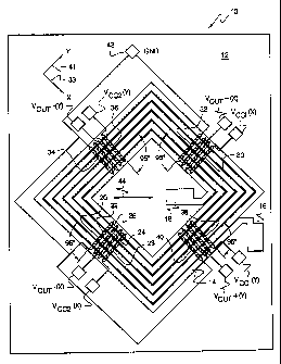
FIG. 1 shows a top plan view of a simplified integrated circuit layout
according
to the teachings of the present invention.
FIG. 2 shows a diagrammatic representation of certain principles according to
the teachings of the present invention.
FIG. 3 shows certain additional details of the circuit layout of FIG. 1.
DETAILED DESCRIPTION
A device for sensing magnetic field components along two axis is shown in the
drawings and generally designated 10. Fig. 1 shows an integrated circuit
layout for a
magnetic field sensor in accordance with the present invention. An integrated
circuit die
12 has formed thereon a conductor or strap 14 which extends from set or set
reset pad 16
in a clockwise four sided spiral form and terminates in pad I 8.
Magnetoresistive
elements are formed of elongated strips of magnetoresistive material. Fig. 1
shows for
example an element 20 consisting of magnetoresistive strips 22 and 24 and
interconnect
26. Only two magnetoresistive strips per element are shown for simplicity, but
it is
understood that an actual element could include many more strips. Elements 20,
28, 30,
and 32 are shown connected in a first Wheatstone bridge arrangement with a
power
supply connection at Vcc 1 (X) and Vcc2(?~) and an output voltage connection
between
2 0 Vout+(X) and Vout-{X). The direction of sensitivity of the first
Wheatstone bridge is
shown by arrow 33 and this bridge acts as the x-axis sensor.
Elements 34, 36, 38 and 40 are shown connected as a second Wheatstone Bridge
arrangement with a power supply connection at Vccl(Y) and Vcc2(Y) and an
output
voltage connection bctween Vout+(Y) and Vout-(Y). In Fig. l, separate power
supply
2 5 connections are shown, however they are connected to one common power
supply. The
direction'of sensitivity of the second Wheatstone bridge is shown by arrow 41
and this
bridge acts as the Y axis sensor. Conductive paths as shown in FIG. 1 connect
one end
of each of elements 20 and 32 of the first Wheatstone bridge and one end of
elements 34
and 40 of the second Wheatstone bridge to ground pad 42. Now that the basic
3 0 construction of magnetic field sensing device 10 has been disclosed, the
operation of
device 10 according to the teachings of the present invention can be set forth
and
appreciated.
In the two-axis device of the present invention, the X sensor and the Y sensor
must have sensitive directions perpendicular to each other. In the specific
embodiment ,
CA 02329209 2001-02-27
-4-
of Fig. 1 the easy axis 44 of the crystal anisotropy field of the
magnetoresistive material
film is in one direction, that is, it is either 0° or 180° for
both the x-axis portion and the
y-axis portion of the two sensor units formed in the material. The direction
is
determined by magnetic field direction during the deposition and annealing of
the
S magnetoresistive material. Other embodiments of the present invention could
use films
that do not have a crystal anisotropy field.
The construction and operation of the two-axis magnetic field sensing device
of
the present invention will be explained by reference to the use of elongated
strips of a
magnetoresistive material such as Permalloy which are interconnected. Various
other
constructions are possible.
An elongated strip of magnetoresistive material may be considered to have an
associated crystal anisotropy field and a shape anisotropy field. The total
anisotropy
field is the vector sum of the crystal anisotropy field and the shape
anisotropy field.
Fig. 2 shows, according to the principles of the present invention, the
relationship of the
anisotropy fields. Fig. 2 shows, for the x-sensor, the easy axis 46 of the
crystal
anisotropy field, the easy axis 48 of the shape anisotropy field, and the easy
axis 50 of
the total anisotropy field. The easy axis 48 of the shape anisotropy field is
along the
length of the elongated strip. By way of example and not by way of a
limitation, the
crystal anisotropy field may be about 3 Oersted (Oe), and the shape anisotropy
field
2 0 about 25 Oe. In this example, the shape anisotropy field 48 is displaced
from the crystal
anisotropy field 46 by about 50° in order to cause the total anisotropy
field SO to be
displaced from the crystal anisotropy field 46 by about 45°. Fig. 2
also shows for the y-
sensor, the easy axis 52 of the crystal anisotropy field, the easy axis 54 of
the shape
anisotropy field, and the easy axis 56 of the total anisotropy field. The easy
axis 54 of
the shape anisotropy field is along the length of the elongated strip.
Thus for each of the sensors, the total anisotropy field is the vector sum of
the crystal
anisotropy field and the shape anisotropy field. The sensitive direction of a
sensor will
be in a direction perpendicular to the total anisotropy field. In order to
arrange two
sensors on a single die or chip to be sensitive in two mutually perpendicular
directions,
3 0 the total anisotropy field of the two sensors must be perpendicular to
each other. In the
preferred embodiment of Fig. I, device ~0 is constructed with the x-axis
sensor and the
y-axis sensor arranged symmetrically relative to the crystal easy axis 44 of
the
magnetoresistive material. For the specific embodiment of FIG. 1, the elements
of the
CA 02329209 2001-02-27
-5-
x-axis sensor, i.e., elements 20, 28, 30 and 32, are rotated counterclockwise
from the
crystal axis by about 50° and the elements of the y-axis sensor, i.e.,
elements 34, 36, 38
and 40, are rotated clockwise by about 50°.
FIG. 3 shows a magnetoresistive strip 60 of the type that could be used to
make
up the bridge elements shown in FIG. 1. A conductive strip 62 extends across
strip 60
and makes an angle 64 of about 50° with strip 60. This angle, of
course, will depend on
the relationship of the crystal anisotropy field, shape anisotropy field and
total
anisotropy field for the spccific device.
In the traditional design of elements using elongated magnetoresistive strips
the
barberpoles have been located at plus or minus 45° to the strips.
According to the
teachings of the present invention, the width of the barberpoles, the gap
between
barberpoles, and orientation relative to the magnetoresistive strip need to be
optimized
to provide an average current flow in the magnetoresistive material that is
within about
~45° to the easy axis of total anisotropy fields in both X and Y
sensors. In the present
invention, within the borders of minimum width and maximum gap, the current
flow
direction mainly is determined by the barberpole orientations. The barberpole
orientations for a specific element are either along the crystal anisotropy
field direction
or perpendicular to the crystal anisotropy field direction, depending on the
position of
the element in the Wheatstone bridge.
2 0 Now that the construction and operation of device 10 have been described,
additional advantages can be set forth and appreciated. A single coil 14 may
be used as
a set coil or set/reset coil for both the X sensor and the Y sensor. Coil 14
provides
alignment along the total anisotropic field direction for both the X sensor
and the Y
sensor. By passing.a current through coil 14, a magnetic field is provided
which is used
2 5 to generate or set a single domain state in each sensor element before
using device 10 to
make a measurement or reading. The field provided by the current should be
large
enough to set the magnetization in a single direction. The current may be used
to
simply set the magnetization prior to a reading. The current may also be
applied in one
direction prior~to taking a first reading. The current may then be applied in
the opposite
3 0 direction before taking a second reading in what is referred to as a
set/reset application.
The use of a single coil permits a reduced size for the die and also results
in reduced
power consumption.
CA 02329209 2001-02-27
-6-
The present invention has been described with reference to the specific
embodiment of Fig. 1, however, other embodiments will be apparent. For
example,
with regard to the magnetoresistive material, the thin films used for the
magnetoresistive
sensor are deposited on substrates. Different substrate underlayer and
different
deposition conditions result in either textured polycrystal thin film or
random
distributed polycrystal thin films.
Permalloy films grown on silicon substrates in the presence of a magnetic
field
usually have magnetic preferred orientation. That is, it is a textured film
and has an
effective crystal anisotropy field. However, with carefully chosen substrates,
the film
deposited in the absence of a magnetic field could be random distributed, and
without
any magnetic preferred orientation, which means no effective crystal
anisotropy f eld
existing in the film.
Alternative embodiments of device 10 may use a random distributed film with
no effective crystal anisotropy field. In this alternative embodiment the
total anisotropy
field would include only the shape anisotropy field component and would be
along the
length of a magnetoresistive element. In this embodiment the angle of the
magnetoresistive elements with the set reset strap would be 90°, rather
than the 95°
angle shown in Fig. 1.
Spatial relationships other than those shown in Fig. 1 for bridge elements 34,
36,
2 0 38 and 40, and the set-reset strap 14 can be used. For example, the four
elements of one
bridge could be arranged so that the magnetization was set in the same
direction in four
clements: A set-reset strap or coil could have a meander form or a serpentine
form, or
other forms, rather than the spiral form of Fig. 1. Two coils could be used
rather than
the single coil of Fig. 1.
2 5 A single magnetoresistive strip could form a leg of a Wheatstone bridge,
rather
than the multiple strips of magnetoresistive material shown in Fig. 1.
Magnetoresisdve elements could be devised with different barberpole
orientations for different portions of a single leg of a Wheatstone bridge,
with the set-
reset current flowing in opposite directions at the different portions of the
single leg.
3 0 In addition, spatial relationships of elements, arrangements of
barberpoles, forms
of a set-reset strap and other variations not specifically described herein
can be devised.
Thus since the invention disclosed herein may be embodied in other specific
forms without departing from the spirit or general characteristics thereof,
some of which
forms have been, indicated, the embodiments described herein are to be
considered in all .
CA 02329209 2001-02-27
7 _
respects illustrative and not restrictive. The scope of the invention is to be
indicated by
the appended claims, rather than by the foregoing description, and all changes
which
come within the meaning and range of equivalency of the claims are intended to
be
embraced therein.