Note : Les descriptions sont présentées dans la langue officielle dans laquelle elles ont été soumises.
CA 02330430 2000-10-27
TYT 9~ -1 ~
DESCRIPTION
FM-CW RADAR APPARATUS
Technical Field
The present invention relates to an FM-CW radar
apparatus using a frequency-modulated continuous wave
as a transmitted wave and, more particularly, to the
FM-CW radar apparatus that can accomplish a beam scan
by digital beamforming (DBF).
Background Art
An example of the DBF radar apparatus is one
described in Japanese Patent Application Laid-Open No.
6-88869. In this conventional radar apparatus, an RF
amplifier, a mixer, a filter, and an A/D converter are
connected to each of antenna elements constituting an
array antenna, digital signals outputted from the
respective A/D converters are read into a digital
beamforming processor, and the digital beamforming
processor carries out the digital beamforming operation,
based thereon.
Disclosure of the Invention
Generally speaking, the radar apparatus uses
high-frequency electromagnetic waves such as microwaves
1
CA 02330430 2000-10-27
TYT 9~ -18
or millimeter waves, but analog devices (such as the RF
amplifiers and mixers) operating at such high
frequencies are very expensive.
The conventional radar apparatus described above
necessitates a number of analog devices, because such
analog devices are given to each of the antenna
elements. Therefore, the production cost becomes
inevitably high. Particularly, it is conceivable as a
means for improving the performance that the number of
antenna elements is increased, but the increase of the
antenna elements also increases the number of high-
frequency analog devices attendant thereon, thereby
increasing the cost. It was thus difficult to increase
the number of antenna elements. In addition, the
increase of analog devices also increases the scale of
the radar apparatus.
An object of the present invention is to provide
an FM-CW radar apparatus including the minimum number
of analog devices, regardless of the number of antenna
elements.
The FM-CW radar apparatus of the present
invention comprises a transmitter section, a receiver
section, and a signal processing section. The
transmitter section transmits a frequency-modulated
continuous wave as a transmitted wave. The receiver
section receives radio waves resulting from re-
2
CA 02330430 2000-10-27
TYT 9~ -l~
radiation from a target, as received waves, through a
receiving antenna comprised of an array of antenna
elements, generates a beat signal which is a difference
between the transmitted wave and a received wave in
each of channels of the respective antenna elements,
and converts this beat signal to a digital beat signal
by A/D conversion. The signal processing section
executes the digital beamforming operation with the
digital beat signals to detect the target from the
result thereof.
The receiver section comprises switch means for
selectively connecting either one of the antenna
elements to a circuit for generating a beat signal and
this switch means connects only part of the antenna
elements to the beat signal generating circuit in one
period of repetition periods of frequency modulation.
With the FM-CW radar apparatus of the present
invention constructed as described above, because the
switch means selectively connects either one of the
antenna elements in sequence to the circuit for
generating the beat signal, the received waves through
the respective antenna elements can be supplied in time
division to the circuit for generating the beat signal.
There is thus no need to prepare the high-frequency
devices, such as the mixer circuit etc. for
downconversion of the received wave, for each of the
3
CA 02330430 2000-10-27
TYT 9~ -1~
antenna elements, and only one set will suffice.
In addition, since the switch means connects less
than all of the antenna elements to the beat signal
generating circuit in one of repetition periods of the
frequency modulation, the switching frequency may be
lower than that in the case wherein all the antenna
elements are connected to the beat signal generating
circuit in one of repetition periods of the frequency
modulation.
Since the A/D conversion is considered to be
carried out based on sampling of a beat signal every
switching of connection, an A/D conversion rate may
also be reduced with decrease of the switching
frequency.
It is desirable that the switch means should
select one antenna element as a reference antenna
element in each of repetition periods of the frequency
modulation and that the signal processing section
should correct phases of waves received by the antenna
elements other than the reference antenna element,
based on a phase difference of a wave received by the
reference antenna element in each of repetition periods
of the frequency modulation.
Between different periodic intervals of
repetition periods of the frequency modulation, the.
distance to the target may vary during a time
CA 02330430 2000-10-27
TYT 98 -18
difference. In that case, there will occur a
difference between phases of received waves. Namely,
sufficient simultaneity of reception is not assured for
every antenna element. In contrast with it, since the
apparatus is constructed to detect a phase difference
of a signal from the reference antenna element in each
period and to correct phases of signals of the antenna
elements other than the reference antenna element,
based on this phase difference, the apparatus may
perform the DBF synthesis almost equivalent to that in
the case wherein the signals from all the antenna
elements are read in in one period.
Brief Description of the Drawings
Fig. 1 is a structural diagram to show an FM-CW
radar apparatus as an embodiment of the present
invention.
Fig. 2A is a graph for explaining the principle
of detection of the FM-CW radar.
Fig. 2B is a graph for explaining the principle
of detection of the FM-CW radar.
Fig. 3A is a graph for explaining the principle
of detection of the FM-CW radar.
Fig. 3B is a graph for explaining the principle
of detection of the FM-CW radar.
Fig. 4 is a flowchart to show the operation of
5
CA 02330430 2000-10-27
TYT 98 -l~
the FM-CW radar apparatus of Fig. 1.
Fig. 5 is a timing chart to show connection
timing of changeover switch 3 of the FM-CW radar
apparatus of Fig. 1.
Fig. 6 is a flowchart to show procedures of the
DBF synthesis.
Fig. 7 is a structural diagram to show another
FM-CW radar apparatus as a second embodiment of the
present invention.
Fig. 8 is a spectrum map to show a way of
frequency conversion.
Best Mode for Carrying Out the Invention
Fig. 1 is a structural diagram to show a radar
apparatus as an embodiment of the present invention.
This radar apparatus is an FM-CW radar apparatus
designed to use a frequency-modulated (FM) continuous
wave (CW) as a transmitted signal and a DBF radar
apparatus designed to execute the digital beamforming
operation.
Prior to the description of specific structure
and operation of the present embodiment, the principle
of detection of the FM-CW radar apparatus will be
described.
Figs. 2A, 2B, 3A, and 3B are waveform diagrams to
show the principle of detection of the FM-CW radar.
G
CA 02330430 2000-10-27
TYT 9~ -18
Fig. 2A is a graph to show change in the
frequency of the transmitted signal and change in the
frequency of a received signal resulting from re-
radiation from a target at the position of distance R
and with the relative velocity of zero, in which the
frequencies are on the vertical axis while the time on
the horizontal axis. The solid line indicates the
frequencies of the transmitted signal and the dashed
line the frequencies of the received signal.
As seen from this graph, the transmitted signal
is a modulated signal resulting from triangular
frequency modulation of a continuous wave. The center
frequency of the modulated wave is f0, a frequency
shift width is OF, and the repetition frequency of the
triangular wave is fm.
Fig. 3A is a graph to show change in the
frequency of the transmitted signal and change in the
frequency of a received signal where the target has a
relative velocity V except for zero, in which the~solid
line indicates the frequencies of the transmitted
signal while the dotted line the frequencies of the
received signal. The definition of the transmitted
signal and the coordinate axes is the same as in Fig.
2A.
As illustrated in Fig. 2A, when the relative
velocity of the target is zero, the received signal has
CA 02330430 2000-10-27
TYT 98 -13
a time lag T (T = 2R/C: C is the speed of light)
according to the distance with respect to the
transmitted signal.
As illustrated in Fig. 3A, when the relative
velocity of the target is V except for zero, the
received signal has the time lag T according to the
distance with respect to the transmitted signal and a
frequency deviation D corresponding to the relative
velocity. In the example illustrated in Fig. 3A, the
frequencies of the received signal deviate upward in
the graph, which means that the target is approaching.
A beat signal can be obtained by mixing part of
the transmitted signal in such a received signal. Fig.
2B and Fig. 3B are graphs to show beat frequencies when
the relative velocity of the target is zero and V (V x
0), respectively, and their time axis (horizontal axis)
is timed with that in Fig. 2A and Fig. 3A.
Now let fr be the beat frequency at the relative
velocity of zero, fd be the Doppler frequency based on
the relative velocity, fbl be the beat frequency in a
frequency-increasing interval (up interval), and fb2 be
the beat frequency in a frequency-decreasing interval
(down interval). Then the following equations hold.
fbl - fr - fd ( 1 )
8
CA 02330430 2000-10-27
TYT 9~ -l~
fb2 - fr + fd (2)
Therefore, fr and fd can be computed from the
following equations (3) and (4) if the beat frequencies
fbl and fb2 in the up interval and in the down interval
of a modulation cycle are measured separately.
fr = (fbl + fb2)/2 (3)
fd = (fb2 - fbl)/2 (4)
Once fr and fd are obtained, the distance R and
velocity V of the target can be computed from the
following equations (5) and (6).
R = (C/(4 ~ OF ~ fm) ) ~ fr (5)
V = (C/(2 ~ f0) ) ~ fd (6)
Here C represents the speed of light.
Since the distance R and velocity V of the target
can be obtained for an arbitrary beam direction in this
way, the direction, the distance, and the velocity of
the target may be detected by successively computing
the distances R and velocities V while carrying out the
beam scan. This is the principle of the FM-CW radar.
9
CA 02330430 2000-10-27
TYT 9~ -1~
The FM-CW radar apparatus of the present
embodiment illustrated in Fig. 1 is also the DBF radar
apparatus. Namely, this FM-CW radar apparatus is
designed to use an array antenna composed of a
plurality of antenna elements as a receiving antenna,
digitize signals received by the respective antenna
elements, convert the phase and amplitude of each
signal in the signal processing section of a subsequent
stage, and further execute composition of signals of
all the antenna element channels, thereby forming
directivity of the receiving antenna. A desired beam
scan may thus be executed by carrying out the
conversion with appropriate change in conversion
amounts of the phase and amplitude from the signals
once read in.
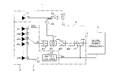
This radar apparatus is provided with a
transmitter section 1, an array antenna 2, a changeover
switch section 3, a receiving circuit section 4, and a
digital signal processing section 5. The array antenna
2, the changeover switch section 3, and the receiving
circuit section 4 compose a receiver section.
The transmitter section 1 is composed of a
voltage-controlled oscillator 11 having the center
frequency of f0 (for example, 76 GHz), a buffer
amplifier 12, a transmission antenna 13, and an RF
amplifier 14. The oscillator 11 outputs the modulated
CA 02330430 2000-10-27
TYT 98 -18
wave (transmitted signal) of f0 ~ OF/2, based on a
control voltage outputted from a do power supply for
modulation not illustrated. The modulated wave is
amplified by the buffer amplifier 12 and is radiated as
an electromagnetic wave from the transmission antenna
13. Part of the transmitted signal is amplified by the
RF amplifier 14 to be supplied as.a local signal for
downconversion.
The array antenna 2 for reception has nine
antenna elements corresponding to respective channels
from the first channel (CH1) to the ninth channel (CH9).
The changeover switch section 3 is comprised of a
switch body 31 and a switch control 32. The switch
body 31 has nine input terminals and one output
terminal and each antenna element of the array antenna
2 is connected to a corresponding input terminal. The
output terminal is designed to be connected to either
one of the input terminals and the connection thereof
is changed over properly in response to a changeover
signal from the switch control 32. The changeover of
connection is carried out electrically on the circuitry
and the sequence of changeover will be described
hereinafter.
The receiving circuit section 4 is composed of an
RF amplifier 41, a mixer 42, an amplifier 43, a filter
44, and an A/D converter 45. The RF amplifier 41
11
CA 02330430 2000-10-27
TYT 98 -1 ~
amplifies a signal outputted from the output terminal
of the switch body 31, which is a signal received by
either antenna element of the array antenna 2, and the
mixer 42 mixes the amplified signal with part of the
transmitted signal from the RF amplifier 14. The
received signal is downconverted by this mixing to
generate a beat signal as a difference signal between
the transmitted signal and the received signal. The
beat signal is supplied via the amplifier 43 and the
low-pass filter 44 to the A/D converter 45 to be
converted into a digital signal at the timing of a
signal from the switch control 32, i.e., at the timing
of a clock signal fsw for execution of connection
changeover in the switch body 31.
The digital signal processing section 5 executes
the digital beamforming (DBF) operation with digital
beat signals from the A/D converter 45 to detect the
target from the result thereof.
Described next is the operation of the FM-CW
radar apparatus constructed as described above.
Fig. 4 is a flowchart to show the operation of
the FM-CW radar apparatus and Fig. 5 is a timing chart
to show the changeover timing sequence of the
changeover switch section 3.
In the flowchart of Fig. 4, i indicates a channel
number of each antenna element, j a sampling number of
12
CA 02330430 2000-10-27
TYT 98 -13
a received wave in each of an up interval and a down
interval of triangular modulation, and k a period
number of triangular modulation. In the present
embodiment, i takes values of 1 to 9, j values of 1 to
N (for example, 128), and k values of 1 to 4.
First, in step S41 i, j, and k are set to "1" of
their respective initial value. It is then determined
in step S42 whether a signal is in a reading-in zone of
a sampling clock signal. In the present embodiment a
reading-in zone is a central section of each of the up
interval and down interval of the triangular modulation.
The reason is that higher linearity can be assured in
the central part of each interval than near a change
point from an up interval to a down interval or from a
down interval to an up interval of the triangular
modulation.
If the signal is in a clock signal reading-in
zone the flow will proceed through step S43 to S44 and
then to step S45 at a time of detecting an edge of a
clock signal to effect changeover of the switch body 31.
Since i = 1 at present, this changeover causes the
first antenna element chl to be connected to the switch
body 31.
With this changeover of the switch, a signal
received by the first antenna element chl is
downconverted in the mixer 42 and a beat signal thereof
13
CA 02330430 2000-10-27
TYT 9~ -18
is sent to the A/D converter 45.
Next, step S46 is to give a delay of half of a
clock period (1/fsw) and step S47 thereafter is to
carry out the A/D conversion of the beat signal by the
A/D converter 45 to read its digital beat signal into a
buffer of the digital signal processing section 5. The
delay in step S46 is given for carrying out the A/D
conversion operation at a center point of one antenna
element connection period, which permits the A/D
conversion to be executed during a stable period of
connection. The reading operation of the digital beat
signal into the buffer is carried out for each of i, j,
and k and for each of up and down intervals, for the
subsequent process.
After completion of this operation of one A/D
conversion, the flow moves to step 548. The operation
from step S48 to step S57 described below is a flow of
determining the sequence of the antenna elements to be
connected to the receiving circuit section 4 by the
changeover switch section 3. In this embodiment
selection of all the antenna element channels is
completed using four repetition periods of the
frequency modulation.
Fig. 5 is a timing chart to show an order of
selection of the antenna element channels, in which the
time is on the horizontal axis. In Fig. 5, CH.1 to
1=~
CA 02330430 2000-10-27
TYT 9~ -1~
CH.9 indicate the connection timing of the first to
ninth antenna element channels, in which high levels
represent connection. A waveform 51 represents the
timing of triangular modulation. For easy
understanding of illustration, the connection time
(high level period) of each channel is illustrated as
much longer than the actual connection time in the
relation to the waveform 51.
As seen from this figure, the first, second, and
third antenna elements are selected in the first
periodic interval and these are connected repeatedly in
order. In the second periodic interval the first, the
fourth, and fifth antenna elements are selected and
these are connected repeatedly in order. In the third
periodic interval the first, sixth, and seventh antenna
elements are selected and these are connected
repeatedly in order. In the fourth periodic interval
' the first, eighth, and ninth antenna elements are
selected and these are connected repeatedly in order.
The first antenna element is always selected as a
reference antenna element in the first to the fourth
periodic intervals, and the second to ninth antenna
elements are assigned two each to the first to the
fourth periodic intervals. A beat signal based on a
signal received by the first antenna element is
utilized as a reference signal for phase correction in
CA 02330430 2000-10-27
TYT 9S -1s
the DBF synthesis described hereinafter.
The operation from step S48 to step S57 for
carrying out such changeover connection of the antenna
elements is as follows.
Step S48 is to determine whether i = 1. If i = 1
then the flow goes to step S49 to replace i with (i +
(2k - 1)). Unless i = 1 the flow.goes to step S50 to
replace i with (i + 1). After that, step SS1 is to
determine whether i is greater than (2 + (2k - 1)).
Since i = k = 1 at present, the flow moves to
step S49 to set i = 2 and then returns via the
determination in step S51 to step 542. Then a digital
beat signal of a signal received by the second antenna
element is read into the buffer through steps S42 to
547. Since i = 2 at this point, the flow moves from
step S48 to step S50 to set i = 3 and again returns
from step S51 to step 542. Then a digital beat signal
of a signal received by the third antenna element is
read into the buffer through steps S42 to 547.
?Q Subsequent to it, the flow transfers from step
S48 to step S50 to set.i = 4. Then step S51 results in
making a positive judgment. Then the flow transfers to
step S52 to set i = 1 and also set j - 2.
After that, the flow transfers to step S53 to
2~ compare j with N. The value N is the number of
samplings in each antenna element channel in an up
1G
CA 02330430 2000-10-27
TYT 9~ -1~
interval and in a down interval, and in this embodiment
N = 128, for example. Since j - 2 at present, the flow
returns to step S42 with i = 1 and j - 2. After that,
digital beat signals of the first to the third antenna
elements are read in successively before j becomes 3 in
step S52.
Thereafter, digital beat signals of the first to
the third antenna element channels are successively
taken in similarly. After N digital beat signals have
been taken in every channel, the flow moves to step 554,
based on the determination in step 553, to return the
value of j to "1" of its initial value.
Next step S55 is to determine whether the digital
beat signal reading-in operation executed above is one
in an up interval or in a down interval. Since the
present status is just after completion of the reading-
in in the up interval, the determination in step S55 is
negative and thus the flow returns to step 542.
Thereafter, digital beat signals of the first to the
third antenna element channels are read in by 128
samples per channel in the down interval of the first
periodic interval.
After completion of the digital beat signal
reading-in operation in the down interval of the first
periodic interval, the flow transfers from step S55 to
step S56 to replace k with (k + 1). Since k = 1 at
17
CA 02330430 2000-10-27
TYT 98 -18
present, k = 2 is set here and then the flow returns
via the determination in step S57 to step S42.
By repeating the operation from step S42 to step
S55 thereafter, the first, the fourth, and the fifth
antenna elements are successively selected in each of
the up interval and the down interval of the second
periodic interval, as illustrated. in Fig. 5, whereby
the digital beat signals thereof are read in repeatedly.
When in step S56 k is set to 3, the first, the
sixth, and the seventh antenna elements are
successively selected in each of the up interval and
down interval of the third periodic interval, as
illustrated in Fig. 5, whereby the digital beat signals
thereof are read in repeatedly. Further, when k = 4,
the first, the eighth,, and the ninth antenna elements
are successively selected in each of the up interval
and down interval of the fourth periodic interval,
whereby the digital beat signals thereof are read in
repeatedly.
After completion of the above processing, all the
digital beat signals of the signals received by all the
antenna element channels have been read in the buffer
of the digital signal processing section 5. At this
time, the value of k is set as k = 5 in step S56 and
step S57 results in the positive. Thus the flow goes
to step S58.
18
CA 02330430 2000-10-27
TYT 98 -l~
Step S58 is to execute complex FFT operation of
each channel, DBF synthesis, and recognition operation
of target object based on the result thereof. After
step 558, the flow returns to step S41 to execute the
processing described above, and this is repeated
thereafter.
Next, the procedures of the;DBF synthesis in the
digital signal processing section 5 will be described
referring to the flowchart of Fig. 6.
Step S60 is to carry out the complex FFT
operation, as a pretreatment for the DBF synthesis, for
the digital beat signals in each channel and step S61
is to read in this FFT data of each channel. This FFT
operation yields frequency peaks according to the
target in every channel. Since it is sufficient that
the DBF synthesis is carried out selectively for the
frequency peaks, step S62 is a step of extracting
frequency points for the DBF synthesis.
Next, with the frequency points extracted in step
562, the operation from step S63 to step S67 is carried
out to convert and correct the phase and amplitude in
each channel. Step S63 is to determine whether data is
of the first periodic interval out of the first to the
fourth periodic intervals of the frequency modulation.
If the interval is either of the second periodic
interval to the fourth periodic interval, the flow goes
19
CA 02330430 2000-10-27
TYT 9s -Is
to step S65 to carry out phase compensation between
intervals based on the reference of the first antenna
element channel.
It is conceivable that between different periodic
intervals of the frequency modulation for reading-in of
digital beat signals there is change in the distance to
the target during the time difference, and the received
signals thus have a phase difference in each periodic
interval.
In this embodiment, therefore, the first antenna
element is used as a reference antenna element, the
digital beat signals of the signals received by the
first antenna element are read in all the periodic
intervals, and phases of the digital beat signals based
on the received signals by the other antenna elements
are corrected using the phase difference between the
intervals. The phases stated herein means those of the
original signals and those phases are also reserved in
the beat signals after downconversion. Thus the phase
differences can be detected.
Since in the second periodic interval the digital
beat signals based on the received signals by the first,
the fourth, and the fifth antenna elements are read in,
the phase difference is obtained between the phase
gained from the digital beat signal of the first
antenna element therein and the phase gained from the
CA 02330430 2000-10-27
TYT 9~ -18
digital beat signal of the first antenna element in the
first periodic interval. Then the phases of the
received signals by the fourth and fifth antenna
elements are reversed by the degree of the phase
difference, whereby they may be handled as signals on
an equal basis to those read in the first periodic
interval.
By executing the like correction in the third and
fourth periodic intervals, the received signals by all
the antenna elements may be handled as signals read in
the first periodic interval.
Step S64 is to carry out initial phase correction,
initial amplitude correction, and amplitude
distribution control specific to the apparatus, which
is commonly carried out in the DBF synthesis, in each
channel.
Next, step S66 is to execute phase rotation based
on a directional angle selected at present, and vector
composition between channels. Compensation for the
phase delay by the changeover switch is also carried
out herein.
After completion of the vector composition for
all the antenna element channels, the flow moves to
step S68 to extract information about peak frequencies
resulting from the composition.
It is determined in step S69 whether this
21
CA 02330430 2000-10-27
TYT 93 -1~
extraction of information about the peak frequencies is
finished for all the frequencies extracted in step 562,
as those to be subjected to the DBF synthesis. After
completion of the extraction ofninformation for all the
frequencies to be subjected to the DBF synthesis, the
flow transfers to step S70 to shift the directional
angle by 0.5° and then the operation from step S63 to
step S69 is executed again. This operation is repeated
forty one times at intervals of 0.5° from -10° to +10°,
whereby the scan based on the DBF synthesis is achieved
in the resolution of 0.5°.
The FFT operation and DBF synthesis illustrated
in Fig. 6 are carried out in each of the up interval
data and down interval data. After that, pairing is
carried out between frequency peaks in the up interval
and in the down interval to obtain information about
the velocity, distance, and direction of the target
object, based on the result thereof.
Next, another embodiment of the present invention
will be described. Fig. 7 is a diagram to show the
structure of the FM-CW radar apparatus as a second
embodiment of the present invention. The FM-CW radar
apparatus of the first embodiment is designed to effect
the homodyne detection, whereas the radar apparatus of
the present embodiment is designed to decrease the
noise by carrying out the heterodyne detection.
22
CA 02330430 2000-10-27
TYT 9~ -1~
In Fig. 7, like elements are denoted by identical
reference symbols to those in Fig. 1, and the detailed
description thereof will be omitted herein. The
changeover switch section 6 is composed of a switch
body 61 and a switch control 62, similar to the
changeover switch section 3 of Fig. 1. The switch body
61 has nine input terminals and one output terminal,
and the output terminal is connected to either one of
the input terminals. The connection of the output
terminal is changed over at regular intervals according
to a changeover signal from the switch control 62. The
difference from the switch body 31 of the first
embodiment is that the connection between the input
terminals and the output terminal is interrupted by
intermittent signals supplied from the outside. The
switch control 62 is the same as that 32 of the first
embodiment.
The receiving circuit section 7 is constructed in
such structure that an IF amplifier 71 and a second
mixer 72 are interposed in series between the mixer 42
and the amplifier 43 of the receiving circuit section 4
of Fig. 1. Further, it has an oscillator 73 for
outputting the intermittent signals fIF having the
frequency equal to several ten times that of the
changeover signal fsw. An example of the frequencies
of the respective signals is as follows; the frequency
23
CA 02330430 2000-10-27
TYT 98 -l~
f0 of the transmitted signal is, for example, 76 GHz,
the frequency fIF of the intermittent signals in an
intermediate frequency band is, for example, 100 MHz,
the frequency of the changeover signal is, for example,
5 MHz, and the frequency of the beat signals is, for
example, DC to 100 kHz.
Fig. 8 is a spectral map to,show the way of
frequency conversion in the signal processing operation
in the present embodiment. In the FM-CW radar
apparatus of the present embodiment, a received signal
130 is replaced with signals 131 and 132 by on/off
according to the intermittent signals in the changeover
switch section 6 and thereafter they are downconverted
to an intermediate signal 133 in the mixer 42.
Subsequent to it, the intermediate signal 133 is
downconverted to a beat signal 134 in the second mixer
72.
In Fig. 8, a curve 136 indicates a noise floor of
the mixer 42 and a curve 136 a noise floor of the
second mixer 72. As seen from this figure, the mixer
42 downconverts the signals into the IF zone where the
influence of noise is low. Then the second mixer 72
having lower noise in the low frequency band than the
mixer 42 downconverts the signal to the beat signal.
Therefore, the present embodiment may expand the noise
margin considerably, as compared with the homodyne
CA 02330430 2000-10-27
TYT 93 -18
method.
Since the mixer 42 has the very wide bandwidth,
there normally appears a lot of 1/f noise and FM-AM
conversion noise by the FM-CW method in the low
frequency range. In contrast, since the second mixer
72 has the narrow bandwidth, the noise floor is lowered.
The present embodiment achieves the expansion of noise
margin by making use of such action.
If the IF amplifier 71 prior to the second mixer
72 has a narrower band, the IF signal may be separated
from the FM-AM conversion noise appearing in the low
frequency range, so that the low-frequency noise may be
decreased further.
In the first and second embodiments the number of
channels of the antenna elements was nine, but the
detection accuracy may be enhanced further by
increasing the number of channels.
Industrial Applicability
As described above, the FM-CW radar apparatus of
the present invention needs only one set of the
expensive devices. necessary for the downconversion, for
example, the RF amplifier, the high-frequency mixer,
etc., regardless of the number of antenna elements.
Therefore, the whole apparatus may be constructed at
low cost and in compact size.
CA 02330430 2000-10-27
TYT 9~ -l~
In addition, the switch means connects only part
of the antenna elements to the beat signal generating
circuit in one period of the repetition periods of
frequency modulation, so that the switching frequency
may be lower than in the case wherein all the antenna
elements are connected to the beat signal generating
circuit in one period. Further taking it into
consideration that a beat signal is sampled every
changeover of connection, the A/D conversion rate may
also be decreased with decrease in the switching
frequency. This permits use of cheaper switch element
and A/D converter.
26