Note : Les descriptions sont présentées dans la langue officielle dans laquelle elles ont été soumises.
CA 02330536 2000-10-27
WO 99/62085 PCT/US99/10079
POWER REGULATOR
Field of the Invention
This invention relates to a power regulator and a method of
regulating power. In particular, the invention relates to a power regulator in
which power regulation is achieved by either changing the frequency of an AC
source closer to or farther away from the resonance frequency of a tuned
circuit,
or where there is a fixed frequency AC source, by changing the resonance
frequency of a tuned circuit closer to or away from the frequency of the AC
source.
I0 Background of the Invention
Several methods are known for regulating the output power of a
power supply. In switched mode power supplies, regulation by means of pulse
width modulation is the most common method used. Another method of
regulating output power is the use of a tuned circuit in series with an AC
voltage
source. The tuned circuit includes an inductance and a capacitor and has a
resonance frequency associated with it. FIG. 1 shows the attenuation curve of
a
series connection of an inductance L and a capacitance C acting as an LC
filter as
a function of frequency. The resonance frequency Fres of the inductance L and
the capacitance C is given by Equation 1 for the simplest circuit that can be
used
for power regulation to a resistance load employing a resonant circuit (an LC
filter)
Fres =1 / (2~ LC ~ (Eq. l)
By definition, the attenuation at the frequency Fres is 1, meaning that all
energy
passes through the circuit and there is maximum power. In the regions adjacent
the resonance frequency Fres, only a portion of the energy passes through.
Power output to a load resistance from an LC filter may be
regulated by adjusting the correspondence between the frequency of an AC
source
CA 02330536 2000-10-27
WO 99/62085 PCT/US99/100'79
-2-
Power output to a load resistance from an LC filter may be
regulated by adjusting the correspondence between the frequency of an AC
source
and the frequency of the resonant circuit formed of the LC filter with
inductance
L and capacitance C. The correspondence between the frequency of an AC source
and the frequency of a resonant circuit may be adjusted by either changing the
frequency of the AC source closer to or farther away from the resonance
frequency of the resonant circuit, or, in the case of a fixed frequency AC
source,
by changing the resonance frequency of the resonant circuit closer to or away
from the frequency of the AC source. FIG. 2 illustrates attenuation curves for
power regulation accomplished by changing the resonance frequency of a
resonant circuit closer to or farther away from the AC source. More
particularly,
in FIG. 2, Fac is the frequency of the AC source signal. Fres.l is the
attenuation
curve of an LC filter, as in FIG. 1. The point A where the frequency of the AC
source Fac crosses the attenuation curve for the LC filter having a resonance
frequency Fres.l, illustrates the amount of attenuation of the frequency of
the AC
source Fac that is achieved by the LC filter. In the situation illustrated,
the
amplitude of the signal after the LC filter is reduced by the LC filter to
about 15%
of the amplitude of the frequency of the AC source Fac as shown by point A.
However, if the curve of the resonance frequency is moved in the
direction of the frequency of the AC source Fac, the attenuation of the
frequency
of the AC source Fac by the LC filter changes, and the voltage output
amplitude
rises, increasing the power output. The curve of the resonance frequency may
be
moved in the direction of the frequency of the AC source Fac by changing one
or
both of the values of the inductance L and the capacitance C in accordance
with
Equation 1 above. In FIG. 2, this shift is illustrated by moving the curve of
the
resonance frequency Fres.l in the direction of the horizontal arrow to a new
resonance frequency Fres.2. The point B where the frequency of the AC source
Fac crosses the new attenuation curve shows that the signal after the LC
filter is
CA 02330536 2000-10-27
WO 99/62085 PCT/US99/10079
-3-
increased to about 90% of the amplitude of the frequency of the AC source
signal
Fac as shown by the vertical arrow. Thus, the output voltage and hence the
output power are increased. By changing the resonance frequency of the
inductance L and the capacitance C of the resonant circuit, the output power
delivered by the power supply to a load resistance can be regulated.
A second method of power regulation is achieved by changing the
frequency of an AC source closer to or farther away from the resonance
frequence
of a resonant circuit. FIG. 3 illustrates this method graphically where the
resonance frequency Fres is kept constant, while the graph of frequency of the
AC
source is varied from Facl to Fac2 in the direction of the horizontal arrow.
For
the first frequency of the AC source Facl, the point of crossing of the
attenuation
curve and Facl results in an amplitude after the LC filter of about 15% of the
amplitude of the frequency of the AC source Fac. When the frequency of the AC
source is decreased as indicated by the horizontal arrow to the value Fac2,
the
attenuation of the frequency of the AC source by the LC filter changes and the
output amplitude rises. At the new frequency of the AC source Fac2, the point
B
of crossing of the attenuation curve increases to about 90% of the amplitude
of
the frequency of the AC source as shown by the vertical arrow. Accordingly,
the
output voltage and the output power to a load resistance is increased. By
changing the frequency of the AC source from Facl to Fac2, power can be
regulated.
FIG. 4 shows a prior art power regulator for supplying power to a
resistance load which performs power regulation by a resonant circuit which is
more complicated than just the LC filter discussed above. More particularly,
the
power regulator 10 illustrated in FIG. 4 has an AC source 11, a resonant
circuit
12, an isolation transformer 13, rectifying means 14, and an output across
terminals 18 and 19 for connecting to the load resistor R,oed 20. The resonant
circuit 12 includes an inductance L and a capacitance C. The rectifier means
14
CA 02330536 2000-10-27
WO 99/62085 PCTIUS99/100'79
-4-
is a rectifier and includes a diode circuit made up of diodes I5 and 16, and a
smoothing capacitor 17. A circuit in accordance with prior art FIG. 4 is
disclosed
in U.S. Patent No. 4,930,063, issued to Henze et al. on May 29, 1990, and
includes a variable inductor for the inductance L of the resonant circuit.
Accordingly, in the Henze et al. regulator for a power supply, the resonance
frequency is varied by varying the inductance of the resonant circuit in order
to
regulate power. An attenuation curve similar to that of FIG. 1 may be obtained
for the prior art circuit in the Henze et al. Patent, and power regulation may
be
obtained by changing the resonance frequency of the resonant circuit in a
manner
similar to that graphically illustrated in FIG. 2.
Several disadvantages are associated with the prior art circuits for
power regulation employing resonant circuits. As illustrated in the
attenuation
curves of FIGS. 1-3, the attenuation curve for each circuit approaches but
never
equals zero amplitude of the frequency of the AC source. The output power can
never equal zero. This is because the attenuation of the LC filters of the
prior art
circuits would have to be substantially infinitely high in order to regulate
to a
voltage lower than the AC source voltage when the current at the output of a
circuit is equal to essentially zero and the resistance of the load connected
to the
circuit is substantially infinite. A minimum power output can only occur at
substantially an infinitely high source frequency or at substantially an
infinitely
large inductance L. Further, the diodes in the rectifier result in significant
recovery losses due to significant instantaneous reverse voltages immediately
after
recovery. In prior art circuits, the voltages across the diodes of the
rectifier are
subject to sharp transitions. Further, the prior art circuits are subject to
parasitic
effects from the leakage inductance of the isolation transformer, the winding
capacitances of the isolation transformer, and capacitances associated with
the
diodes of the rectifier. Further, isolation transformers are associated with
power
CA 02330536 2000-10-27
WO 99/62085 PCT/US99/10079
-5-
dissipation due to the resistance of the copper windings referred to as copper
losses of the windings.
There is therefore a need for a power regulator that regulates power
by adjusting the correspondence between the frequency of an AC source and the
resonance frequency of a resonant circuit which permits power regulation
between a maximum value and a minimum value of zero. Further, there is a need
for a power regulator employing a resonant circuit that reduces the recovery
loss
in diodes employed in the rectifier. Additionally, there is a need for a power
regulator that regulates power by employing a resonant circuit that reduces or
eliminates the parasitic effects due to transformer leakage, copper losses of
transformer windings, unwanted winding capacitances associated with a
transformer, and unwanted capacitances associated with diodes in the rectifier
means.
Summary of the Invention
It is an object of the invention to provide a power regulator which
regulates output power employing a series resonant circuit which can regulate
power between a maximum value and a minimum value of zero or essentially
zero.
A further object of the invention is to provide a power regulator
which regulates power employing a series resonant circuit that reduces the
recovery loss associated with diodes in the rectifier.
It is a further object of the invention to provide a power regulator
which regulates power employing a series resonant circuit that reduces the
parasitic effects of leakage inductance of a transformer of the power
regulator.
It is still a further object of the invention to provide a power
regulator which regulates power employing a series resonant circuit that
reduces
the parasitic effects of winding capacitances of a transformer of the power
regulator.
CA 02330536 2000-10-27
WO 99/62085 PCT/US99/10079
-6-
Additionally, it is an object of the invention to provide a power
regulator that regulates power employing a series resonant circuit that
reduces
the parasitic effects of capacitances associated with diodes of the rectifier
of the
power regulator.
It is still another object of the invention to provide a power
regulator which regulates power employing a series resonant circuit that
reduces
copper losses associated with the windings of a transformer of the power
regulator.
These and other objects of the invention are accomplished by
providing a power regulator comprising: an AC source having a voltage and a
frequency; ari output having an output voltage Vo"~; a first resonant circuit
comprising a first inductance Ll and a first capacitance C1 connected in
series to
the AC source, and having a first resonance frequency; means for adjusting the
correspondence between the frequency of the AC source and the first resonance
frequency of the first resonant circuit in order to regulate power; and means
for
regulating to an output voltage lower than the voltage of the AC source when
there is essentially zero output current.
In a preferred embodiment of the power regulator the means for
regulating comprises a second capacitance C2 connected in parallel with the
output to form a second resonant circuit with the first inductance Ll.
These objects are further accomplished by providing a power
regulator comprising: an AC source having a voltage and a frequency; an output
having an output voltage Vo"~; a first resonant circuit comprising a first
inductance
Ll and a first capacitance Cl connected in series to the AC source, and having
a
first resonance frequency; means for adjusting the correspondence between the
frequency of the AC source and the first resonance frequency of the first
resonant
circuit in order to regulate power; and a second capacitance C2 connected in
CA 02330536 2000-10-27
WO 99/62085 PCT/US99/10079
_7_
parallel with the output to form a second resonant circuit with the first
inductance Ll.
Also disclosed is a method of regulating power comprising:
adjusting the correspondence between a frequency of an AC source and a
resonance frequency of a first resonant circuit comprising a first inductance
Ll
and a first capacitance C1 connected in series to the AC source to regulate
power
at an output; and regulating the output voltage of the power regulator to a
value
lower than the voltage of the AC source when there is essentially zero current
at
the output.
The above and other objects, aspects, features and advantages of the
invention will be more readily apparent from the description of the preferred
embodiments thereof taken in conjunction with the accompanying drawings and
appended claims.
Brief Description of the Drawings
The invention is illustrated by way of example and not limitation
in the figures of the accompanying drawings in which like references denote
like
or corresponding parts, and in which:
FIG. 1 illustrates an attenuation curve for an LC filter according to
the prior art;
FIG. 2 illustrates the change in attenuation curves when the
resonance frequency is adjusted to regulate power in accordance with the prior
art;
FIG. 3 illustrates the change in crossing points of the attenuation
curve when an AC source frequency is varied to regulate power in accordance
with the prior art;
FIG. 4 is a power regulator in accordance with the prior art;
FIG. 5 is a power regulator in accordance with a first embodiment
of the invention;
CA 02330536 2000-10-27
WO 99/62085 PCT/US99/10079
_g_
FIG. 6 is a power regulator in accordance with a second
embodiment of the invention;
FIG. 7 is a power regulator in accordance with a third embodiment
of the invention;
FIG. 8 is a power regulator in accordance with a fourth embodiment
of the invention;
FIG. 9 is a power regulator in accordance with a fifth embodiment
of the invention;
FIG.10 is a power regulator in accordance with a sixth embodiment
of the invention;
FIG.11A shows waveforms for the signals identified for a preferred
embodiment of the power regulator of the invention in accordance with FIG.10,
employing an AC voltage source with a square wave;
FIG.11B shows waveforms for the signals identified for a preferred
embodiment of the power regulator of the invention in accordance with FIG.10,
employing an AC voltage source with a sine wave;
FIG. 12 shows the waveforms of IdI and the voltage across the
diode D1 for the embodiments of the invention illustrated in FIGS. 7-10;
FIG. 13 shows the waveforms of Idl and Id2 for the embodiments
of the invention illustrated in FIGS. 7-10 above emphasizing the slow rate of
change in the current of the diodes D1 and D2;
FIG.14 shows the waveforms of the source voltage and the voltage
at Val when Ll is increased and the load resistance is at infinity;
FIG. 15 shows the waveforms of Iin and Val where C2 is equal to
C2n,;";
FIG. 16 shows the waveforms of Iin and Val where C2 is smaller
than C2m;n;
CA 02330536 2000-10-27
WO 99/62085 PCT/US99110079
_g_
FIG. 17 shows the waveforms for Iin and Va1 where C2 is larger
than C2m;"; and
FIG. 18 shows the waveforms for Iin and Val where C2 is much
larger than C2m;n in accordance with the waveforms illustrated in FIGS. 11A
and
11B.
Description of the Preferred Embodiments
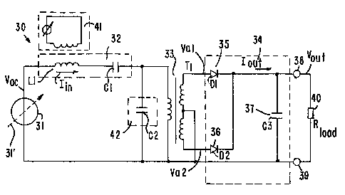
Refernng to FIG. S a power regulator 30 in accordance with a first
embodiment of the invention supplies power to a resistance load Road 40 and
performs power regulation by a series resonant circuit 32. More particularly,
the
power regulator 30 illustrated in FIG. 5 has a source of voltage which is an
AC
source 31 of a sine wave or a square wave. The shape of the AC source waveform
is not important to the voltages and currents that are obtained by the
regulator.
The resonant series circuit 32 includes inductance Ll and capacitance CI. The
circuit further includes an isolation transformer 33 and rectifier means 34
for
providing a DC output at terminals 38 and 39 of the power regulator. The
resistance load 40 is connected across the output at terminals 38 and 39. The
rectifier means 34 is a rectifier which includes a diode circuit made up of
diodes
35 and 36 (Dl and D2), and a smoothing capacitor 37 (C3). The voltage source
31 has a voltage Vac and a frequency Fac. The output across terminals 38 and
39 has an output voltage Vo"~. The resonant circuit 32 includes the inductance
Ll
and the capacitance Cl connected in series to the AC source and has a
resonance
frequency Fres.
CA 02330536 2000-10-27
WO 99/62085 PCT/US99/10079
-10-
In the embodiment illustrated in FIG. 5, the resonance frequency of
the resonant circuit 32 may be changed by changing the inductance Ll wtuch is
illustrated in the figure as a variable inductance. Alternatively, the
capacitance
Cl may be variable in order to change the resonance frequency of the resonant
S circuit 32. Further, both the inductance Ll and the capacitance C1 may be
changed to change the resonance frequency of the resonant circuit 32. Changing
the resonance frequency of the resonant circuit 32 is one manner of adjusting
the
correspondence between the frequency of the AC source 31 and the resonance
frequency Fres of the resonant circuit 32 in order to regulate the power of
the
power regulator 30. Thus, the illustrated means 41 for adjusting the
inductance
Ll of the resonant circuit may be considered a means for adjusting the
correspondence between the frequency of the AC source 31 and the resonance
frequency Fres of the resonant circuit 32. Additionally, any known means for
varying the capacitance Cl may be considered a means for adjusting the
correspondence between the frequency of the AC source 31 and the resonance
frequency Fres of the resonant circuit 32 in order to regulate power.
Alternatively, the correspondence between the frequency of the AC source and
the
resonance frequency of the resonant circuit 32 may be adjusted employing a
variable AC source, illustrated in FIG. S by the dashed arrow 31'.
Accordingly, the
circuitry within the variable AC source 31' that varies the signal frequency
may
be considered a means for adjusting the correspondence between the frequency
CA 02330536 2000-10-27
WO 99/62085 PCT/US99/10079
-11-
of the AC source and the resonance frequency Fres of the resonant circuit 32.
In
another alternative, the correspondence between the frequency of the AC source
31 and the resonance frequency Fres of the resonant circuit 32 may be adjusted
employing a variable AC source frequency and/or any known means for varying
the inductance Ll and the capacitance Cl combined.
The first embodiment illustrated in FIG. 5 further includes the
capacitor C2, which is connected in parallel with the output across output
terminals 38 and 39 and forms a second resonant circuit with the inductance Ll
of the first resonant circuit 32. The capacitance C2 is connected on the
primary
side of the isolation transformer 33 and permits regulating to an output
voltage
lower than the voltage of the AC source when there is essentially zero output
current. Accordingly, the capacitance C2 permits the power regulator 30 to
obtain an output power of essentially zero.
The transformer 33 has a primary winding and at least one
secondary winding with a center tab that is connected to the output terminal
39.
The outputs of each end of the secondary winding are rectified by a diode
circuit
of rectifier means 34 including diodes 35 and 36 to deliver a DC output
current
Iout and output voltage Vo"~. The rectifier means 34 further includes a
smoothing
capacitor 37 (C3). The transformer 33 has associated therewith a leakage
inductance Tl.
CA 02330536 2000-10-27
WO 99/62085 PCT/US99/10079
-12-
In operation, the first embodiment of the invention includes a
resonant circuit 32 having an inductance Ll and a capacitance C1 connected in
series to an AC source. Power is regulated by adjusting the correspondence
between the frequency of the AC source Fac and a resonance frequency of the
resonant circuit Fres. Further, the output voltage is regulated to a value
lower
than the voltage of the AC source when there is substantially zero current at
the
output. A parallel capacitance C2 is added to regulate the output voltage to a
value that is lower than the voltage of the AC source when the output current
is
essentially zero. The capacitance C2 is connected across the primary winding
of
the transformer 33. The capacitance C2 forms a second resonant circuit with
the
inductance Ll of the resonant circuit 32. The use of a second resonant circuit
permits the second resonant circuit to act as low-pass filter when the output
current is essentially zero.
The impedance of the primary winding of the transformer 33 at the
frequency of the AC source is many times higher than the impedances of
inductance Ll, capacitance Cl and capacitance C2. Accordingly, the impedance
of the primary inductance is high enough to have a negligible influence on the
resonance frequencies of the resonant circuit Ll and Cl and the resonant
circuit
L1 and C2. The values of the source frequency and the resonance frequency of
the resonant circuit comprising Ll and Cl are set so that the resonance
frequency
Fres is placed just under the source frequency Fac, and the power is regulated
by
CA 02330536 2000-10-27
WO 99/62085 PCT/US99/10079
-13-
changing either the resonance frequency of the resonant circuit 32 or by
changing
the source frequency employing an optional variable AC source 31'. The
operation is the same if the AC source frequency is placed below the resonance
frequency of Ll and C1, however, power regulation is achieved on the positive
slope of the LC filter.
The primary inductance of the transformer 33 is considered to be
infinitely large in the equation for the resonance frequency of the circuit
similar
to Equation 1 above. Accordingly, the primary inductance of the transformer 33
is so large that the resonance with any capacitor in the circuit is at least a
factor
20 of ten below the resonance of the resonant circuit 32. Accordingly, the
resonances of the primary winding of the transformer 33 with any of the
capacitances in the circuit may be considered negligible. The presence of C2
permits the second resonant circuit, including inductance Ll and capacitance
C2,
to have a low-pass filter effect which can give sufficient attenuation at a
finite and
practical value for the source frequency and for the value of the inductance
Ll.
The circuit uses only the fundamental frequency of the voltage
source. Accordingly, the AC signal from the voltage source is not limited to
any
specific waveform and may be a sine wave or a square wave. Reference may be
made to the corresponding waveforms shown in FIGS. 11A and 11B for the
embodiment with the specific values given for the circuit of FIG. 10.
CA 02330536 2000-10-27
WO 99/62085 PCT/US99/10079
-14-
To obtain minimum output power, the frequency of the AC source
is caused to be the farthest away from the resonance frequency Fres of the
resonant circuit 32. Assuming the case of a fixed frequency AC source, the
value
of inductance Ll is chosen high for a low resonance frequency of the resonant
circuit formed by Ll and C1 so that the attenuation curve is far below the AC
source frequency Fac. The large value of Ll also causes the resonance
frequency
of the resonant circuit formed by Ll and C2 to be below the frequency of the
AC
source Fac. The inductance Ll and the capacitance C2 form a low pass filter
for
the AC source frequency Fac. The values of the capacitors C1 and C2 are chosen
in such a way that the positive peak voltages Val and Va2 at the anodes of the
diodes D1 and D2 (34 and 35) are equal to or lower than the desired output
voltage Vo"~ in order for the minimum output power to equal zero. More
particularly, in order to achieve a zero power output at a given output
voltage
Vo"~, the peak voltage value Val at the anode of diode D1 must be equal to the
output voltage Vo"~.
The criterion to reach a zero or essentially zero output power for a
given output voltage Vout is that the attenuation of the fundamental frequency
of
the AC source Fac caused by the low pass filter formed of inductance Ll and
capacitance C2 is equal to the ratio of the peak amplitude of the fundamental
frequency of the AC source and the output voltage Vo"t. The operation of the
CA 02330536 2000-10-27
WO 99/62085 PCT/US99/10079
-15-
circuits is similar when the AC source frequency Fac is changed. The same
waveforms for current and voltage are obtained.
FIG. 6 is a second embodiment of the power regulator of the
invention. The second capacitance C2 is placed at the secondary side of the
transformer 33. More particularly, the capacitance C2 is connected across the
secondary winding of transformer 33 with a terminal of the capacitance C2
connected to each of the anodes of the diodes D1 and D2. The leakage
inductance Tl of the transformer 33 becomes part of the tuning circuit made up
of the inductor Ll, capacitor C1, the leakage inductance of the transformer Tl
and the capacitance C2. The sum of the leakage inductance Tl of transformer 33
and the inductance of inductance Ll constitute the inductive part of the
resonant
circuits. Accordingly, the value of the inductance Ll may be set to compensate
for the leakage inductance Tl of the transformer 33. Accordingly, the second
embodiment of the invention reduces the influence of the leakage inductance T1
of the transformer 33.
Placing the capacitance C2 across the secondary side of the
transformer 33 further permits the value of the capacitance C2 to be set to
compensate for the winding capacitances of the isolation transformer. Further,
the value of the capacitance C2 may be set to compensate for the capacitances
associated with the diodes D1 and D2 of the rectifier means 34. The parasitic
winding capacitances of the transformer 33 are fully across the capacitance C2
CA 02330536 2000-10-27
WO 99/62085 PCT/US99/100'79
-16-
and therefore form a part of the value of the capacitance C2. Further, the
junction capacitances of the diodes D1 and D2 are fully across the capacitance
C2
and therefore are a part of the value of the capacitance C2 as well.
FIG. 7 is a third embodiment of the power regulator according to
the invention. The third embodiment of the invention is similar to the first
embodiment of the invention illustrated in FIG. S, however, a series
inductance
L2 is added between the point of connection of the cathodes of the diodes D1
and
D2 and the output terminal 38. Like references on FIG. 7 denote like or
corresponding parts as in previous figures. However, in FIG. 7 the inductance
L2
is added to the rectifier means 34. Just as in the first embodiment shown in
FIG.
5, the turning circuit is limited to the inductor Ll and the capacitances C1
and
C2. The primary inductance of the transformer 33 and the inductance L2 are
chosen to be high enough to have a minimum influence on the resonant circuits.
More particularly, if the inductance L2 is set to a value that is so high that
the
waveform of the voltage of the signal delivered from diode D2 has little
influence
on the output current Iout through the inductance L2, the inductance LZ will
hardly influence the resonance frequencies of the resonant circuits formed of
inductance Ll, and capacitances C1 and C2.
FIG. 8 is a power regulator according to a fourth embodiment of the
invention. The power regulator illustrated in FIG. 8 is similar to that
illustrated
in FIG. 6 which places the capacitance C2 on the secondary side of the
isolation
CA 02330536 2000-10-27
WO 99/62085 PCT/US99/10079
-17-
transformer 33, however, the inductance L2 is added to the rectifier means 34
as
in the embodiment illustrated in FIG. 7. The series inductance L2 reduces the
recovery losses of the diodes D1 and D2 in the rectifier means 34. The
inductance
L2 serves the function of creating a high impedance for the AC voltage at the
cathodes of the diodes Dl and D2 and a low impedance for the DC output.
In order to reduce the reverse recovery losses in the diodes of the
rectifier, it is important that the diodes have as slow as possible a forward
current
transition and as slow as possible a reverse voltage transition. It is also
necessary
that each of the diodes only goes into reverse only once every period. FIGS.
12
and 13 show waveforms for the forward currents Idl and Id2 through the diodes
D1 and D2. FIG. 12 further shows the waveform for the voltage across the
diodes for diode D1. FIG. 12 shows the slow forward current increase and
decrease of D1 and the smooth increase of the reverse voltage across diode Dl.
The series inductance L2 causes the output current Iout to be a constant DC
value
(with a small AC-component) (see bottom waveforms of FIGS.11A and 11 B), and
current to be gradually taken over from one diode to the other. This is
highlighted by the circled portions of the waveforms of Idl and Id2 of FIG.
13.
After the current through the diode has reached zero, the reverse voltage
rises
smoothly as shown in the waveform of the voltage across diode D1 shown in FIG.
12. The slower the forward current in a diode is reduced, the smaller the
CA 02330536 2000-10-27
WO 99/62085 PCT/CTS99/10079
-18-
recovery charge is. Further, less of that recovery charge is dissipated in
heat, the
slower the reverse voltage rises. Accordingly, there are less recovery losses.
To achieve this mode of operation, a minimum value for C2 is
required. If C2 is too small, the diodes will go into reverse (out of
conduction)
more than once per period causing the reverse recovery loss to occur more than
once per period also. FIG. 16 shows the situation where C2 is 0.7 times the
minimum value C2m;". The diodes go out of conduction twice per period
resulting
in unacceptably high recovery losses.
The determination of the minimum value of C2 is as follows:
Diodes D1 and D2 will cause a double sided rectification of current
Iin, resulting in a DC output current Iout. If inductance L2 is assumed to be
infinitely large, then the output current Iout is equal to the average value
of the
input current Iin, being:
Iout = IinPk ((~ o -.(sin ~ )) / n) ~ Iout = approxØ64IinPk. (Eq. 2)
where Iin is assumed to be a perfect sine wave and ~ is the frequency of the
input.
If the momentary value of the input current Iin is below the output
current Iout, both diodes D1 and D2 conduct. This is illustrated by the
circled
areas of FIG. 13 illustrating the forward currents Idland Id2 through the
diodes
D1 and D2. If the momentary value of the input current Iin exceeds the output
current Iout, one of the diodes will go out of conduction and a 'half sine
wave
CA 02330536 2000-10-27
WO 99/62085 PCT/US99/10079
-19-
shaped'voltage waveform Val and Va2 occurs at the anodes of the diodes D1 and
D2. This voltage waveform is determined by the resonance of capacitance C2
with inductance L1.
The resonance of the resonant circuit C2 and Ll will only occur
when one of the diodes is not conducting, because when both diodes D1 and D2
are conducting, the capacitance C2 is short circuited by both of the
conducting
diodes, and hence the only resonance that then exists is due to inductance Ll
and
capacitance C1.
The exact formula for the resonance frequency of capacitance C2
is:
FresC2 = 1 / (2~c (L 1 (C 1 (4)C2 / (C 1 + 4C2)))) (Eq. 3)
The factor of 4 comes from the transformation ratio of the isolation
transformer
Tl.
Since capacitance C2 is much smaller than capacitance C1, this
equation can be simplified to:
FresC2 = 1 / (4~z (L 1 C2) (Eq. 4)
The criterion which must be met for setting the value of capacitance
C2 is that during the time that the momentary value (rather than the RMS
value)
of the input current Iin is larger than the output current Iout, there may not
be
more than one full cycle of the resonance frequency FresC2. If there would be
CA 02330536 2000-10-27
WO 99/62085 PCT/US99/10079
-20-
more than one cycle, the diodes would go out of conduction for more than once
every period resulting in excessive recovery losses.
Given Equation 1, the input current Iin will be higher than the
output current Iout when it reaches more than 0.64.IinPk, the average value of
the
input current. Consequently, during approx. 100 ° of the 360 °
period, the input
current Iin is higher than the output current Iout. This means that the
maximum
value of the resonance frequency FresC2 is 3.6 times the frequency of the
voltage
source Fac.
FresC2m~ _ (360 / 100)Fac (Eq. 5)
The minimum value for C2 is then:
C2m~ = 1 / ( 16p 2(3.6)2 Fac2L1) -~ C2",i~ = aPProx. 1/(204.7 Face
Ll ) (Eq. 6)
FIGS. 15, 16, 17 and 18 show waveforms for the input current Iin
and the voltage Val at the anode of diode Dl for different values of
capacitance
C2.
FIG. 15 shows the situation where capacitance C2 is equal to C2m;".
The waveform of the input current Iin shows clearly one full cycle of the
resonance frequency FresC2 in the peaks of the fundamental frequency.
FIG. 16 shows the situation where capacitance C2 is smaller than
C2m;n. More particularly, C2 = 0.7C2m;n. The waveform of the input current Iin
shows more than a full cycle of the resonant frequency FresC2 and the waveform
CA 02330536 2000-10-27
WO 99/62085 PCTNS99/10079
-21-
of the voltage Val shows two peaks in the place of one. The two peaks indicate
that the diode goes out of conduction twice per cycle resulting in twice the
recovery losses.
FIG. 17 shows the situation where capacitance C2 is larger than
C2m;n~ In FIG. 17 C2 = (3C2m;"). The waveform of Iin shows less than one full
cycle of the resonant frequency FresC2.
FIG. 18 shows the situation where capacitance C2 is much larger
than C2m;n. In FIG. 18 C2 = 6C2~,;". The waveform of the input current Iin is
close to a sine wave, because there is only about half a cycle of the
resonance
frequency FresC2 in the peaks of the input current Iin. The waveforms in FIGS.
11A and B were obtained setting the value of capacitance C2 much larger than
C2",in~
Since inductance Ll is variable when the frequency of the voltage
source Fac is constant, C2m;" has to be calculated for the minimum possible
value
of inductance Ll.
FIG. 9 shows a fifth embodiment of the invention which is similar
to that illustrated in FIG. 8 where like references denote corresponding
parts,
however, in FIG. 9 the transformer 33 is replaced with a transformer 44 having
a multitude of identical transformer windings 44a, 44b and 44c, wound
multifilar
and connected in series. The use of the identical windings in series on the
transformer and the multifilar winding method minimizes the leakage inductance
CA 02330536 2000-10-27
WO 99/62085 PCT/US99/10079
-22-
Tl of the transformer 44 and reduces the copper loss of the windings of the
transformer 44. In FIG. 9, the transformer 44 has three identical windings and
is used to obtain a transformation ratio from input to output of 2:1.
FIG. 10 is a power regulator in accordance with the sixth
embodiment of the invention where the transformer 45 has two identical
windings 45a and 45b wound multifilar and connected in series in order to
obtain
a transformation ratio from input to output of 1:1.
FIG.10 illustrating the sixth embodiment of the invention provides
the waveforms illustrated in FIGS.11A and 11B when the following values of the
components and voltages are employed.
Fac: 700kHz / 36Vpp square wave (or 42Vpp sine
wave)
Ll : 0.92~cH
Cl : 100nF
N1/N2: 1
C2: 4700pF
L2: 2.2~cH
C3: lOuF
Rload 1 ~
Vouc~ 12VDC
FIG. 11A illustrates the waveforms obtained employing an AC
voltage source with a square wave and FIG.11B shows the waveforms obtained
employing an AC voltage source with a sine wave. The actual waveform of the
AC source is insignificant as long as the fundamental frequency is at the
given
value for Fac. The shape of the waveform from the AC source has virtually no
impact on the voltages and currents obtained.
CA 02330536 2000-10-27
WO 99/62085 PCT/US99/10079
-23-
Also contemplated is a method of regulating power comprising:
adjusting the correspondence between a frequency of an AC source and a
resonance frequency of a first resonant circuit comprising a first inductance
Ll
and a first capacitance C1 connected in series to the AC source to regulate
power
at an output; and regulating the output voltage of the power regulator to a
value
lower than the voltage of the AC source when there is substantially zero
current
at the output. The step of regulating the output voltage lower than the
voltage
of the AC source when there is zero output current includes providing a second
capacitance C2 connected in parallel with the output to form a second resonant
circuit with the first inductance Ll.
Although the invention has been described with reference to the
preferred embodiments, it will be apparent to one skilled in the art that
variations
and modifications are contemplated within the spirit and scope of the
invention.
The drawings and description of the preferred embodiments are made by way of
example rather than to limit the scope of the invention, and it is intended to
cover
within the spirit and scope of the invention all such changes and
modifications.